AENSI Journals
Australian Journal of Basic and Applied Sciences
ISSN:1991-8178Journal home page: www.ajbasweb.com
Corresponding Author: Koh Wen Shi, Freescale Semiconductor (M) Sdn. Bhd., Free Industrial Zone Sungei Way, 47300 Petaling Jaya, Selangor, Malaysia.
Characterization of Laser Micromachining Process for Low-k / Ultra Low-k
Semiconductor Device
1,3Koh Wen Shi, 2Yap Boon Kar, 1Halina Misran, 3Yow Kai Yun, 3Lau Teck Beng and 3Lo Wai Yew
1Department of Mechanical Engineering, College of Engineering, Universiti Tenaga Nasional, KM-7, Jalan Ikram-Uniten, 43009 Kajang,
Selangor, Malaysia.
2Center of Microelectronic and Nanotechnology Engineering (CeMNE), College of Engineering, Universiti Tenaga Nasional, Jalan Ikram-
Uniten, 43009 Kajang, Selangor, Malaysia.
3Freescale Semiconductor (M) Sdn. Bhd., Free Industrial Zone Sungei Way, 47300 Petaling Jaya, Selangor, Malaysia.
A R T I C L E I N F O A B S T R A C T Article history:
Received 15 September 2014 Accepted 5 October 2014 Available online 25 October 2014
Keywords:
Advanced dicing technology, Laser micromachining, Laser ablation, Laser grooving, Laser scribing, Laser dicing, Low-k, Ultra low-k, Semiconductor wafer
This paper presents the development works of using a 355nm ultraviolet (UV) laser diode ablation process for low-k/ULK semiconductor device. The effects of laser micromachining parameters, i.e. laser power, laser frequency, feed speed, and defocus amount were investigated. The laser processed die samples were thoroughly inspected and characterized, included the die edge/side grooving quality, the grooving shape/profile, and the grooving depth. High power optical microscopy, scanning electron microscopy (SEM), and focused ion beam (FIB) are the inspection tools/methods used in this study. Package reliability and stressing were carried out to confirm the robustness of the laser grooving process parameter and condition in mass production environment. The dicing defects caused by the laser were validated by using failure analysis. The advantages and limitations of laser grooving process were also discussed. It is shown that, laser grooving is possibly one of the best solutions to choose for dicing quality and throughput improvements for low-k/ULK wafer dicing. Laser process is feasible, much faster, and simple process compared to the conventional blade dicing process.
© 2014 AENSI Publisher All rights reserved. To Cite This Article: Koh Wen Shi, Yap Boon Kar, Halina Misran, Yow Kai Yun, Lau Teck Beng and Lo Wai Yew., Characterization of Laser Micromachining Process for Low-k / Ultra Low-k Semiconductor Device. Aust. J. Basic & Appl. Sci., 8(22): 24-30, 2014
INTRODUCTION
Mechanical blade dicing has been widely employed in the semiconductor industry and it is the most conventional process in semiconductor manufacturing to produce singulated integrated circuit (IC) chips. With the rapid down scaling of wafer fabrication technology, from node size 90nm to 45nm and 40nm where low k/ULK dielectric is applied to improve RC delay. The innovation of ultra low k (ULK) dielectric materials in wafer fabrication such as SiCOH and SiLKTM have much weaker interlayer adhesion compared to the predecessor material SiO2 (Z.J. Wang, 2005). This is because to achieve lower dielectric constant; the material needs to be very porous and as close to the air, for example, where the dielectric constant value of air is equal to 1, the lowest (T.B. Lau, 2008). Therefore, mechanical blade dicing of low k/ULK devices poses a big challenge to achieve good dicing qualification. Among the challenges that were widely recognized are defects like passivation and metal layers peeling, chipping, cracks, and inter-layer dielectic (ILD) delamination. These defects are the result of grinding and shearing mechanism involved when saw blade is cutting through the wafer in a direct contact manner. Higher porosity dielectric materials are harder and brittle in nature, causing weaker interlayer adhesion characteristic, and such grinding and shearing effects will generate enough force to delaminate the metal layers, and hence producing the defects as stated. Micro crack is likely to occur during blade sawing, and it will propagate into the active die area during reliability stress and hence causes latent electrical failure. Therefore, blade dicing may cause worse reliability concern due to the mechanical damages and defects found after blade dicing process (U. Efrat, 1993; T.A. Cheung, 2005; W.S. Koh, 2009).
The laser grooving process is performed first on the active side of the wafer. In this process, dielectric films and scribe features are ablated from the dicing street between adjacent die. Full singulation of the die is accomplished by cutting through the remaining silicon in the dicing street with a diamond saw process. Unlike traditional blade sawing, laser grooving is a thermal energy based process; with no direct tool-to-work piece contact. When a focused laser beam with high energy density hit on the Si wafer, thermal energy is transferred and absorbed by Si; heats will spread/transform to the low-k/ULK ILD metal layers and melted into molten and vaporized solids, which can be disposed of and removed by the flow of air pressure (K.S. Lee, 2006; K.Y. Yow, 2010; H.H. Tan, 2011).
Chaware et. al. have studied a model of laser grooving for 90nm low k bumped wafer. It is using a combined laser and blade sawing process, good and promising dicing responses were reported (R. Chaware, 2006). ILD peeling, chipping, delamination and crack from the mechanical blade dicing can be arrested and compensated by the laser grooving process. The adhesion strength between the metal layers in the die is sustained and the strain produced by blade sawing has been minimized. Based on the works and result findings that have been documented to-date, here is our motivation and opportunity to discover and explore more on the process feasibility and robustness of laser grooving in low-k wafer processing.
Research Methodology and Experimentation: I. Experimental Study
The experimentation is conducted by utilizing one of the established laser grooving machines in the market. It is a Q-switched Nd:YAG laser diode with a wavelength 355nm. The laser process outcomes and responses are governed by the changes of the process input parameters such as laser power, laser frequency, feed speed, and defocus amount. The significant laser process parameters and its respective operating ranges were studied in this experiment are:
Laser power: 0.5W to 4.5W Laser frequency: 40kHz to 200kHz Feed speed: 50mm/s to 400mm/s Defocus amount: 0mm to 0.2mm
The next process after laser grooving is blade sawing. Saw process parameters for this study are based on the current established saw recipe used in assembly, see below:
Blade rotation: 25kRPM to 55kRPM Table speed: 10mm/s to 40mm/s
Cut depth into Si: 57% of the wafer thickness Cut depth into tape: 18% of the tape thickness Blade thickness: 25um to 30um
The nominal blade dicing recipe is robust to apply as the weaker Cu/low-k materials have been all ablated and melted after laser grooving. The mechanical damages and stresses on the post laser grooved wafer are expected to be lesser compared to the wafer that underwent the only blade dicing process.
II. Laser Grooving Process Parameter Optimization:
As the Nd:YAG laser used in this development work is the Diode Pumped Solid State (DPSS) type and transmits in pulse form, one of the important process parameters that affect the kerf quality is the pulse repetition rate/laser frequency. It is found that high frequency laser pulse always yields better kerf quality.
However, by the physic of laser operation, the higher the laser frequency is, the lower the laser output power can be achieved. Laser power is essential to reach the sufficient grooving depth that remove all the sensitive low k/ULK metallization, which is typically 8um to 10um thick.
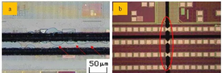
Fig. 1: Laser grooving defects (a) ILD peeling , (b) incomplete cut / discontinuities.
As a general guideline, for most wafers with the commonly used scribe features, the overlapping percentage is usually controlled between 60-90%. The calculation for overlapping percentage of the laser pulse is presented as in the equation below (J.C. Ion, 2005):
s : feed speed
d : laser beam diameter f : repetition frequency
On the other hand, the defocus amount parameter will influence the laser beam size that pass along the wafer surface, which will result in laser kerf width changes. Process optimisation of the combination of above mentioned parameters is required to reach the required kerf width, grooving depth and edge quality. In the process of laser grooving, the target grooving depth is typically only 10um to 15um, which is already sufficient to remove all the low k/ULK metallization with a good margin. The remaining of silicon is then separated through the following process of mechanical saw.
In order to accommodate both laser groove and blade dicing on a 120um scribe width, the maximum laser grooving kerf width allowable is between 70-76um. A dicing blade with the blade thickness in between 25um- 30um is selected for singulation the entire wafer with a step cut method. The best compromise between process cycle time and the grooving kerf quality, a designed 70-75um laser kerf width is established by using a 5-pass laser grooving process for a 300mm diameter wafer, and the wafer thickness is 280um.
In the 5-pass laser grooving process, the two outermost grooving lines are optimized for the best quality. Therefore, these lines are usually grooved with lowest laser power, but at a higher laser frequency and zero defocus. On the other hand, for the remaining inner lines, the parameters are tuned to give wider and deeper kerf depth, which can only be achieved by taking the lower repetition frequency that gives high laser power. The defocus setting of the center line is also the largest to achieve the widest kerf width possible. Some guidelines for parameter setting such as using the energy density method (Joules/cm2) is found to be useful as a baseline for optimization. The energy density equation is given as below (J.C. Ion, 2005):
P : average power
d : laser beam diameter
f : repetition frequency
RESULTS AND DISCUSSION
I. Topside Grooving Quality Inspection:
Fig. 2: Topside cutting quality comparison (a) blade dicing, (b) laser grooving.
II. Laser Groove Shape/Profile:
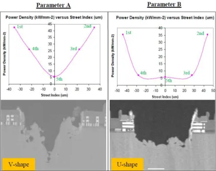
The results of using different laser process parameters can result in different grooving profiles and geometry. Fig. 3 presents the relationship between the power density (kW/mm-2) and the street index (um) using Parameter A and Parameter B. The graphical graph shows the outermost laser pass of the grooving (for 1st and 2nd laser pass) pose the highest power density; it’s intended to provide sufficient thermal energy to evaporate-off all the weaker and brittle ILD metal layers before proceeding to blade sawing. The lowest power density observed always at the center of the groove for the two laser parameter. The generated grooving geometry for Parameter A look like a typical V-shape groove. In fact, the grooving geometry for Parameter B looks like a U-shape groove, a typical bathtub shape when examined under SEM.
Fig. 3: Relationship between the power density (kW/mm-2) versus street index (um), using Parameter A and Parameter B.
III. Laser Groove Depth Inspection:
Fig. 4: Cross-sectional view of the produced laser groove depth for Parameter A and Parameter B.
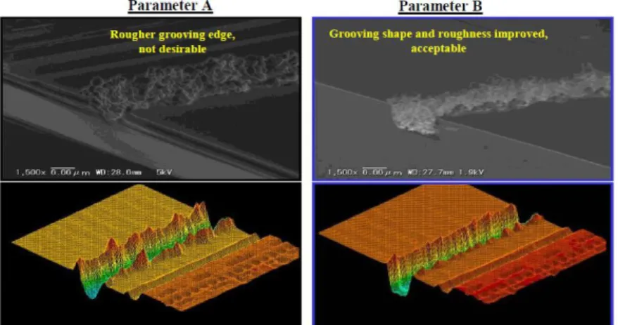
Fig. 5: Laser grooving edge quality and roughness inspection for Parameter A and Parameter B.
IV. Laser Grooving Defects and Challenges:
One of the most serious defects that was encountered during the laser process development is a hairline crack. It happens randomly along the laser kerf edge with no correlation to the scribe structures. The hairline cracks observed were in the range of 5-15um as illustrated in Fig. 6. Hairline crack does not look serious from the top view under low power optical scope. However, cross section into the defect by using FIB method revealed that the crack has indeed propagated and affected the low k/ULK metallization and circuitry. Under package stress test, this crack has a high possibility extending inward to the die and cause catastrophic failure. To resolve the hairline crack produced by the laser, process parameters fine tuning is needed by assessing all possible combination of critical process parameters (laser power, laser frequency, feed speed, and defocus amount) in order to obtain the optimum amount of energy density for 5-pass grooving.
Fig. 6: Laser grooving defect, hairline crack.
Fig. 7: SEM and optical photo of HAZ and dross adherence inside the groove.
Laser and blade saw kerf placement accuracy is crucial when comes to narrow saw scribe width wafer design. It’s important to avoid the mechanical blade from breaching into the side wall edges of the laser groove. Else, severe die topside ILD peeling and chipping can happen. A robust and effective in-line process control is necessary to reduce the chances of having off-center cutting for the mechanical blade dicing saw. Short kerf check (SKC) is an in-line process control tool used to trigger off-center dicing, and machine will stop for the user to make adjustment and correction. The problem can be resolved at an early stage before it was too late. Fig. 8 shows the blade saw kerf is off-center and result in peeling breach over to the die edge seal ring.
Fig. 8: Blade saw kerf damage the die side wall of the laser groove due to off-center cutting.
Other small cosmetic defects such as passivation peeling (Fig. 1a) and metal bulging (Fig. 9) due to laser process heat spread across the metal scribe structures are very common to see in laser grooving.
Fig. 9: Metal bulging due to laser grooving process heat transfer on the scribe structure.
Package reliability assessments were performed on the assembled dies which were processed with the optimized 5-pass laser parameters and diced with the step cut approach. No dicing related failures were found at time zero, after 4000 cycles of air-to-air temperature cycling (-65ºC /150ºC), and 192 hour HAST. Therefore, laser grooving and blade dicing was one of the potential solutions that significantly improved the dicing yield and reduced dicing defects for low k/ULK wafers.
Conclusions:
Therefore, laser grooving is possibly one of the best solutions for low-k/ULK wafer dicing, to improve the dicing quality and yield.
ACKNOWLEDGEMENT
The authors would like to thank LC Tan, and TSO-PAE engineers from Freescale Semiconductor (M) Sdn. Bhd., for providing technical assistance, guidance and supports. This project is funded by the Ministry of Higher Education (Grant Number: 2014109FRGS).
REFERENCES
Chaware, R., H. Lan, 2006. Reliability Improvement of 90nm Large Flip Chip Low-k Die via Dicing and Assembly Process Optimization, IEEE International Conference on Electronic Packaging Technology, page 622-626.
Cheung, T.A., 2005. Dicing Advanced Materials for Microelectronics, IEEE International Symposium on
Advanced Packaging Materials: Processes, Properties and Interfaces, page 149-152.
Dubey, A.K., V. Yadava, 2007. Optimization of Kerf Quality during Pulsed Laser Cutting of Aluminium Alloy Sheet, Journal of Materials Processing Technology, (204), page 412-418.
Efrat, U., 1993. Optimizing the Wafer Dicing Process, IEEE International Conference on Electronic
Manufacturing Technology, page 245-253.
Ion, J.C., 2005. Laser Processing of Engineering Materials: Principles, Procedure and Industrial. Massachusetts.
Koh, W.S., T.B. Lau, K.Y. Yow, 2009. Laser Grooving Characterization for Dicing Defects Reduction and its Challenges, IEEE International Conference on Electronic Packaging Technology, page 846-850.
Kumagai, M., N. Uchiyama, E. Ohmura, R. Sugiura, K. Atsumi, K. Fukumitsu, 2007. Advanced Dicing Technology for Semiconductor Wafer - Stealth Dicing, IEEE Transcations on Semiconductor Manufacturing, page 259-265.
Lau, T.B., Y.W. Lo, W.S. Koh, C.T. Siong, K.Y. Yow, 2008. Laser Grooving Process Development for Low-k / Ultra Low-k Devices, IEEE International Conference on Electronic Manufacturing Technology, page 1-6.
Lee, K.S., 2006. Laser as a Future Direction for Wafer Dicing: Parametric Study and Quality Assessment,
IEEE International Conference on Electronic Manufacturing Technology, page 506-509.
Tan, H.H., J. Beleran, Y.S. Koh, P.L. Ong, G. Mehta, G. Librado, X.R. Zhang, C. Surasit, 2011. Packaging Approach for Integrating 40/45-nm ELK Devices into Wire Bond and Flip-Chip Packages, IEEE Transactions
on Components, Packaging and Manufcaturing Technology, page 1923-1933.
Tran, T.A., V. Mathew, W.S. Koh, K.Y. Yow, Y.K. Au, 2012. Overcoming Dicing Challenges for Low-K Copper Wafers using Nickel-Palladium-Gold Bond Pads for Automotive Application, IEEE International
Conference on Electronic Manufacturing Technology, page 364-371.
Wang, Z.J., S. Wang, J.H. Wang, S. Lee, S.Y. Yao, R. Han, Y.Q. Su, 2005. 300mm Low-k Wafer Dicing Saw Study, IEEE International Conference on Electronic Packaging Technology, page 262-268.
Yibas, B.S., 2008. Laser Cutting of Thick Sheet Metals: Effects of Cutting Parameters on Kerf Size Variations, Journal of Materials Processing Technology, (201), page 285-290.
Yow, K.Y., W.S. Koh, 2010. Laser Grooving on Narrow Scribe Widths on Thick Flip Chip Wafer: The Challenges and its Resolution, IEEE International Conference on Electronic Packaging Technology, page 369-372.
Zhao, H., D. Shi, 2003. Process Challenges in Low-k Wafer Dicing, IEEE International Electronics