T
T
TS
S
S3
3
32
2
2G
G
G~
~
~1
1
12
2
28
8
8G
G
GP
P
PS
S
SD
D
D3
3
33
3
30
0
0
2.5” Solid State Disk
Transcend Information Inc.
V1.2 1
Description
Transcend PSD is a series of 2.5 PATA SSD with high performance and advanced flash control techniques. Due to smaller size (fit the standard dimensions of 2.5” IDE Hard Disk Drives), huge capacity, high speed, and low power consumption, Solid State Disk is perfect replacement storage device for PCs, Laptops, gaming systems, and handheld devices.
Placement
Features
• RoHS compliant products
• Supports LBA 48bit addressing.
• Fully compatible with devices and OS that support the IDE standard (44-Pin, pitch = 2.00 mm)
• Single Power Supply: 5V±10%
• Operating Temperature: 0oC to 70oC
• Storage Temperature: -40oC to 85oC
• Operating Humidity (Non condensation): 0% to 95%
• Storage Humidity (Non condensation): 0% to 95%
• Built-in ECC (Error Correction Code) functionality and global wear-leveling algorithm ensures highly reliable of data transfer
• True IDE Mode supports:
Ultra DMA Mode 0 to Ultra DMA Mode 6
MultiWord DMA Mode 0 to MultiWord DMA Mode 2
PIO Mode 0 to PIO Mode 4
• Shock resistance
• MTBF : 1,000,000 hours
• Support S.M.A.R.T (Self-defined) to monitor Erase Count for lifetime evaluation.
• Support Security Command
• Support Static Data Refresh, Early Retirement to extend product life
Dimensions
Side
Millimeters
Inches
A 100.30 ± 0.40 3.949 ± 0.016 B 69.85 ± 0.20 2.750 ± 0.008 C 7.40 ± 0.15 0.292 ± 0.004
T
T
TS
S
S3
3
32
2
2G
G
G~
~
~1
1
12
2
28
8
8G
G
GP
P
PS
S
SD
D
D3
3
33
3
30
0
0
2.5” Solid State Disk
Transcend Information Inc.
V1.2 2
Specifications
Capacity
Model P/N Cylinder Head Sector User LBA Physical Capacity
TS32GPSD330 16383 15 63 62,533,632 32,018,219,584 Byte
TS64GPSD330 16383 15 63 125,044,736 64,002,424,832 Byte
TS128GPSD330 16383 15 63 250,071,040 128,036,372,480 Byte
Note. PSD330 series is shipped with RAW format. Inquiry for formatted device please contact with sales/PM.
Performance
Sequential Read Sequential Write Random 4K Read Random 4K Write
32GB 119.0 36.12 13.86 1.276
64GB 114.7 63.92 11.42 1.252
128GB 118.4 92.75 13.09 1.225
Note : Test by Crystal Disk Mark V3.0.1, 500MB size @25 oC, P5K-VM(ICH 9), 1GB RAM * 2, IDE interface support up to UDMA6, Windows® XP SP3
Power consumption (mA)
Capacity 32GB 64GB 128GB
Read 240.9 236.8 240.1
Write 158.9 245.5 247.5
Idle 0.8 0.8 0.8
Note: All data above are maximum value from various test patterns.
Physical Specification
Form Factor 2.5-inch HDD
Storage Capacities 32 GB to 128 GB Dimensions (mm) Length 100.3 0 ± 0.40 Width 69.85 ± 0.20 Height 7.40 ± 0.15 Input Voltage 5V ± 10% Weight 55g ± 5g
T
T
TS
S
S3
3
32
2
2G
G
G~
~
~1
1
12
2
28
8
8G
G
GP
P
PS
S
SD
D
D3
3
33
3
30
0
0
2.5” Solid State Disk
Transcend Information Inc.
V1.2 3
Endurance
Capacity 32GB 64GB 128GB
Tera Byte Write 20 TBW 40 TBW 80 TBW
Note: Based on JEDEC JESD218A specification, Client Application Class. And based on the following scenario: Active use: 40oC, 8hrs/day; Retention use: 30oC 1year
Interface
Part Number Interface Transfer Mode Connector
TS32G~128GPSD330 True IDE mode
Ultra DMA mode 0~6 Multi-Word DMA Mode 0~2
PIO Mode 0 ~ 4
44pin 2mm pitch Pin male Header
Environmental Specifications
Operating Temperature 0oC to 70 oC
Storage Temperature -40 oC to 85 oC
Operating Humidity (Non condensation) 0% to 95%
Storage Humidity (Non condensation) 0% to 95%
Note: If Third party report is needed, please contact with sales/PM.
EMC/EMI
Compliance CE, FCC and BSMI
Note: If Third party report is needed, please contact with sales/PM.
SHOCK & Vibration Test
Condition Standard
Mechanical Shock Test 1500G, 0.5ms, 3 axes IEC 60068-2-27
Vibration Test 20G (Peak-to-Peak)
20Hz to 2000Hz (Frequency) IEC 60068-2-6
Interface Specification
Jumper Settings Master/Slave/Cable-select Settings
ATA Compatibility ATA/ATAPI 8
T
T
TS
S
S3
3
32
2
2G
G
G~
~
~1
1
12
2
28
8
8G
G
GP
P
PS
S
SD
D
D3
3
33
3
30
0
0
2.5” Solid State Disk
Transcend Information Inc.
V1.2 4
Package Dimensions
Below figure illustrates the Transcend 2.5” Solid State Disk. All dimensions are in mm.
Pin Assignments
Pin No. Pin Name Pin No. Pin Name
01 -RESET 02 GND 03 DD7 04 DD8 05 DD6 06 DD9 07 DD5 08 DD10 09 DD4 10 DD11 11 DD3 12 DD12 13 DD2 14 DD13 15 DD1 16 DD14 17 DD0 18 DD15 19 GND 20 KEY-PIN (OPEN) 21 DMARQ 22 GND 23 -DIOW : STOP 24 GND
25 -DIOR : -HDMARDY : HSTROBE 26 GND
27 IORDY : DDMARDY : DSTROBE 28 CSEL
29 -DMACK 30 GND
31 INTRQ 32 IOCS16B
33 DA1 34 -PDIAG : -CBLID
35 DA0 36 DA2 37 -CS0 38 -CS1 39 -DASP 40 GND 41 VCC 42 VCC 43 GND 44 NC (No Connect) Pin Layout
Reliability
1. Global Wear Leveling – Advanced algorithm to enhance the Wear-Leveling Efficiency
There are 3 main processes in SMI global wear leveling approaches:
A. Record the block erase count and save in the wear-leveling table.
B. Find the static-block and save it in wear-leveling pointer.
C. Check the erase count when the block popped from spare pool. If the block erase count is bigger than WEARCNT, then it swapped the static-block and over-count-block.
After actual test, global wear leveling successfully even the erase count of every block; hence, it can extend the life expectancy of Flash product.
2. StaticDataRefresh Technology – Keeping Data Healthy
In the MLC technology, multiple charge levels are used to store data. There are many variants that would disturb the charge inside a Flash cell. These variants can be: time, read operations, undesired charge, heat, etc; each variant would create a charge loss, and the contents shift in their charge levels slightly. In our everyday usage – more than 60% are repeated read operations, the accumulated charge loss would eventually result in the data loss.
Normally, ECC engine corrections are taken place without affecting the host normal operations. As time passes by, the number of error bits accumulated in the read transaction exceeds the correcting capability of the ECC engine, resulting in corrupted data being sent to the host.
To prevent this, Transcend’s SPD330 monitor the error bit levels at each read operation; when it reaches the preset threshold value, the controller automatically performs data refresh to “restore” the correct charge levels in the cell. This implementation practically restores the data to its original, error-free state, and hence, lengthening the life of the data.
3. EarlyRetirement – Avoiding Data Loss Due to Weak Block.
The StaticDataRefresh feature functions well when the cells in a block are still healthy. As the block ages over time, it cannot store charge reliably anymore, EarlyRetirement enters the scene.
EarlyRetirement works by moving the static data to another block (a health block) before the previously used block becomes completely incapable of holding charges for data. When the charge loss error level exceeds another threshold value (higher from that for StaticDataRefresh), the controller automatically moves its data to another block. In addition, the original block is then marked as a bad block, which prevents its further use, and thus the block enters the state of “EarlyRetirement.” Note that, through this process, the incorrect data are detected and effectively corrected by the ECC engine, thus the data in the new block is stored error-free.
4. Advanced Power Shield – Avoiding Data Loss during Power Failure
When a power failure takes place, the line voltage drops. When it reaches the first Logic-Freeze Threshold, the core controller is held at a steady state. Here are some implications. First, it ceases the communication with the host. This
prevents the host from sending in further address/instructions/data that may be corrupted. During power disturbance, the host is likely experiencing a voltage drop, so the transmission integrity cannot be guaranteed. Second, it stops the information sending to the Flash. This prevents the controller from corrupting the address/data being transmitted to the Flash, and corrupting the Flash contents inadvertently.
Further more, Advanced Power Shield cut off the connection between host power and turn off the controller to reserve most of the energy for NAND Flash to complete programming. Due to MLC structure, an interrupted programming may damage a paired page which cause the previous written data lost.
Note:Transcend does not guarantee that data can be protected by Power Shield/ Advanced Power Shield under all conditions.
Support ATA/ATAPI Command List
Support ATA/ATAPI Command Code Protocol
General Feature Set
EXECUTE DIAGNOSTICS 90h Device diagnostic
FLUSH CACHE E7h Non-data
IDENTIFY DEVICE ECh PIO data-In
READ DMA C8h DMA
READ MULTIPLE C4h PIO data-In
READ SECTOR(S) 20h PIO data-In
READ VERIFY SECTOR(S) 40h or 41h Non-data
SET FEATURES EFh Non-data
SET MULTIPLE MODE C6h Non-data
WRITE DMA CAh DMA
WRITE MULTIPLE C5h PIO data-out
WRITE SECTOR(S) 30h PIO data-out
NOP 00h Non-data
READ BUFFER E4h PIO data-In
WRITE BUFFER E8h PIO data-out
Power Management Feature Set
CHECK POWER MODE E5h or 98h Non-data
IDLE E3h or 97h Non-data
IDLE IMMEDIATE E1h or 95h Non-data
SLEEP E6h or 99h Non-data
STANDBY E2h or 96h Non-data
STANDBY IMMEDIATE E0h or 94h Non-data
Security Feature Set
SECURITY SET PASSWORD F1h PIO data-out
SECURITY UNLOCK F2h PIO data-out
SECURITY ERASE PREPARE F3h Non-data
SECURITY ERASE UNIT F4h PIO data-out
SECURITY FREEZE LOCK F5h Non-data
SECURITY DISABLE PASSWORD F6h PIO data-out
SMART Feature Set
SMART Disable Operations B0h Non-data
SMART Enable/Disable Autosave B0h Non-data
SMART Enable Operations B0h Non-data
SMART Return Status B0h Non-data
SMART Execute Off-Line Immediate B0h Non-data
SMART Read Data B0h PIO data-In
Host Protected Area Feature Set
Read Native Max Address F8h Non-data
Set Max Address F9h Non-data
Set Max Set Password F9h PIO data-out
Set Max Lock F9h Non-data
Set Max Freeze Lock F9h Non-data
General Feature Set
FLUSH CACHE (E7h)
This command is used by the host to request the device to flush the write cache. If there is data in the write cache, that data shall be written to the media. The BSY bit shall remain set to one until all data has been successfully written or an error occurs.
IDENTIFY DEVICE (ECh)
This commands read out 512 Bytes of drive parameter information. Parameter Information consists of the arrangement and value as shown in the following table. This command enables the host to receive the Identify Drive Information from the device.
Identify Device Information Default Value
Word Address Default value
(Hex) Total Bytes Data Field Type Information
0 0x044A 2 General configuration
1 0xXXXX 2 Default number of cylinders
2 0x0000 2 Reserved
3 0x00XX 2 Default number of heads
4-5 0x02400000 4 Obsolete
6 0xXXXX 2 Default number of sectors per track
7 - 8 0xXXXXXXXX 4 Number of sectors per card (Word 7 = MSW, Word 8 = LSW)
9 0x0000 2 Obsolete
10 - 19 0xXXXX 20 Serial number in ASCII (Right justified)
20 0x0002 2 Obsolete
21 0x0002 2 Obsolete
22 0x0000 2 Obsolete
23 - 26 0xXXXX 8 Firmware revision in ASCII.
Big Endian Byte Order in Word
27 - 46 0xXXXX 40 Model number in ASCII (Left justified). Big Endian Byte Order in Word.
47 0x8001 2 Maximum number of sectors on Read/Write Multiple command
48 0x0000 2 Reserved
49 0x0F00 2 Capabilities
50 0x0000 2 Reserved
51 0x0200 2 PIO data transfer cycle timing mode
52 0x0000 2 Obsolete
53 0x0007 2 Field validity
54 0xXXXX 2 Current numbers of cylinders
55 0xXXXX 2 Current numbers of heads
56 0xXXXX 2 Current sectors per track
57 - 58 0xXXXX 4 Current capacity in sectors (LBAs) (Word57 = LSW , Word58 = MSW)
59 0x0000 2 Multiple sector setting
60 - 61 0xXXXX 4 Total number of sectors addressable in LBA Mode
Word Address
Default value
62 0x0000 2 Reserved
63 0x0007 2 Multiword DMA transfer
64 0x0003 2 Advanced PIO modes supported
65 0x0078 2 Minimum Multiword DMA transfer cycle time per word 66 0x0078 2 Recommended Multiword DMA transfer cycle time. 67 0x0078 2 Minimum PIO transfer cycle time without flow control 68 0x0078 2 Minimum PIO transfer cycle time with lORDY flow control
69 -79 0x0000 22 Reserved
80 0x0800 2 Major version number (ATAPI-8)
81 0x0000 2 Minor version number
82 0x7028 2 Command sets supported 0
83 0x5000 2 Command sets supported 1
84 0x4000 2 Command sets supported 2
85 0x0000 2 Command sets enabled 0
86 0x0000 2 Command sets enabled 1
87 0x0000 2 Command sets enabled 2
88 0x007F 2 Ultra DMA mode supported and selected
89 0x0000 2 Time required for Security erase unit completion
90 0x0000 2 Time required for Enhanced security erase unit completion
91 0x0000 2 Current Advanced power management value
92 0x0000 3 Master Password Revision Code
93
0x604F 0x6F00 0x603F
2
‧ Hardware reset result (Master only) ‧ Hardware reset result (Slave only)
‧ Hardware reset result (Master w/ slave present)
94 - 127 0x0000 68 Reserved
128 0x0001 2 Security Status
129-159 0xXXXX 62 Vendor specific
160 0x0000 2 Power requirement description
161 0x0000 2 Reserved
162 0x0000 2 Key management schemes support
163 0x0000 2 CF Advanced True IDE Timing Mode Capability and Setting
164 0x0000 2
‧CF Advanced PCMCIA I/O and Memory Timing Mode Capability and Setting
‧80 ns cycle in memory and I/O mode
165 - 175 0x0000 22 Reserved
176 - 255 0x0000 160 Reserved
READ DMA (C8h)
Read data from sectors during Ultra DMA and Multiword DMA transfer. Use the SET FEATURES command to specify the mode value. A sector count of zero requests 256 sectors.
READ MULTIPLE (C4h)
This command performs similarly to the Read Sectors command. Interrupts are not generated on each sector, but on the transfer of a block which contains the number of sectors defined by a Set Multiple command.
READ SECTOR(S) (20h)
This command reads 1 to 256 sectors as specified in the Sector Count register from sectors which is set by Sector number register. A sector count of 0 requests 256 sectors. The transfer beings specified in the Sector Number register.
READ VERIFY SECTOR(S) (40h/41h)
This command verifies one or more sectors on the drive by transferring data from the flash media to the data buffer in the drive and verifying that the ECC is correct. This command is identical to the Read Sectors command, except that DRQ is never set and no data is transferred to the host.
SET FEATURES (EFh)
This command set parameter to Features register and set drive’s operation. For transfer mode, parameter is set to Sector Count register. This command is used by the host to establish or select certain features.
SET MULTIPLE MODE (C6h)
This command enables the device to perform READ MULTIPLE and WRITE MULTIPLE operations and establishes the block count for these commands.
WRITE DMA (CAh)
Write data to sectors during Ultra DMA and Multiword DMA transfer. Use the SET FEATURES command to specify the mode value.
WRITE MULTIPLE (C5h)
This command is similar to the Write Sectors command. Interrupts are not presented on each sector, but on the transfer of a block which contains the number of sectors defined by Set Multiple command.
WRITE SECTOR(S) (30h)
Write data to a specified number of sectors (1 to 256, as specified with the Sector Count register) from the specified address. Specify “00h” to write 256 sectors.
NOP (00h)
The device shall respond with command aborted. For devices implementing the Overlapped feature set, subcommand code 00h in the Features register shall abort any outstanding queue. Subcommand codes 01h through FFh in the Features register shall not affect the status of any outstanding queue.
READ BUFFER (E4h)
The READ BUFFER command enables the host to read a 512-byte block of data.
WRITE BUFFER (E8h)
This command enables the host to write the contents of one 512-byte block of data to the device’s buffer.
Power Management Feature Set
CHECK POWER MODE (E5h or 98h)
IDLE (E3h or 97h)
This command causes the device to set BSY, enter the Idle mode, clear BSY and generate an interrupt. If sector count is non-zero, the automatic power down mode is enabled. If the sector count is zero, the automatic power mode is disabled.
IDLE IMMEDIATE (E1h or 95h)
This command causes the device to set BSY, enter the Idle(Read) mode, clear BSY and generate an interrupt.
SLEEP (E6h or 99h)
This command causes the device to set BSY, enter the Sleep mode, clear BSY and generate an interrupt.
STANDBY (E2h or 96h)
This command causes the device to set BSY, enter the Sleep mode (which corresponds to the ATA “Standby” Mode), clear BSY and return the interrupt immediately.
STANDBY IMMEDIATE (E0h or 94h)
This command causes the drive to set BSY, enter the Sleep mode (which corresponds to the ATA “Standby” Mode), clear BSY and return the interrupt immediately.
Security Mode Feature Set
SECURITY SET PASSWORD (F1h)
This command set user password or master password. The host outputs sector data with PIO data-out protocol to indicate the information defined in the following table.
Security set Password data content1
Word Content 0 Control word Bit 0 Bits 1-7 Bit 8 Bits 9-15 Identifier Reserved Security level Reserved
0=set user password 1=set master password
0=High 1=Maximum
1-16 Password (32 bytes) 17-255 Reserved
SECURITY UNLOCK (F2h)
This command disables LOCKED MODE of the device. This command transfers 512 bytes of data from the host with PIO data-out protocol. The following table defines the content of this information.
Security Unlock information2
Word Content 0 Control word Bit 0 Bits 1-15 Identifier Reserved
0=compare user password 1=compare master password
1-16 Password (32 bytes) 17-255 Reserved
SECURITY DISABLE PASSWORD (F6h)
Disables any previously set user password and cancels the lock. The host transfers 512 bytes of data, as shown in the following table, to the drive. The transferred data contains a user or master password, which the drive compares with the saved password. If they match, the drive cancels the lock. The master password is still saved. It is re-enabled by issuing the SECURITY SET PASSWORD command to re-set a user password.
SECURITY ERASE PREPARE (F3h)
This command shall be issued immediately before the Security Erase Unit command to enable erasing and unlocking. This command prevents accidental loss of data on the drive.
SECURITY ERASE UNIT (F4h)
The host uses this command to transfer 512 bytes of data, as shown in the following table, to the drive. The transferred data contains a user or master password, which the drive compares with the saved password. If they match, the drive deletes user data, disables the user password, and cancels the lock. The master password is still saved. It is re-enabled by issuing the SECURITY SET PASSWORD command to re-set a user password.
SECURITY FREEZE LOCK (F5h)
Causes the drive to enter Frozen mode. Once this command has been executed, the following commands to update a lock result in the Aborted Command error:
• SECURITY SET PASSWORD • SECURITY UNLOCK
• SECURITY DISABLE PASSWORD • SECURITY ERASE PREPARE • SECURITY ERASE UNIT
The drive exits from Frozen mode upon a power-off or hard reset. If the SECURITY FREEZE LOCK command is issued when the drive is placed in Frozen mode, the drive executes the command, staying in Frozen mode.
Transcend IDE SSD supports the SMART command set and define some vendor-specific data to report spare/bad block numbers in each memory management unit. Individual SMART commands are identified by the value placed in the Feature register. Table shows these Feature register values.
SMART Feature Register Values
D0h Read Data D5h Reserved
D1h Read Attribute Threshold D6h Reserved
D2h Enable/Disable Autosave D8h Enable SMART Operations D3h Save Attribute Values D9h Disable SMART Operations D4h Execute OFF-LINE Immediate DAh Return Status
SMART DISABLE OPERATIONS
B0h with a Feature register value of D9h.Disables the SMART function. Upon receiving the command, the drive disables all SMART operations. This setting is maintained when the power is turned off and then back on.
Once this command has been received, all SMART commands other than SMART ENABLE OPERATIONS are aborted with the Aborted Command error.
This command disables all SMART capabilities including any and all timer and event count functions related
exclusively to this feature. After command acceptance, this controller will disable all SMART operations. SMART data in no longer be monitored or saved. The state of SMART is preserved across power cycles.
SMART ENABLE/DISABLE ATTRIBUTE AUTOSAVE
B0h with a Feature register value of D2h.Enables or disables the attribute value autosave function. This command specifies whether the current attribute values are automatically saved to the drive when it changes the mode. This setting is maintained when the power is turned on and off.
SMART ENABL OPERATIONS
B0h with a Feature register value of D8h.Enables the SMART function. This setting is maintained when the power is turned off and then back on. Once the SMART function is enabled, subsequent SMART ENABLE OPERATIONS commands do not affect any parameters
SMART EXECUTE OFF-LINE IMMEDIATE
B0h with the content of the Features register equal to D4h. This command causes the device to immediately initiate the optional set of activities that collect SMART data in an off-line mode and then save this data to the device's non-volatile memory, or execute a self-diagnostic test routine in either captive or off-line mode.
SMART RETURN STATUS
B0h with a Feature register value of DAh. This command causes the device to communicate the reliability status of the device to the host. If a threshold exceeded condition is not detected by the device, the device shall set the LBA Mid register to 4Fh and the LBA High register to C2h. If a threshold exceeded condition is detected by the device, the device shall set the LBA Mid register to F4h and the LBA High register to 2Ch.
B0h with the content of the Features register equal to D0h. This command returns the Device SMART data structure to the host.
SMART DATA Structure
The following 512 bytes make up the device SMART data structure. Users can obtain the data by SMART command.
BYTE F / V Description
0-1 X Revision code
2-361 X Vendor specific
362 V Off-line data collection status 363 X Self-test execution status byte
364-365 V Total time in seconds to complete off-line data collection activity
366 X Vendor specific
367 F Off-line data collection capability 368-369 F SMART capability
370 F
Error logging capability 7-1 Reserved
0 1=Device error logging supported
371 X Vendor specific
372 F Short self-test routine recommended polling time (in minutes) 373 F Extended self-test routine recommended polling time (in minutes) 374 F Conveyance self-test routine recommended polling time (in minutes)
375-385 R Reserved
386-395 F Firmware Version/Date Code
396-399 R Reserved
400-406 F ‘SMI2236’
407-511 R Reserved
F=the content of the byte is fixed and does not change.
V=the content of the byte is variable and may change depending on the state of the device or the commands executed by the device.
X=the content of the byte is vendor specific and may be fixed or variable. R=the content of the byte is reserved and shall be zero.
SMART Attributes
The following table defines the vendor specific data in byte 2 to 361 of the 512-byte SMART data.
Attribute
ID(hex) Raw Attribute Value Attribute Name
01 MSB 00 00 00 00 00 Read Error Rate
05 LSB MSB 00 00 00 00 Reallocated Sectors Count
0C LSB MSB 00 00 00 00 Power Cycle Count
A1 LSB MSB 00 00 00 00 Number of Valid Spare Block A2 LSB MSB 00 00 00 00 Number of child pair
A3 LSB MSB 00 00 00 00 Number of initial invalid Block
A4 LSB ~ ~ MSB 00 00 Total erase count
A5 LSB ~ ~ MSB 00 00 Maximum Erase Count
A6 LSB ~ ~ MSB 00 00 Minimum Erase Count
A7 LSB ~ ~ MSB 00 00 Average Erase Count
C0 LSB MSB 00 00 00 00 Power-Off Retract Count C7 LSB MSB 00 00 00 00 Ultra DMA CRC Error Rate
Host Protected Area Feature Set
A reserved area for data storage outside the normal operating system file system is required for several specialized applications. Systems may wish to store configuration data or save memory to the device in a location that the operating systems cannot change. The optional Host Protected Area feature set allows a portion of the device to be reserved for such an area when the device is initially configured.
Ultra DMA data transfer
Ultra DMA data burst timing requirements Name Mode 0 (in ns) Mode 1 (in ns) Mode 2 (in ns) Mode 3 (in ns) Mode 4 (in ns) Mode 5 (in ns) Mode 6 (in ns) Measurement location
Min Max Min Max Min Max Min Max Min Max Min Max Min Max
t2CYCTYP 240 160 120 90 60 40 30 Sender tCYC 112 73 54 39 25 16.8 13.0 Note 3 t2CYC 230 153 115 86 57 38 29 Sender tDS 15.0 10.0 7.0 7.0 5.0 4.0 2.6 Recipient tDH 5.0 5.0 5.0 5.0 5.0 4.6 3.5 Recipient tDVS 70.0 48.0 31.0 20.0 6.7 4.8 4.0 Sender tDVH 6.2 6.2 6.2 6.2 6.2 4.8 4.0 Sender tCS 15.0 10.0 7.0 7.0 5.0 5.0 5.0 Device tCH 5.0 5.0 5.0 5.0 5.0 5.0 5.0 Device tCVS 70.0 48.0 31.0 20.0 6.7 10.0 10.0 Host tCVH 6.2 6.2 6.2 6.2 6.2 10.0 10.0 Host tZFS 0 0 0 0 0 35 25 Device tDZFS 70.0 48.0 31.0 20.0 6.7 25 17.5 Sender tFS 230 200 170 130 120 90 80 Device tLI 0 150 0 150 0 150 0 100 0 100 0 75 0 60 Note 4 tMLI 20 20 20 20 20 20 20 Host tUI 0 0 0 0 0 0 0 Host tAZ 10 10 10 10 10 10 10 Note 5 tZAH 20 20 20 20 20 20 20 Host tZAD 0 0 0 0 0 0 0 Device tENV 20 70 20 70 20 70 20 55 20 55 20 50 20 50 Host tRFS 75 70 60 60 60 50 50 Sender tRP 160 125 100 100 100 85 85 Recipient tIORDYZ 20 20 20 20 20 20 20 Device tZIORDY 0 0 0 0 0 0 0 Device tACK 20 20 20 20 20 20 20 Host tSS 50 50 50 50 50 50 50 Sender
Name Comment
t2CYCTYP Typical sustained average two cycle time
tCYC Cycle time allowing for asymmetry and clock variations (from STROBE edge to STROBE edge)
t2CYC Two cycle time allowing for clock variations (from rising edge to next rising edge or from falling edge to next
falling edge of STROBE)
tDS Data setup time at recipient (from data valid until STROBE edge)
tDH Data hold time at recipient (from STROBE edge until data may become invalid)
tDVS Data valid setup time at sender (from data valid until STROBE edge)
tDVH Data valid hold time at sender (from STROBE edge until data may become invalid)
tCS CRC word setup time at device
tCH CRC word hold time device
tCVS CRC word valid setup time at host (from CRC valid until DMACK- negation)
tCVH CRC word valid hold time at sender (from DMACK- negation until CRC may become invalid)
tZFS Time from STROBE output released-to-driving until the first transition of critical timing.
tDZFS Time from data output released-to-driving until the first transition of critical timing.
tFS First STROBE time (for device to first negate DSTROBE from STOP during a data in burst)
tLI Limited interlock time
tMLI Interlock time with minimum
tUI Unlimited interlock time
tAZ Maximum time allowed for output drivers to release (from asserted or negated)
tZAH Minimum delay time required for output
tZAD drivers to assert or negate (from released)
tENV Envelope time (from DMACK- to STOP and HDMARDY- during data in burst initiation and from DMACK to
STOP during data out burst initiation)
tRFS Ready-to-final-STROBE time (no STROBE edges shall be sent this long after negation of DMARDY-)
tRP Ready-to-pause time (that recipient shall wait to pause after negating DMARDY-)
tIORDYZ Maximum time before releasing IORDY
tZIORDY Minimum time before driving IORDY
tACK Setup and hold times for DMACK- (before assertion or negation)
Sustained Ultra DMA data-in burst
Sustained Ultra DMA data-out burst
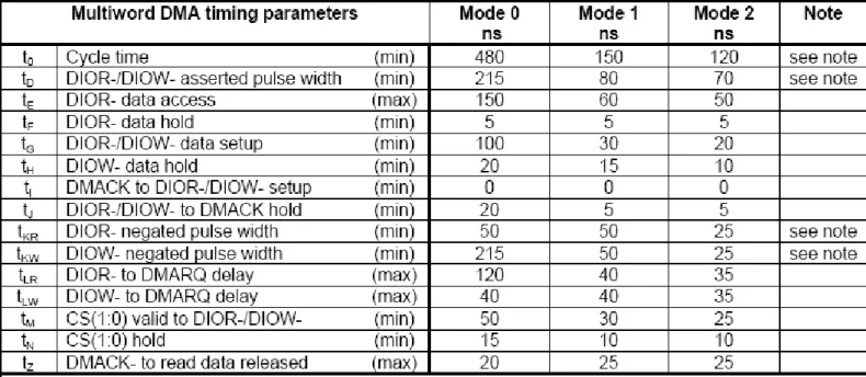
Multiword DMA data transfer
For Multiword DMA modes 1 and above, the minimum value of t0 is specified by word 65 in the IDENTIFY DEVICE parameter list. Table 50 defines the minimum value that shall be placed in word 65. Devices shall power-up with mode 0 as the default Multiword DMA mode.
PIO data transfer
PIO timing requirements
PIO timing parameters Mode 0
ns Mode 1 ns Mode 2 ns Mode 3 ns Mode 4 ns
t0 Cycle time (min) 600 383 240 180 120
t1 Address valid to DIOR-/DIOW- setup (min) 70 50 30 30 25
t2 DIOR-/DIOW- (min) 165 125 100 80 70
t2i DIOR-/DIOW- recovery time (min) - - - 70 25
t3 DIOW- data setup (min) 60 45 30 30 20
t4 DIOW- data hold (min) 30 20 15 10 10
t5 DIOR- data setup (min) 50 35 20 20 20
t6 DIOR- data hold (min) 5 5 5 5 5
t6Z DIOR- data tristate (max) 30 30 30 30 30
t9 DIOR-/DIOW- to address valid hold (min) 20 15 10 10 10
tRD
Read Data Valid to IORDY active (if IORDY initially low after tA)
(min) 0 0 0 0 0
tA IORDY Setup time 35 35 35 35 35
tB IORDY Pulse Width (max) 1250 1250 1250 1250 1250
Ordering Information
The above technical information is based on industry standard data and has been tested to be reliable. However, Transcend makes no warranty, either expressed or implied, as to its accuracy and assumes no liability in connection with the use of this product. Transcend reserves the right to make changes to the specifications at any time without prior notice.
USA Los Angeles: E-mail: [email protected] Maryland: E-mail: [email protected] www.transcendusa.com CHINA E-mail: [email protected] www.transcendchina.com TAIWAN
No.70, XingZhong Rd., NeiHu Dist., Taipei, Taiwan, R.O.C TEL +886-2-2792-8000 Fax +886-2-2793-2222 E-mail: [email protected] www.transcend.com.tw GERMANY E-mail: [email protected] www.transcend.de HONG KONG E-mail: [email protected] www.transcendchina.com JAPAN E-mail: [email protected] www.transcend.jp THE NETHERLANDS E-mail: [email protected] www.transcend.nl United Kingdom E-mail: [email protected] www.transcend-uk.com KOREA
E-mail: [email protected]