High Performance Broadband integrated GaAs
Electro-Optic Absorption Modulators With Distributed
Feedback Lasers in Optical Transmission Engineering
Systems
Ahmed Nabih Zaki RashedElectronics and Electrical Communications Engineering Department Faculty of Electronic Engineering, Menouf 32951, Menoufia University, EGYPT
E-mail: [email protected]
Abstract— For high bit rates and long haul optical communication systems using a single-mode fiber, a modulator with low chirp and small size are demanded. An electro-absorption modulator is very attractive because it has some advantages of not only low chirp and small size but also the elimination of polarization control through monolithic integration with a distributed feedback (DFB) laser. The modulation bandwidth of traditional lumped electro-absorption modulators (EAMs) is usually limited by the RC time constant, but the effective resistance R and capacitance C are not easily extracted for advanced device geometries. This paper has presented the important transmission characteristics of EA modulators such as transmission performance efficiency, insertion loss, extinction ratio, , over wide range of the affecting parameters for different selected electro-absorption materials to be the major of interest.
Index Terms— GaAs semiconductor material, Electro absorption modulator, and High Speed switching applications.
I.INTRODUCTION
Silicon photonics has become a very attractive research area in the past decade due to the potential of monolithically integrating photonic devices with complementary-metal-oxide-semiconductor (CMOS) microelectronic circuits on this platform [1]. Such an integration approach is crucial for the successful realization of next generation low cost optical links for data COM and Tele COM applications, and has further application potential in areas such as chemical and biochemical sensing. Recently interest is increasing in the integration of optical links into microprocessors to facilitate high performance and low-cost super computing [2]. Significant research effort in this area, has led to the demonstration of essential building-block components, including silicon based lasers [3], photo detectors [4], and modulators [5]. Among these, high speed silicon based modulators are critical components that have proved difficult to realize in practical devices. Owing to the weak electro-optical effect of silicon, most demonstrated waveguide based silicon modulators utilize the free carrier dispersion effect [6]. The fastest silicon modulator demonstrated uses this effect and operates at 40Gb/s but has a limited extinction ratio of 1dB. To achieve an acceptable extinction ratio, the device is usually a few millimeters long and works at 6-10 V reverse bias because of the weak free carrier effect. The power consumption of this type of device is in the order of a few hundred miliwalts. Recently, Ref. [7] demonstrated a waveguide integrated Ge Si modulator based
on the electro-absorption (EA) effect with 1.2 GHz modulation speed. The EA effect is known as the Franz-Keldysh (FK) effect in bulk semiconductors and the quantum-confined Stark effect (QCSE) in quantum-well (QW) structures [7].
Electro-Absorption Modulators (EAMs) are among the most important components of high-speed Wavelength Division Multiplexing (WDM) optical communications devices and systems. EAM are widely used as stand alone devices [8], as part of Electro-Absorption Modulated Lasers (EML), and as part of multi-component Planar Lightwave Circuits (PLC). Since the first proposed EAM based on optical absorption of light in a bulk structure more than two decades ago, advances have been made in modulator performances such as extinction ratio, polarization insensitivity, and bandwidth. Multiple Quantum Well (MQW) structures in the active region have become the structures of choice for EAM due to their improved extinction and reduced polarization sensitivity through applied strain [9]. While lumped electrode devices have demonstrated performance at rates of 10 Gb/s and higher, the more recent traveling wave electrode devices have been shown to work at rates of 43 Gb/s and above. Compared to the other popular class of modulators, Mach Zehnder based Lithium Niobate modulators, EAM offer a number of advantages such as low voltage drive, small size, high bandwidth, and potential for monolithic integration with other optoelectronic devices. For good performance of the modulator, a high extinction ratio is necessary. The vast majority of all designed and fabricated EAM employ a straight section of single-mode waveguide where optical absorption takes place under a bias voltage.
II.DEVICE MODELING
Based on MATLAB curve fitting program, the relation between modulator transmission (Tm) and the applied bias voltage can be estimated by the following expression [10]:
3 3 2
2
0312 . 0 00432
. 0 654 .
0 B B B
m V V V
T (1)
As well as the relations between extinction ratio (ER) and insertion loss (IL) and operating signal wavelength, applied bias voltage can be estimated by the following [11]:
3 3 2
2 1.654 00543
. 0 0324 .
0 VB VB VB
ER (2)
3 3 2
2 0.00654 543
. 1 732 .
0 VB VB VB
IL (3)
01.3243VB0.0654332VB20.005443VB3 (4)
3 3 2
2 0.05875 00365
. 0 654 .
3 VB VB VB
G (5)
The output power of the modulator can be given by the mathematical equation [13]:
) ( exp 0 m S
out P L
P (6)
The effective index of the mode obtained from the optical simulation is used to calculate the transmittance of an optical signal through the modulator or modulation efficiency ηm using the following equations:
Lm
m
exp (7)
/ 4
ng neff T (8)
Where α denotes the power absorption coefficient, Lm is the length of the device, ng is the group index of the waveguide, neff is the effective index, λ is the wavelength of operation. The first term of Eq. (8) essentially accounts for the slowed propagation of the light due to the reduced group velocity of the mode in the waveguide. This term is important in nano sized waveguides because the group index is significantly larger than the effective index of the mode [14, 15]. The effective and group index are calculated using the mode solver and the well known equation:
2 4 3 2 2 1 2
C C
C C
neff
(9) d dn n
ng eff eff (10)
The set of parameters is recast and dimensionally adjusted as [15]: C1= 8.906, C2= 2.3501, C3=c3T2; c3= (0.25286/T0)2, and C4=c4 (1.921+ 0.257x10⁻⁴T); c4=0.03454. Then the first and second differentiation of above empirical eq. (9) with respect to operating optical signal wavelength, λ that gives:
2 4
3 2 2 C C C n d dn eff eff (11)
Based on curve fitting MATLAB program, the fitting relation between confinement , bias voltage and operating optical signal wavelength by the following formula [16-19]:
3 3 2
2 0.0321 65433
. 0 0654 .
0 VB VB VB
(12)
The input resistance can be further reduced using multiple vias with a tradeoff of more insertion loss [20, 21]:
R=ρ Lm/A (13)
Where ρ is the resistivity, Lm is the modulator length and A=tW is the contact area (thickness x width). The time constant of the device and switching speed can be calculated as follows [22]:
τ=R CLaser (14)
laser RC SS 2 1
(15)
The relation between power length product and switching speed for electro-absorption materials can be estimated based on MATLAB curve fitting program [23]:
3 2 0654 . 1 65 . 1 54 .
2 SS SS SS
PLP (16)
The relative refractive index difference Δn can be estimated by the following formula:
m B eff L V r n n 41 3 5 . 0
(17)
Therefore the optimum length for GaAs electro-optic absorption modulator can be given by [24]:
n Lopt
0.5
. (18)
The modulator phase shift Δφ can be expressed as the following formula [25]:
nLm
2 (19)
The modulation bandwidth Δfm can be estimated by the following expression [26]:
m m RC
f 0.7
(20)
Where the capacitance of modulator device can be estimated by the following formula [27]:
Cm= t L c m r 0 (21)
Lastly, the modulator temperature coefficient rise (degree C/μm) can be given by [28, 29]:
dT dn L T eff m m 2
(22)
III.SIMULATION RESULTS AND PERFORMANCE ANALYSIS The model has been investigated high performance broadband integrated electro optic absorption modulators in high speed optical fiber communication systems over wide range of the affecting operating parameters as shown in Table 1.
Table 1: Parameters for electro-absorption modulators [3, 6, 9, 22].
Parameter Definition Value and unit
T0 Room temperature 300 K
Lm Modulator length 100 μm-500 μm
W Modulator width 50 μm-200 μm
t Modulator thickness 25 nm-100 nm
Ps Input signal power 100 mWatt—500
mWatt
Operating signal wavelength 1300 nm—1550 nm
r41 Electro-optic coefficient 1.4x10⁻¹⁰ cm/Volt
VB Applied bias voltage 0 Volt—5 Volt
εr Relative permittivity 1.65
c Speed of light 3x10⁸ m/sec
ε0 Free space permittivity 8.854x10⁻¹² F/cm
T Ambient temperature 300 K-400 K
ρ Resistivity 2.65x10⁹ ohm.cm
CLaser Input laser capacitance 0.5 nF
Based on the model equations analysis, assumed set of the operating parameters, and the set of the series of the Figs. (1-18), the following facts are assured:
ii) Fig. 2 has demonstrated that modulator extinction ratio increases with increasing both operating optical signal wavelength and decreasing applied bias voltage.
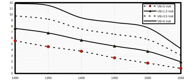
iii) Figs. (3, 4) have indicated that modulator insertion loss and intrinsic modal absorption decreases with increasing both operating optical signal wavelength and decreasing applied bias voltage.
iv) Fig. 5 has assured that modulator gain increases with increasing operating optical signal wavelength and decreasing applied bias voltage.
v)Figs. (6, 7) have demonstrated that modulator output power increases with increasing both operating optical signal wavelength and applied bias voltage while decreasing of modulator length.
vi) Figs. (8, 9) have proved that modulation efficiency increases with increasing operating optical signal wavelength while decreasing of modulator length and surrounding ambient temperature.
vii) Fig. 10 has demonstrated that modulator confinement increases with decreasing both operating optical signal wavelength and decreasing applied bias voltage.
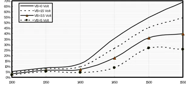
0% 5% 10% 15% 20% 25% 30% 35% 40% 45% 50% 55% 60% 65% 70%
1300 1350 1400 1450 1500 1550
VB=0 Volt VB=1.5 Volt VB=3.5 Volt VB=5 Volt
Operating optical signal wavelength, λ, μm
Fig. 1. Modulator transmission in relation to applied bias voltage and operating optical signal wavelength at the assumed set of the operating parameters.
0 0.5 1 1.5 2 2.5 3 3.5 4 4.5 5 5.5 6 6.5 7
1300 1350 1400 1450 1500 1550
VB=0 Volt VB=1.5 Volt VB=3.5 Volt VB=5 Volt
Operating optical signal wavelength, λ, μm
Fig. 2. extinction ratio in relation to applied bias voltage and operating optical signal wavelength at the assumed set of th e operating parameters.
M
od
ul
at
o
r
tr
an
sm
is
si
on
,
Tm
E
x
ti
n
ct
ion
r
at
io
,
E
R
,
635
www.ijarcsee.org
0 2.5 5 7.5 10 12.5 15 17.5 20
1300 1350 1400 1450 1500 1550
VB=0 Volt
VB=1.5 Volt
VB=3.5 Volt
VB=5 Volt
Operating optical signal wavelength, λ, μm
Fig. 3. Insertion loss in relation to applied bias voltage and operating optical signal wavelength at the assumed set of the operating parameters.
0 1 2 3 4 5 6 7 8 9 10 11 12
1300 1350 1400 1450 1500 1550
VB=5 Volt
VB=1.5 Volt
VB=3.5 Volt
VB=0 Volt
Operating optical signal wavelength, λ, μm
Fig. 4. Intrinsic modal absorption in relation to applied bias voltage and operating optical signal wavelength at the assumed set of the operating parameters.
0 5 10 15 20 25 30 35 40
1300 1350 1400 1450 1500 1550
VB=0 Volt
VB=1.5 Volt
VB=3.5 Volt
VB=5 Volt
Operating optical signal wavelength, λ, μm
Fig. 5. Modulator gain in relation to applied bias voltage and operating optical signal wavelength at the assumed set of the operating parameters.
Ins
er
ti
o
n
lo
ss
,
IL
,
dB
Int
ri
ns
ic
m
oda
l a
bs
or
pt
ion
, α0
,
dB
M
odu
la
to
r
ga
in,
G
,
636
www.ijarcsee.org
0 50 100 150 200 250 300 350 400 450
0 0.5 1 1.5 2 2.5 3 3.5 4 4.5 5
λ= 1300 nm λ= 1550 nm
Applied bias voltage, VB, Volt
Fig. 6. Modulator output power in relation to applied bias voltage and operating optical signal wavelength at the assumed set of the operating parameters.
0 50 100 150 200 250 300
0 0.5 1 1.5 2 2.5 3 3.5 4 4.5 5
λ= 1300 nm λ= 1550 nm
Applied bias voltage, VB, Volt
Fig. 7. Modulator output power in relation to applied bias voltage and operating optical signal wavelength at the assumed set of the operating parameters.
25% 35% 45% 55% 65% 75% 85%
300 310 320 330 340 350 360 370 380 390 400
λ= 1300 nm λ= 1550 nm
Ambient temperature, T, K
Fig. 8. Modulation efficiency in relation to ambient temperature and operating optical signal wavelength at the assumed set of the operating parameters.
M
odu
la
to
r
out
pu
t
p
ow
er
,
Po
u
t
,
m
W
at
t Modulator length, Lm=100 μm
Modulator length, Lm=500 μm
M
od
ul
at
o
r
ou
tpu
t
pow
er
,
Pout
,
m
W
at
t
M
od
ul
at
ion
e
ff
ic
ie
nc
y,
ηm
637
www.ijarcsee.org
0% 5% 10% 15% 20% 25% 30% 35% 40% 45% 50% 55% 60%
300 310 320 330 340 350 360 370 380 390 400
λ= 1300 nm λ= 1550 nm
Ambient temperature, T, K
Fig. 9. Modulation efficiency in relation to ambient temperature and operating optical signal wavelength at the assumed set of the operating parameters.
0.8 0.82 0.84 0.86 0.88 0.9 0.92 0.94
1300 1350 1400 1450 1500 1550
VB=0 Volt VB=1.5 Volt VB=3.5 Volt VB=5 Volt
Operating optical signal wavelength, λ, μm
Fig. 10. Modulator confinement factor relation to applied bias voltage and operating optical signal wavelength at the assumed set of the operating parameters.
0 50 100 150 200 250 300 350
25 37.5 50 62.5 75 87.5 100
W= 50 μm W= 125 μm W= 200 μm
Modulator thickness, t, nm
Fig. 11. Variations of modulator switching speed against variations of modulator thickness and width at the assumed set of the operating parameters.
M
od
ul
at
ion
e
ff
ic
ie
nc
y,
ηm
M
od
ul
at
or
c
on
fi
ne
m
en
t f
ac
tor
, Ѓ
M
od
ul
at
o
r
sw
it
chi
ng
spe
ed
,
S
S
,
G
H
z
Modulator length, Lm=500 μm
638
www.ijarcsee.org
0 25 50 75 100 125 150 175 200
25 37.5 50 62.5 75 87.5 100
W= 50 μm W= 125 μm W= 200 μm
Modulator thickness, t, nm
Fig. 12. Variations of modulator switching speed against variations of modulator thickness and width at the assumed set of the operating parameters.
0 0.5 1 1.5 2 2.5 3 3.5 4 4.5 5
25 37.5 50 62.5 75 87.5 100
W= 50 μm W= 125 μm W= 200 μm
Modulator thickness, t, nm
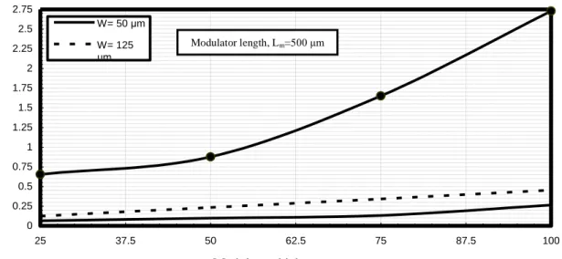
Fig. 13. Variations of modulator power length product against variations of modulator thickness and width at the assumed set of the operating parameters.
0 0.25 0.5 0.75 1 1.25 1.5 1.75 2 2.25 2.5 2.75
25 37.5 50 62.5 75 87.5 100
W= 50 μm W= 125 μm W= 200 μm
Modulator thickness, t, nm
Fig. 14. Variations of modulator power length product against variations of modulator thickness and width at the assumed set of the operating parameters.
M
od
ul
at
o
r
sw
it
chi
ng
spe
ed
,
S
S
,
G
H
z Modulator length, Lm=500 μm
M
o
d
u
la
to
r
p
o
w
e
r
le
n
g
th
p
ro
d
u
c
t,
P
L
P
,
W
a
tt
,
μm Modulator length, L
m=100 μm
M
o
d
u
la
to
r
p
o
w
e
r
le
n
g
th
p
ro
d
u
c
t,
P
L
P
,
W
a
tt
,
μm
639
www.ijarcsee.org
25 50 75 100 125 150 175 200 225 250
1300 1350 1400 1450 1500 1550
VB=0 Volt VB=1.5 Volt VB=3.5 Volt VB=5 Volt
Operating optical signal wavelength, λ, μm
Fig. 15. Optimum modulator length relation to applied bias voltage and operating optical signal wavelength at the assumed set of the operating parameters.
5 10 15 20 25 30 35 40 45 50 55 60 65 70
100 150 200 250 300 350 400 450 500
λ= 1300 nm λ= 1550 nm
Modulator length, Lm, μm
Fig. 16. Modulator phase shift in relation to modulator length and operating optical signal wavelength at the assumed set of the operating parameters.
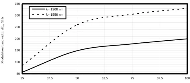
50 100 150 200 250 300 350
25 37.5 50 62.5 75 87.5 100
λ= 1300 nm λ= 1550 nm
Modulator thickness, t, nm
Fig. 17. Modulation bandwidth in relation to modulator thickness and operating optical signal wavelength at the assumed set of the operating parameters.
O
p
ti
m
u
m
m
o
d
u
la
to
r
le
n
g
th
,
LO
p
t.
,
μm
M
o
d
u
la
to
r
P
h
a
se
s
h
if
t,
Δ
φ,
d
eg
re
e
M
od
ul
at
io
n
ba
nd
w
id
th
, Δ
fm
,
G
H
640
www.ijarcsee.org
0 0.5 1 1.5 2 2.5 3 3.5 4 4.5
300 325 350 375 400
λ= 1300 nm λ= 1550 nm
Ambient temperature, T, K
Fig. 18. Modulator temperature coefficient rise in relation ambient temperature and operating optical signal wavelength at the assumed set of the operating parameters.
viii)Figs. (11-14) have proved that modulator switching speed and power length product increases with increasing both width and thickness while decreasing of modulator length.
ix) Fig 15 has assured that modulator optimum length increases with increasing operating optical signal wavelength and decreasing applied bias voltage. x)Fig 16 has indicated that modulator phase shift
increases with decreasing operating optical signal wavelength and increasing modulator length. xi) Fig 17 has assured that modulation bandwidth
increases with increasing both operating optical signal wavelength and modulator thickness.
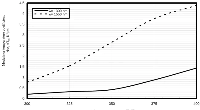
xii) Fig 18 has assured that modulator temperature coefficient rise increases with increasing both operating optical signal wavelength and ambient temperature.
IV. Conclusions
In a summary, the model has been investigated based on GaAs Electro-optic absorption modulator for fast switching speed and high transmission efficiency over wide range of the affecting parameters. It is theoretically found that the increased modulator thickness and operating optical signal wavelength, this results in the increased modulation bandwidth. As well as it is observed that the increased both modulator dimensions (modulator thickness x modulator width), this leads to the increased modulator switching speed and reduced transit time and then to increase power length product through the device. Finally it is theoretically found that the dramatic effects of modulator length and increasing ambient temperatures on the modulator transmission performance efficiency and operation characteristics.
REFERENCES
[1] Abd El-Naser A. Mohammed, Ahmed Nabih Zaki Rashed, and Mohammed S. F. Tabour “Transmission Characteristics of Radio over Fiber (ROF) Millimeter Wave Systems in Local Area Optical Communication Networks,” International Journal of Advanced Networks and Applications, Vol. 2, No. 6, pp. 876-886, 2011.
[2] R. Lew´en, S. Irmscher, and U. Eriksson, “Microwave CAD circuit modeling of a traveling-wave electroabsorption modulator,” IEEE Trans. Microwave Theory Tech., vol. 51, no. 4, pp. 1117–1127, 2003. [3] B. Stegmueller, E. Baur, and M. Kicherer, “1.55 μm and
1.3 μm DFB lasers integrated with electroabsorption modulators for high-speed transmission systems,” in Proc. Second Joint Symposium on Opto- and Microelectronic Devices and Circuits, SODC 2002, pp. 95–99. Stuttgart, Germany, March 2002.
[4] Abd El–Naser A. Mohamed, Ahmed Nabih Zaki Rashed, Sakr A. S. Hanafy, and Amira I. M. Bendary “Electrooptic Polymer Modulators Performance Improvement With Pulse Code Modulation Scheme in Modern Optical Communication Networks,” International Journal of Computer Science and Telecommunications (IJCST), Vol. 2, No. 6, pp. 30-39, Sep. 2011.
[5] R. Lew´en, S. Irmscher, U. Westergren, L. Thyl´en, and U. Eriksson, “Ultra high speed segmented traveling-wave electroabsorption modulators,” in Proc. Optical Fiber Communications Conf., OFC 2003, Postdeadline paper PD38. Atlanta, GA, USA, February 2003. [6] H. Kawanishi, Y. Yamauchi, N. Mineo, Y. Shibuya, H.
Murai, K. Yamada, and H. Wada, “EAM-integrated DFB laser modules with more than 40-GHz
M
o
d
u
la
to
r
te
m
p
e
ra
tu
re
c
o
e
ffi
c
ie
n
t
ri
se
, Δ
Tm
, K
/μ
641
www.ijarcsee.org
bandwidth,” IEEE Photon. Technol. Lett., vol. 13, no. 9, pp. 954–956, 2001.
[7] M. Shirai, H. Arimoto, K. Watanabe, A. Taike, K. Shinoda, J. Shimizu, H. Sato, T. Ido, T. Tsuchia, M. Aoki, S. Tsuji, N. Sasada, S. Tada, and M. Okayasu, “40 Gbit/s electroabsorption modulators with impedance-controlled electrodes,” Electron. Lett., vol. 39, no. 9, pp. 733–735, 2003.
[8] Abd Naser A. Mohammed, Mohamed M. E. El-Halawany, Ahmed Nabih Zaki Rashed, and Sakr Hanafy “High Performance of Plastic Optical Fibers within Conventional Amplification Technique in Advanced Local Area Optical Communication Networks,” International Journal of Multidisciplinary Sciences and Engineering (IJMSE), Vol. 2, No. 2, pp. 34-42, 2011.
[9] T. Kawanishi, T. Sakamoto, and M. Izutsu, “High Speed Control of Lightwave Amplitude, Phase, and Frequency by use of Electrooptic Effect,” IEEE Journal of Selected Topics in Quantum Electronics, Vol. 13, No. 1, pp. 79– 91, 2007.
[10] H. V. Pham, H. Murata, and Y. Okamura, “Travelling Wave Electrooptic Modulators With Arbitrary Frequency Response Utilising Non Periodic Polarization Reversal,” Electronics Letters, Vol. 43, No. 24, pp. 1379–1381, 2007.
[11] Abd El-Naser A. Mohammed, Mohamed Metwae'e, Ahmed Nabih Zaki Rashed, and Amira I. M. Bendary “Recent Progress of LiNbO3 Based Electrooptic Modulators with Non Return to Zero (NRZ) Coding in High Speed Photonic Networks,” International Journal of Multidisciplinary Sciences and Engineering (IJMSE), Vol. 2, No. 4, pp. 13-21, July 2011.
[12] B. Stegmueller, E. Baur, and M. Kicherer, “15GHz modulation performance of integrated DFB laser diode EA modulator with identical multiple quantum well-double stack active layer,” IEEE Photon. Technol. Lett., vol. 14, no. 12, pp. 1647–1649, 2002.
[13] B. Stegmueller and C. Hanke, “High-frequency properties of 1.3 μm and 1.55 μm electro-absorption modulators integrated with DFB lasers based on identical MQW double stack active layer,” in Proc. Lasers and Electro-Optics Society Ann. Meet., LEOS 2002, vol. 1, pp. 115–116. Glasgow, Scotland, UK, November 2002.
[14] M. Peschke, T. Knoedl, and B. Stegmueller, “Simulation and design of an active MQW layer with high static gain and absorption modulation,” in Proc. Numerical Simulation of Semiconductor Devices, NUSOD 2003, pp. 15–16. Tokyo, Japan, October 2003. [15] Ahmed Nabih Zaki Rashed, “New Trends of Forward Fiber Raman Amplification for Dense Wavelength Division Multiplexing (DWDM) Photonic Communication Networks,” International Journal on Technical and Physical Problems of Engineering (IJTPE), Vol. 3, No. 2, pp. 30-39, June 2011.
[16] Abd Naser A. Mohammed, Mohamed M. E. El-Halawany, Ahmed Nabih Zaki Rashed, and Mohammed S. F. Tabour “High Transmission Performance of Radio over Fiber Systems over Traditional Optical Fiber Communication Systems Using Different Coding Formats for Long Haul Applications,” International Journal of Advances in Engineering & Technology (IJAET), Vol. 1, No. 3, pp. 180-196, July 2011. [17] M. Ghanbarisabagh, M. Y. Alias and H. A.
Abdul-Rashid, “Cyclic Prefix Reduction for 20.48 Gb/s Direct Detection Optical OFDM Transmission over 2560 km of SSMF,” International Journal of Communication Systems, Vol. 24, No. 11, pp. 1407-1417, 2011.
[18] A. Kozanecka , D. Szmigifel, K. Switkowski, E. Schabbalcerzak, M. Siwy, “Electro Optic Activity of an Azopolymer Achieved Via Poling With the Aid of Silicon Nitride Insulating Layer,” Optica Applicata, Vol. 41, No. 3, pp. 777-785, 2011.
[19] P. Gerlach, M. Peschke, and R. Michalzik, “High-frequency performance optimization
of DFB laser integrated electroabsorption modulators,” in Proc. Semiconductor and Integrated Opto-Electronics Conference, SIOE 2004, paper 41. Cardiff, Wales, UK, April 2004.
[20] T. Ido, H. Sano, S. Tanaka, and H. Inoue, “Frequency-domain measurement of carrier escape times in MQW electroabsorption optical modulators,” IEEE Photon. Technol. Lett., vol. 7, no. 12, pp. 1421–1423, 1995. [21] B. Stegmueller and C. Hanke, “Integrated 1.3 μm DFB
laser electroabsorption modulator based on identical MWQ double-stack active layer with 25GHz modulation performance,” IEEE Photon. Technol. Lett., vol. 15, no. 8, pp. 1029–1031, 2003.
[22] A. V. Krishnamoorthy, R. Ho, X. Zheng, H. Schwetman, J. Lexau, P. Koka, G. Li, I. Shubin, and J. E. Cunningham, “Computer Systems Based on Silicon Photonic Interconnects,” Proc. IEEE, Vol. 97, No. 7, pp. 1337–1361, 2009.
[23] Abd El Naser A. Mohammed, Ahmed Nabih Zaki Rashed, Gaber E. S. M. El-Abyad, and Abd-El-fattah A. Saad “Applications of Conventional and A thermal Arrayed Waveguide Grating (AWG) Module in Active and Passive Optical Networks (PONs),” International Journal of Computer Theory and Engineering (IJCTE), Vol. 1, No. 3, pp. 290-298, 2009.
[24] Ahmed Nabih Zaki Rashed, “High Performance Photonic Devices For Multiplexing/Demultiplexing applications in Multi Band Operating Regions,” Journal of Computational and Theoretical Nanoscience, Vol. 9, No. 4, pp. 522-531, April 2012.
[25] J. Liu, X. Sun, R. Camacho-Aguilera, L. C. Kimerling, and J. Michel, “Ge on Si Laser Operating at Room Temperature,” Opt. Lett., Vol. 35, No. 5, pp. 679–681, 2010.
[26]Q. Xu, B. Schmidt, S. Pradhan, and M. Lipson, "Micrometer-scale silicon electro-optic modulator," Nature, Vol. 435, No. 3, pp. 325-327, 2005.
642
www.ijarcsee.org
Journal of Engineering and Management Research (IJEMR), Vol. 2, No. 2, pp. 14-22, April 2012. [28]W. M. Green et al., "Ultra-compact, low RF power, 10
Gb/s silicon Mach-Zehnder modulator," Opt. Express, Vol. 15, No. 5, pp. 17106-17113, 2007.
[29] Ahmed Nabih Zaki Rashed, “Recent Developments and Signal Processing of Low Driving Voltage and High Modulation Efficiency Electro-absorption Modulators (EAMs),” International Journal of Image, Graphics, and Signal Processing (IJIGSP), Vol. 4, No. 4, pp. 11-18, May 2012.
Author's Profile
Dr. Ahmed Nabih Zaki Rashed was born in Menouf city, Menoufia State, Egypt country in 23 July, 1976. Received the B.Sc., M.Sc., and Ph.D. scientific degrees in the Electronics and Electrical Communications Engineering Department from Faculty of Electronic Engineering, Menoufia University in 1999, 2005, and 2010 respectively. Currently, his job carrier is a scientific lecturer in Electronics and Electrical Communications Engineering Department, Faculty of Electronic Engineering, Menoufia university, Menouf. Postal Menouf city code: 32951, EGYPT.
![Table 1: Parameters for electro-absorption modulators [3, 6, 9, 22].](https://thumb-us.123doks.com/thumbv2/123dok_us/8087848.2142989/2.892.449.831.677.1049/table-parameters-for-electro-absorption-modulators.webp)