International Journal of Advanced Research in Computer Science and Electronics Engineering (IJARCSEE) Volume 1, Issue 8, October 2011
7
All Rights Reserved © 2012 IJARCSEE
Development of Optical Interconnections Modules
System Architectures and Its Backplane
Technology for Terabit Systems
Dr. Ahmed Nabih Zaki RashedI. Electronics and Electrical Communications Engineering Department Faculty of Electronic Engineering, Menouf 32951, Menoufia University, EGYPT
Abstract- This paper has proposed the new progress of optical interconnections is processed, taking into account the following items such as its ultimate device bandwidth, its available transmission bit rates based on either soliton or maximum time division multiplexing (MTDM) transmission techniques, its ultimate transmission link bandwidth, and the product of the link bandwidth and its transmission length. Two items of special emphasis in the basic design of optical interconnection are: aluminum gallium arsenide (AlGaAs) and Barium Fluoride (BaF2) waveguides, and the optical source cast as Vertical Cavity Surface Emitting Laser Diodes (VCSELD), made of either AlGaAs at operating wavelength of 0.85 µm or indium gallium arsenide phosphors (InGaAsP) at operating wavelength of 0.65 µm, special emphasis is focused on the both above two items under different operating conditions including both the thermal and electrical effects. The optical interconnect is built up on the bases of two VCSELD and one optical link where thermal effects of both diodes and links are included. The good performance of the optical interconnect is deeply and parametrically investigated under wide ranges of the affecting parameters. The high speed performance is processed through three different effects, namely the device 3-dB bandwidth, and the link dispersion characteristics.
Index terms- Optical Interconnect, BaF2, AlGaAs, InGaAsP, Computing Networks, and Optical link.
I.INTRODUCTION
The main problems facing the development of the optical computer is related to one of its main benefits. Because photons do not interact with each other like electrons, it is still necessary to include transistors that perform a switch on or off on the signal. Until researchers can develop an optical switch that will perform the same functions as a transistor, the development of optical computer will remain a thing of the future [1]. The optical interconnects field has experienced a continuous push into applications with ever-shorter transport path lengths [2]. This drive started only a brief time after the widespread deployed of long-haul optical fiber began about 30 years ago, and has been accelerating ever since. Significant optical interconnect research and development activities now span a length-scale of about seven order of magnitude, ranging from dense wavelength division multiplexing (DWDM) based long-haul transport, routing, and switching-for signal transport in the hundreds of kilometers range [3]. In recent years, a new type of semiconductor laser has attracted considerable interest, namely, the vertical cavity surface emitting laser (VCSEL). This device offers many advantages over edge-emitters, resulting in its growing popularity in the field of optoelectronics, including single-longitudinal-mode operation, circular output beams,
suitability for monolithic two dimensional integration, and compatibility with on-wafer probe testing [4]. The architecture of VCSEL can make particularly good use of the broad quantum-well gain bandwidth for the generation of ultra short pulses, and can easily achieve gigahertz-level repetion rates. Although VCSELs have chiefly attracted interest to date as frequency doubled blue sources, their potential as practical and inexpensive ultra short pulse sources is equally great. It is recently demonstrated a picoseconds mode locked VCSELs operating at 1.5 µrn [5], Most characteristics of GaAs based VCSELs in the 0.8 to 1.0 µm wavelength range are now comparable to those of edge-emitters in the lower power (~1 mW) regime where many short haul data communications applications fall. For these applications, fiber loss and dispersion are generally not significant factors. These VCSELs are also proposed for many applications, ranging from printing to optical switching [6]. Moreover, these lasers have proven power scaling capability, and there are many additional attractive characteristics of VCSELs include their circularly shaped, low numerical aperture output beams for easy coupling to fibers or free space optics; their single-axial mode spectra for potential wavelength division multiplexing (WDM) or wavelength addressing schemes; their high power conversion efficiency in the low power range for reduced heating in highly integrated circuits; and their natural vertical emission or array applications [7]. Optical interconnects provide solutions for almost all the levels in the interconnection hierarchy. The main advantages of optical interconnects are higher density, and higher bandwidth length product. In fact, there exists a break-even length above which optical interconnects are more advantageous than electrical ones in terms of power dissipation and bandwidth. For current technologies, optical interconnects are superior for length > 7 km for a system that has a maximum bit rate of 10 Gbit/sec [8].
Volume 1, Issue 8, October 2011
8
All Rights Reserved © 2012 IJARCSEE II.MODELING DESCRIPTION AND ANALYSIS
II.1.MATERIALS BASED OPTICAL SOURCES
Based on the experimental results in Ref. [9], the following curve fitting for the injection current as a function of bias voltage under the forms :
V
mAI20 1.5 (1)
Where V is the applied voltage in volts, and the output power based on the spirit of [9] can be expressed as:
mWatt I
I I
P00.0350.485 0.0314 0.00224 3, (2) Where I is the injection current in mA and is taken over 7.5 mA, and ∆I = (I-7.5). For simplicity, the threshold current will be assumed to be solely a function of temperature. Also, the modeled offset current using a polynomial function of temperature in the following formulae was cast [10] as:
3 3 2 2 1 0 )
(T a aT aT aT off
I (3)
With temperature, T is in ºC, and Ioff is in mA. Where the coefficients a0-a3 can be determined during parameter extraction. Then for AlGaAs material based VCSELD, the values are a0=3700, a1=1.259x10⁻⁵, a2= 1.259x10⁻⁵, and a3=2.471x10⁹. And for InGaAsP material based VCSELD, the values are a0=6773, a1=1.98x10⁻⁴, a2= 9.377x10⁻⁹, and a3=6.634x10⁸. Based on the assumed basic models of [9, 10], the device bandwidth BW3-dB is an electro-thermal quantity and is cast [9-11] under the following form:
4 3 dB r 1 1 3( o/ r)
BW (4)
With r o20.5B2 (5)
Where BW3-dB is the 3-dB bandwidth, o, and B take their usual definitions as in [9-11] are functions of the thermal dependent on physical parameters and the device offset current Ioff is given by:
Ioff 2.213x1031.179x104T3.355x106T (6) In fact, these quantities are functions of both I0ff, T, and the physical parameters of the devices, also, BW3-dB is a good criterion for the device speed. It is possible to adopt detailed numerical representations of the VCSEL temperature profile as a function of the heat dissipation throughout the device, a much simpler method is to describe the temperature via a thermal rate equation which accounts for the transient temperature increase as a result of heat dissipation [10, 11]. Following this approach, the temperature equation can be written as:
th R P IV T
T 0( 0) (7)
Where Rth is the VCSEL's thermal impedance and T0 is the room temperature, where it assumed that any power not carried in the optical output is dissipated as heat in the device [10], with T0=27 ºC , while Rth0.896 oC/mW.
II.2.MATERIALS BASED OPTICAL LINKS
II.2.1.ALUMINUM GALLIUM ARSENIDE (ALGAAS)
MATERIAL
The set of parameters required to characterize the temperature and operating wavelength dependence of the refractive-index (n), where Sellmeier equation is under the form of [12]:
, 2 4 3 2 2 1 2
A A
A A
n
(8)
The set of parameters is recast and dimensionally adjusted as [12]: A1=10.906, A2=0.975, A3=0.3464499 (T/27), A4=0.002467 (0.93721+2.0857x10⁻⁴ T). Where T is the ambient temperature in ºC. Then the first and second differentiation of Eq. (8) w. r. t λ gives:
, 1 4 2 2 3 2 2 A A
A n d dn (9)
2 ,1 3 2 3 2 2 3 2 2 2 2 A A A n d n d (10)
III.2.2.BARIUM FLUORIDE (BAF2) MATERIAL
The refractive index of this waveguide is cast under the Sellemier equation as the following [13]:
2 6 2 2 5 2 4 2 2 3 2 2 2 2 1 2 1 B B B B B B n (11)
The set of parameters is recast and dimensionally adjusted as:
B1=1.0063, B2=7.5593x10⁻² . (T/T0)2, B3=0.143785, B4=0.132364 . (T/T0)2, B5=3.7885, and B6=46.171. Where T is the temperature of the material in ºC, T0 is the reference temperature and is considered 27 ºC. Then the first and second differentiation of Eq. (11) w. r. t λ gives:
n d dn
2 2
6 2 2 6 5 2 2 4 2 2 4 3 2 2 2 2 2 2 1 . B B B B B B B B B
(12)
4
4
4 ,1 3 2 6 2 2 2 6 2 5 3 2 4 2 2 2 4 2 3 3 2 2 2 2 2 2 2 1 2 2 B B B B B B B B B n d n d
(13)
II.3.NEW TRANSMISSION TECHNIQUES
II.3.1.SOLITON TECHNIQUE
The total bandwidth is based on the total chromatic dispersion coefficient Dt where:
Dt= Dm + Dw (14)
Both Dm, and Dw are given by (for the fundamental mode):
km nm n d n d c
Dm , sec/ .
2 2 (15) km nm n Y n n c n
Dw cladding , sec/ . (16)
Where c is the velocity of the light, 3x10⁸ m/sec, n is the refractive-index of the fiber cable core, Y is a function of wavelength, the relative refractive-index difference Δn is given by the following expression:
,
n n n
n cladding
(17)
International Journal of Advanced Research in Computer Science and Electronics Engineering (IJARCSEE) Volume 1, Issue 8, October 2011
9
All Rights Reserved © 2012 IJARCSEE
,
4 2 02
3 1 t n c A D P NL eff t
(18)
Where nNL is the nonlinear Kerr coefficient, 2.6 x 10⁻²⁰ m2/Watt, Δ is the spectral line width of the optical source in nm, P1 is the peak power in watt, Aeff is the effective area of the cable core fiber in µm2, Dt is the total chromatic dispersion coefficient in nsec/nm.km. Then the pulse intensity width in nsec is given by:
sec , 4 2 1
3 0 n c n P A D t NL eff t
(19)
Then the soliton transmission bit rate per channel is given as the following expression [15]:
channel Gbit
t t
Brsc 0.1, /sec/ 10 1 0 0 (20)
II.3.2.MTDM TECHNIQUE
The maximum bit rates are determined by numerous factors, including the signal modulation rate, the transmission bandwidth through the transmission media, and the response time of the optoelectronic devices. In a communications network, the DWDM system is simply one part of the transmission regime. The pulse broadening of grating-based DWDM imposes inherent limitations on the data transmission bit rates.The total chromatic dispersion in standard single mode fiber that limits the bit rates in system based DWDM communication can be calculated as follows [16]:
M M
n nmkmR
D m d wd
s
t , sec/ .
. (21)
Where Mmd is the material dispersion coefficient in nsec/nm.km, Mwd is the waveguide dispersion coefficient in nsec/nm.km, Δτ is the total pulse broadening due to the effect of total chromatic dispersion, Δ is the spectral linewidth of optical source in nm, and Rs is the link length in km. The material dispersion coefficient is given as:
, 2 2 2 2 2 d n d c d n d c
Mm d s (22)
The waveguide dispersion coefficient is given by the following expression:
V ,F c n n M s cladding wd (23)
Where n2 is the refractive-index of the cladding material, Δn is the relative refractive-index difference, s is the optical signal wavelength, F (V) is a function of V number or
normalized frequency. Based on the work [16], they designed the function F (V) is a function of V as follows:
V 1.38V 6.98V2 13.45V3 4.84V4 1.48V5F (24)
When they are employing V-number in the range of (0 V 1.15) yields the above expression. In our simulation model design, we are taking into account V-number as unity to emphasis single mode operation. Equation (21) can be written in another expression as follows [17]:
sec , .
. R n
Dt s
(25)
Then the MTDM transmission bit rate per optical channel is given by:
channel Gbit
Brm c 0.25, /sec/ 4 1 (26)
For both materials aluminum gallium arsenide, and barium fluoride based optical links, the bandwidth is [18]:
s AlGaAs t AlGaAs R D BW ) ( 44 . 0 (27) s BaF t BaF R D BW ) 2 ( 2 44 . 0 (28)
One item of special interest is the transmission link bit rate within link length product PR where:
Prsc(AlGaAs) = Brsc(AlGaAs) . Rs, Gbit.km/sec (29) Prmc(AlGaAs) = Brmc(AlGaAs) . Rs, Gbit.km/sec (30) Prsc(BaF2) = Brsc(BaF2) . Rs, Gbit.km/sec (31) And Prmc(BaF2) = Brmc(BaF2) . Rs, Gbit.km/sec (32)
III.SIMULATION RESULTS AND DISCUSSIONS
Volume 1, Issue 8, October 2011
10
All Rights Reserved © 2012 IJARCSEE
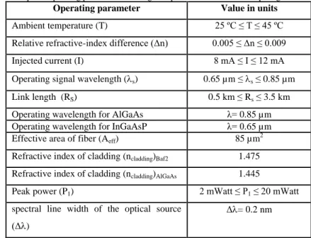
Table 1: Proposed operating parameters for designed optical interconnect in computing data networks.
Operating parameter Value in units
Ambient temperature (T) 25 ºC ≤ T ≤ 45 ºC
Relative refractive-index difference (Δn) 0.005 ≤ Δn ≤ 0.009
Injected current (I) 8 mA ≤ I ≤ 12 mA
Operating signal wavelength (s) 0.65 µm ≤ s ≤ 0.85 µm
Link length (RS) 0.5 km ≤ Rs ≤ 3.5 km
Operating wavelength for AlGaAs λ= 0.85 µm
Operating wavelength for InGaAsP λ= 0.65 µm
Effective area of fiber (Aeff) 85 µm2
Refractive index of cladding (ncladding)Baf2 1.475
Refractive index of cladding (ncladding)AlGaAs 1.445
Peak power (P1) 2 mWatt ≤ P1 ≤ 20 mWatt
spectral line width of the optical source
(Δ)
Δ= 0.2 nm
Based on the set of equations analysis in the modeling basics and description, and the assumed set of operating parameters. The following facts are assured as in clarified in the set of the series of Figs. (1-16):
i) Figs. (1, 2) have demonstrated that as the injected current increases, the device bandwidth also increases for both AlGaAs and In GaAsP materials at constant ambient temperature. As temperature increases, the device bandwidth decreases for both AlGaAs and In GaAsP materials at constant injected current.
ii) As shown in Figs. (3, 4), as both relative refractive-index difference and link length increase, the link bandwidth for both AlGaAs and BaF2 materials decrease.
iii) As in the series of Figs. (5-8), as both relative refractive-index difference and link length increase, the soliton and MTDM bit rates decrease for both AlGaAs and BaF2 based optical link materials. Moreover, the soliton technique present higher bit rate than MTDM technique.
iv) The series of Figs. (9-12) has assured that as both ambient temperature and link length increase, the soliton and MTDM bit rates decrease for both AlGaAs and BaF2 based optical link materials. Moreover, the soliton technique present higher bit rate than MTDM technique.
International Journal of Advanced Research in Computer Science and Electronics Engineering (IJARCSEE) Volume 1, Issue 8, October 2011
11
Volume 1, Issue 8, October 2011
12
International Journal of Advanced Research in Computer Science and Electronics Engineering (IJARCSEE) Volume 1, Issue 8, October 2011
13
Volume 1, Issue 8, October 2011
14
International Journal of Advanced Research in Computer Science and Electronics Engineering (IJARCSEE) Volume 1, Issue 8, October 2011
15
Volume 1, Issue 8, October 2011
16
All Rights Reserved © 2012 IJARCSEE IV.CONCLUSIONS
We have investigated parametrically under the cast of handling the architecture of optical interconnect for high speed optical computing data networks. The design is based on two optical VCSEL diodes of different operating wavelengths s=0.65 µm for InGaAsP based material, and 0.85 µm for AlGaAs based material. Also, the design handles two fiber links made of either aluminum gallium arsenide, or barium fluoride materials. Thus, we have investigated four different designs, where special emphasis and important interest are focused on the following causes and effects shown in Fig. 17.
Fig. 17. Causes and effects in the design of optical interconnect.
The causes are summarized as the following items: the injected current I in mA, the ambient temperature T in ºC, The link length Rs in km, and the relative refractive index difference n. Moreover The effects are summarized as the following items such as the device 3-dB bandwidth in GHz, the links bandwidths, BW(AlGaAs) , BW(BaF2) in GHz, the soliton and MTDM transmitted bit rate, Brsc(AlGaAs), Brsc(BaF2), Brmc(AlGaAs), and Brmc(BaF2) in Gbit/sec. Each optical device has its own thermal and electrical characteristics, also each of the two links has its thermal and spectral characteristics. The increased injection current and the decreased ambient temperature, the largest the device bandwidth. Moreover the decreased of both relative refractive-index difference (Δn), ambient temperature, and link length, the higher of both MTDM and soliton bit rates. Also, the increased link length, and the decreased Δn, the higher of both MTDM and soliton products. AlGaAs based optical source material presents high performance than InGaAsP material, and AlGaAs
based optical link material presents higher transmission bit rates and products than BaF2 material. Thus, the basic architecture of optical interconnect made of VCSELD of AlGaAs at operating wavelength of = 0.85 m with the optical link made of the same material is the best performance architecture.
REFERENCES
[1] N. C. Helman, J. E. Roth, D. P. Bour, H. Altug, and D. A. B. Miller, "Misalignment-Tolerant Surface-Normal Low-Voltage Modulator for Optical Interconnects," IEEE Journal of Selected Topics in Quantum Electronics, Vol. 11, No. 2, pp. 338-342, 2005.
[2] A. Emami-Neyestanak, S. Palermo, H-C. Lee, and M. Horowitz, “CMOS Transceiver With Baud Rate Clock Recovery for Optical Interconnects,” IEEE Symposium on VLSI Circuits, pp. 410-413, June 2004.
[3] A. Krishnamoorthy, X. Zheng, J. Lexau, P. Koka, G. L. Li, I. Shubin, and J. E. Cunningham, "Computer Systems Based on Silicon Photonic Interconnects," Proceedings of the IEEE, Vol. 97, pp. 1337-1361, 2009. [4] I. O'Connor, F. Tissafi-Drissi, J. Dambre, J. Van Campenhout, D. Van Thourhout, J. Van Campenhout, and D. Stroobandt, "Systematic simulation-based predictive synthesis of integrated optical interconnect," IEEE Transactions on Very Large Scale Integration (VlSI) Systems, Vol. 15, pp. 927-940, Aug. 2007. [5] S. K. Selvaraja, P. Jaenen, W. Bogaerts, D. Van
Thourhout, P. Dumon, and R. Baets, "Fabrication of Photonic Wire and Crystal Circuits in Silicon-on-Insulator Using 193-nm Optical Lithography," Journal of Lightwave Technology, Vol. 27, pp. 4076-4083, 2009.
[6] M. Gnan, S. Thoms, R. M. De La Rue, and M. Sorel, "Fabrication of Low Loss Photonic Wires in Silicon-On-Insulator Using Hydrogen Silsesquioxane Electron Beam Resist," Electronics Letters, Vol. 44, pp. 115-116, 2008.
"Low-International Journal of Advanced Research in Computer Science and Electronics Engineering (IJARCSEE) Volume 1, Issue 8, October 2011
17
All Rights Reserved © 2012 IJARCSEE Loss Amorphous Silicon-On Insulator Technology for
Photonic Integrated Circuitry," Optics Communications, vol. 282, pp. 1767-1770, May 2009. [8] L. Vivien, D. Marris-Morini, P. Crozat, J. Damlencourt,
E. Cassan, and S. Laval, "42 GHz PIN Germanium Photodetector Integrated in Silicon-On-Insulator Waveguide," Optics Express, Vol. 17, pp. 6252-6257, 2009.
[9] G. Kim, X. Han, and R.T. Chen, " An 8-Gb/supercomputing Optical Backplane Bus Based on Micro channel Interconnects: Design, Measurements", J. Light wave Technol., Vol. 18, No. 11, pp. 1486, Nov. 2000.
[10] P. V. Mena, J. J. Monkuni, S. M. Kang, A. V. Harton. and K. W. Wyatt, " A Simple Rate-Equation-Based Thermal VCSEL Model", J. Lightwave Technol. Vol. 17, No.5, pp. 865-872. May 1999.
[11] D. Huang, R. Lytel and H. L. Davison, "Optical Interconnects: out of the Box Forever," IEEE J. of Selected Topics in Quantum Electronics, Vol. 9, No. 2, pp. 614-623, March/April 2003.
[12] Osama A. Oraby, “Propagation of An Electromagnetic Beams in Nonlinear Dielectric Slab Wave Guides,” Minufiya Journal of Electronic Engineering Research, Vol. 16, No. 1, pp. 27-44, 2006.
[13] B. Tatian, “Fitting Refractive Index Data With the Sellemier Dispersion Formula,” Applied Optics, Vol. 23, No. 24, pp. 4477-4485, 1984.
[14] D. Agarwal and D. A. B. Miller, “Latency in Short Pulse Based Optical Interconnects,” in 2001 IEEE LEOS Annu. Meeting Conf. Proc., pp. 812–813, 2001. [15] Abd El-Naser A. Mohamed, Abd El-Fattah A. Saad,
Ahmed Nabih Zaki Rashed, and M. Eid “Characteristics of Multi-Pumped Raman Amplifiers in Dense Wavelength Division Multiplexing (DWDM) Optical Access Networks” IJCSNS International Journal of Computer Science and Network Security, Vol. 9, No. 2, pp. 277-284, Jan. 2009.
[16] C. Kroemer, G. Sialm, C. Berger, T. Morf, M. L. Schmatz, F. Ellinger, D. Erni, G.-L. Bona, and H. Jackel, “A 100-mW 4 x 10 Gbit/sec Transceiver in 80-nm CMOS for High Density Optical Interconnects,” IEEE J. Solid-State Circuits, Vol. 40, pp. 2667-2679, 2005.
[17] Y.-C. Chang, C. S. Wang, and L. A. Coldren, “High Efficiency, High Speed VCSELs with 35 Gbit/s Error Free Operation,” Electron. Lett., Vol. 43, pp. 1022-1023, 2007.
[18] G. A. Keeler, B. E. Nelson, D. Agarwal, and D. A. B. Miller, “Skew and Jitter Removal Using Short Optical Pulses for Optical Interconnection,” IEEE Photon. Technol. Lett., Vol. 12, pp. 714–716, June 2000.
Author's Profile
Dr. Ahmed Nabih Zaki Rashed was born in