Art Kay, Timothy Claycomb
TI Designs – Precision: Verified Design
Comparator with Hysteresis Reference Design
TI Designs – Precision Circuit Description
TI Designs – Precision are analog solutions created by TI’s analog experts. Reference Designs offer the theory, component selection, and simulation of useful circuits. Circuit modifications that help to meet alternate design goals are also discussed.
Comparators are used to differentiate between two different signal levels. For example, a comparator may differentiate between an over temperature and normal temperature condition. Noise or signal variation at the comparison threshold will cause multiple transitions. Hysteresis sets an upper and lower threshold to eliminate the multiple transitions caused by noise.
Design Resources
Design Archive All Design files TINA-TI™ SPICE Simulator TLV3201 Product Folder TLV3401 Product Folder TLV1702 Product Folder LMV7291 Product Folder LM397 Product Folder LM331 Product Folder
Ask The Analog Experts WEBENCH® Design Center TI Designs – Precision Library
1
Design Summary
The design requirements are as follows:
Supply Voltage: +5 V
Input: 0V to 5V
The design goals and simulated performance are summarized in Table 1.
Table 1. Comparison of Design Goals, Simulation, and Measured Performance
Goal Simulated Measured (TLV3202) Measured (TLV1702)
VL (Lower Threshold) 2.3V ± 0.1V 2.294V ± 0.001V 2.32V 2.34V
VH (Upper Threshold) 2.7V ± 0.1V 2.706V ± 0.001V 2.74V 2.76V
VH - VL 0.4V± 0.1V 0.412V ± 0.002V 0.42V 0.42V
Total Current (per channel) 100µA 64µA (average) 62.5445uA (average) 539.3uA (average)
Figure 1 depicts the output for a comparator with and without hysteresis with a noisy input triangle waveform applied. The circuit without hysteresis (Vout_no_hyst) has multiple transitions at the threshold voltage whereas the circuit with hysteresis (Vout_hyst) has a single transition at the threshold.
www.ti.com
2
Theory of Operation
Figure 2 shows a typical configuration for a comparator that does not use hysteresis. This configuration uses a voltage divider (Rx and Ry) to set up the threshold voltage. The comparator will compare the input signal (Vin) to the threshold voltage (Vth). The comparator input signal is applied to the inverting input, so the output will have an inverted polarity. When the Vin > Vth the output will drive to the negative supply (GND or logic low in this example). When Vin < Vth the output will drive to the positive supply (Vcc = 5V or logic high in this case). This simple method can be used to determine if a real world signal such as
temperature is above some critical value. However, this method has a shortcoming. Noise on the input signal can cause the input to transition above and below the threshold causing an erratic output.
Figure 2: Comparator without Hysteresis
+
Vin
5V
Vcc
5V
R
x
1
0
0
k
R
y
1
0
0
k
Vout
-+
+VU2 TLV3201
Vth = 2.5V
Vout = GND for Vin > Vth
Vout = V
CC
for Vin < Vth
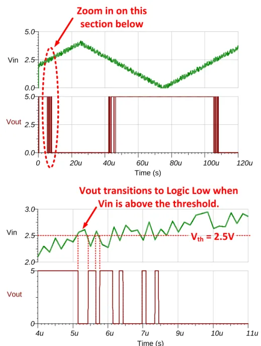
Figure 3 shows the output of a comparator without hysteresis with a noisy input signal. As the input signal approaches the threshold (Vth = 2.5V), it transitions above and below the threshold multiple times. Consequently, the output transitions multiple times. In practical systems, the multiple transitions can create problems. For example, consider the input signal to be temperature and the output to be a critical monitor which is interpreted by a microcontroller. The multiple output transitions do not provide a consistent message to the microcontroller (e.g. whether temperature at a critical level or not).
Furthermore, consider that the comparator output could be used to control a motor or valve. This erratic transitioning near the threshold would cause the valve or motor to be turned on and off multiple times during the critical transition.
Figure 3: Output of a Comparator without Hysteresis showing Multiple Transitions near Threshold Time (s)
0 20u 40u 60u 80u 100u 120u
Vin 0.0 2.5 5.0 Vout 0.0 2.5 5.0
Zoom in on this
section below
Time (s) 4u 5u 6u 7u 9u 10u 11u Vin 2.0 2.5 3.0 Vout 0 5V
th= 2.5V
Vout transitions to Logic Low when
Vin is above the threshold.
www.ti.com
A small change to the comparator circuit can be used to add hysteresis. Hysteresis uses two different threshold voltages to avoid the multiple transitions introduced in the previous circuit. The input signal must exceed the upper threshold (VH) to transition low or below the lower threshold (VL) to transition high. Figure 4 illustrates hysteresis on a comparator. The resistor Rh sets the hysteresis level. When the output is at a logic high (5V), Rh is in parallel with Rx. This drives more current into Ry, raising the threshold voltage (VH) to 2.7V. The input signal will have to drive above VH=2.7V to cause the output to transition to logic low (0V).
When the output is at logic low (0V), Rh is in parallel with Ry. This reduces the current into Ry, reducing the threshold voltage to 2.3V. The input signal will have to drive below VL=2.3V to cause the output to transition to logic high (5V).
Figure 4: Hysteresis Creates Two Thresholds
+ Vin 5V 5V Rh 576k R x 1 0 0 k R y 1 0 0 k Vout_hyst -++V U2 TLV3201
5V
5V R x 1 0 0 k R y 1 0 0 k R h 5 7 6 k 5V2.7V
V
H= 2.7V
+ Vin 5V 5V Rh 576k R x 1 0 0 k R y 1 0 0 k Vout_hyst -++V U2 TLV32010V
5V R x 1 0 0 k R y 1 0 0 k Rh 5 7 6 k2.3V
V
L= 2.3V
Vin > 2.7V causes Vout
to transition to 0V
Vin < 2.3V causes Vout
to transition to 5V
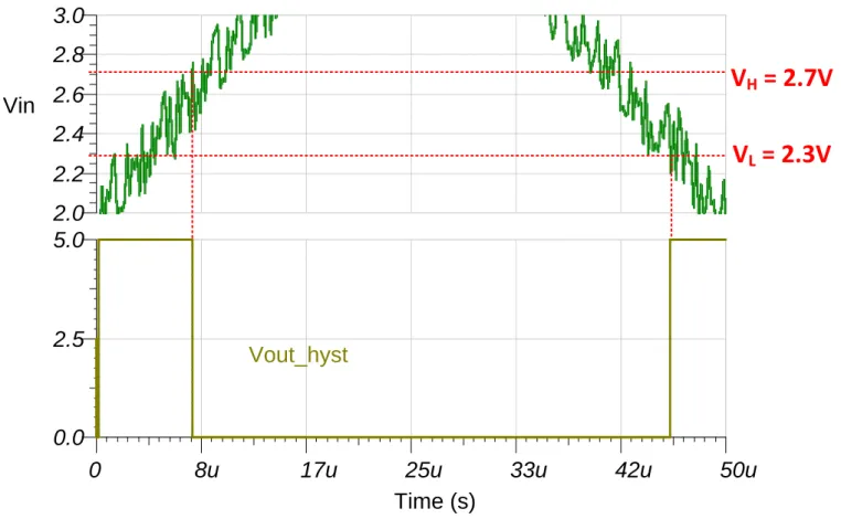
Figure 5 illustrates the output of a comparator with hysteresis with a noisy input signal. The input must transition above the upper threshold (VH = 2.7V) for the output to transition to logic low (0V). The input must also transition below the lower threshold for the output to transition to logic high (5V). The noise in this example is ignored because of the hysteresis. However, if the noise were larger than the hysteresis range (2.7V – 2.3V) it would generate additional transitions. Thus, the hysteresis range must be wide enough to reject the noise in your application. Section 2.1 provides a method for selecting components to set the thresholds according to your application requirements.
Figure 5: Output of a Comparator with Hysteresis Showing Single Transition
Time (s)
0
8u
17u
25u
33u
42u
50u
Vin
2.0
2.2
2.4
2.6
2.8
3.0
Vout_hyst
0.0
2.5
5.0
V
H= 2.7V
V
L= 2.3V
www.ti.com
2.1
Design of Hysteresis Comparator
Equations (1) and (2) can be used to select the resistors needed to set the hysteresis threshold voltages VH and VL. One value (Rx) must be arbitrarily selected. In this example, Rx was set to 100kΩ to minimize
current draw. Rh was calculated to be 575kΩ, so the closest standard value 576kΩ was used. The proof
for Equations (1) and (2) is given in Appendix A.
(1) (2) (3) Let (4) (5) ( ) (6)
3
Component Selection
3.1
Comparator Selection
This method can be used for any comparator. In this example we are optimizing for low power, so the TLV3201 was used because it has la low quiescent current (36µA).
3.2
Passive Component Selection
Standard 0.1% metal film resistors were used in simulations. Section 4.1 shows the accuracy and distribution of the hysteresis thresholds. Other tolerance can be used depending on your accuracy and cost considerations.
www.ti.com
4
Simulation
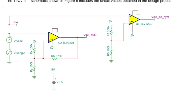
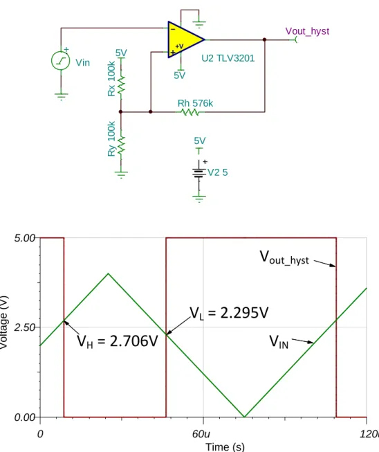
The TINA-TITM schematic shown in Figure 6 includes the circuit values obtained in the design process.
Figure 6: TINA-TITM Schematic
5V 5V 5V 5V 5V Rh 576k R x 1 0 0 k R y 1 0 0 k V2 5 Vout_hyst + Vnoise Vin + Vtriangle R 4 1 0 0 k R 5 1 0 0 k Vout_no_hyst -++V U1 TLV3201 -++V U2 TLV3201
4.1
Hysteresis Thresholds
Figure 7 shows the test of the simulation verifying the threshold voltages on the comparator with hysteresis. The input is an ideal triangle waveform (no noise). Cursers were used post simulation to determine the threshold voltages. The error is primarily from the comparator offset voltage and the difference between the standard resistor value and the ideal value (i.e. Ideal Rh = 575kΩ and Standard Value Rh = 576kΩ).
Figure 7: Simulated Nominal Threshold Values
T Time (s) 0 60u 120u V o lt a g e ( V ) 0.00 2.50 5.00 5V 5V 5V Rh 576k R x 1 0 0 k R y 1 0 0 k V2 5 Vout_hyst + Vin -++V U2 TLV3201
V
L
= 2.295V
V
H
= 2.706V
V
IN
V
out_hyst
www.ti.com
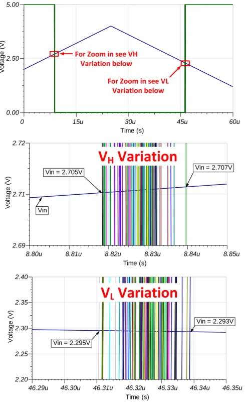
Figure 8 shows the results for a Monte Carlo analysis of the circuit from Figure 7. In this simulation the effect of resistor tolerance (0.1%) on the threshold voltages was determined.
T
Time (s)
0 15u 30u 45u 60u
V o lt a g e ( V ) 0.00 2.50 5.00 T Vin Vin = 2.705V Vin = 2.707V Time (s)
8.80u 8.81u 8.82u 8.83u 8.84u 8.85u
V o lt a g e ( V ) 2.69 2.71 2.72 Vin = 2.707V Vin = 2.705V Vin
For Zoom in see VH Variation below
V
H
Variation
For Zoom in see VL Variation below T Vin = 2.295V Vin = 2.293V V o lt a g e ( V ) 2.30 2.35 2.40 Vin = 2.293V Vin = 2.295V
V
L
Variation
4.2
Current Consumption
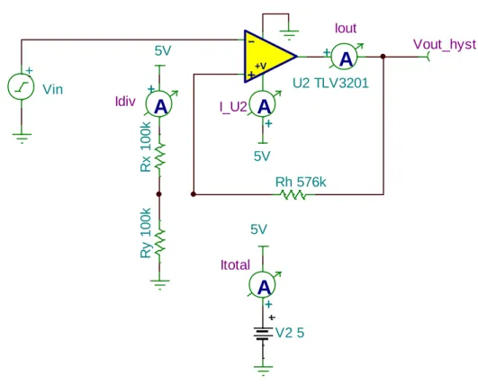
Figure 9 is the simulation test circuit used to confirm current flow in this circuit. This simulation was done because low current consumption is a key design consideration for this example. The voltage divider (Idiv) and the comparator quiescent current (I_U2) are the primary current consumers. The output current (Iout) is minimal because Rh is a large resistance (Rh = 576kΩ).
Figure 9: Circuit for Simulation of Circuit Current Draw
5V 5V 5V Rh 576k R x 1 0 0 k R y 1 0 0 k V2 5 Vout_hyst + Vin -++V U2 TLV3201
A
+ ItotalA
+ I_U2A
+ IoutA
+ Idivwww.ti.com
Figure 10 shows the current draw waveforms for the circuit from Figure 9. The average total current consumption is about 64µA. The current from the divider was simulated to be 23µA and 27µA (calculated = 5V / 200kΩ = 25µA). The divider current could further be reduced by choosing a larger divider
resistance. The quiescent current (I_U2) simulates as 39µA (36µA from the data sheet). Note that the device draws significant transient current when the output transitions state. For this reason current
consumption will increase during high speed output switching. It is also important to properly decouple the comparator so that the transient current is provided by the decoupling capacitor. Use a 0.1µF ceramic X7R capacitor connected closely to the power supply and ground connection.
T I_U2 = 39uA Idiv = 27uA Idiv = 23uA Itotal = 62uA Itotal = 66uA
Time (s)
0
60u
120u
I_U2
0
100u
200u
Idiv
0
50u
Iout
-5u
5u
Itotal
0
100u
200u
Vin
0
2
4
Vout_hyst
0.0
2.5
5.0
Idiv = 23uA Idiv = 27uAItotal = 66uA Itotal = 62uA I_U2 = 39uA
4.3
Simulated Results Summary
Table 2 summarizes the simulated performance of the design.
Table 2. Comparison of Design Goals and Simulated Performance
Goal Simulated
VL (Lower Threshold) 2.3V ± 0.1V 2.294V ± 0.001V VH (Lower Threshold) 2.7V ± 0.1V 2.706V ± 0.001V
VH - VL 0.4V± 0.1V 0.412V ± 0.002V
www.ti.com
5
PCB Design
The PCB schematic and bill of materials can be found in the Appendix B.
5.1
PCB Layout
The PCB shown in Figure 11 is composed of two layers with all power traces and most signal traces routed on the top layer. The remainder of the top layer is poured with a solid ground plane. Minimal signal traces were routed on the bottom layer to ensure a low impedance path for any return currents on the bottom layer ground plane. Vias were placed at each components ground connection to route return currents to the bottom plane and provide the shortest possible path back to ground. General guidelines for PCB layout were followed. For example, input signal trace lengths were kept to a minimum and decoupling capacitors were placed close to the power pins of the device. This PCB can be used for different types of comparators, such as push-pull, open collector, and open drain. If a pull up resistor is not needed, resistors R1, R2, and R3 can be removed without effecting performance.
6
Verification & Measured Performance
6.1
Functional Verifications
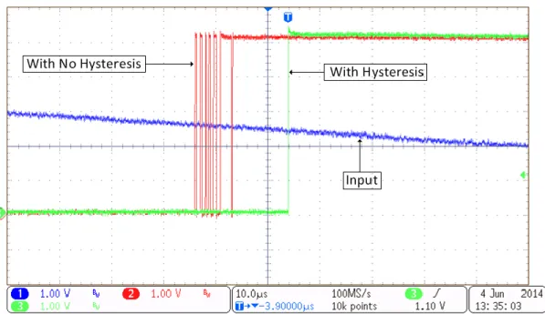
Figure 12-13 shows the input signal (blue), the rising edge output with no hysteresis (red) and the rising edge output with hysteresis (green) of theTLV3202 and TLV1702, respectively. With no hysteresis, there are multiple transitions at the comparison threshold due to noise on the input signal. These transitions may be the input to a microcontroller, which would not provide a consistent signal for the microcontroller to interpret. Hysteresis gives one clean transition at the upper and lower threshold, which provides a consistent signal to the microcontroller.
www.ti.com
6.2
Measurements
Figure 14 shows a threshold level of 2.5V for the output with no hysteresis. An input signal (blue) of 5Vpp
and a 2.5V offset was used to take this measurement. To prevent multiple transitions at the threshold level, an input signal with minimal noise was used.
Input
Output
2.5V
2.5V
Figure 14: Threshold level with no hysteresis
Measurements of the upper threshold (VH) and lower threshold (VL) of the TLV3202 and TLV1702 output with hysteresis are shown in Figures 15-16.
2.74V
2.76V
2.34V
Input
Output
Figure 16: TLV1702 upper and lower threshold with hysteresis
Table 3: Comparison of Calculated and Measured Performance
Calculated Measured (TLV3202) Measured (TLV1702)
VL (Lower Threshold) 2.3V 2.32V 2.34V
VH (Upper Threshold) 2.7V 2.74V 2.76V
VH - VL 0.4V 0.42V 0.42V
While the calculated threshold limits were 2.7V and 2.3V, there are multiple factors that can effect this measurement, such as, passive element tolerances or a pull-up resistor at the output.
www.ti.com
7
Modifications
The hysteresis circuit can be used for any comparator. Table 4 provides examples of different comparators that can be used to achieve different design objectives.
Table 4. Recommended Comparators
Output Amplifier Design Objective Vs Iq µA Vos mV tpd ns tr ns tf ns Approx. Price US$ / 1ku
TLV3201 Micro Power, Low Supply, Wide Bandwidth, Push-Pull
2.7V to 5.5V
36 5 47 4.8 5.2 0.40
TLV3401 Nano Power, Low Supply, Wide Bandwidth, Open-Drain
2.5V to 16V
0.47 0.25 175,000 300,000 5000 0.60
TLV1702 Micro Power, Low Supply, Open Collector
2.2V to 36V
55 3.5 780 2,000 400 0.61
LMV7291 Micro Power, Low Supply, Push-Pull 1.8V
to 5.5V
9 0.3 - 2100 1380 0.35
LM397 General Purpose, Open Collector, Wide Supply
5V to
30V 2 900 940 0.22
LM331 General Purpose, Open Collector, Low Supply
2.7V to 5.5V
70 1.7 - 1000 500 0.26
The methods described in this design TI Precision Design were derived for a push-pull output stage. An open-collector output stage requires a pull-up resistor (Rp). The pull-up will create a voltage divider at the comparator output that introduces an error when the output is at logic high. This error can be minimized if Rh > 100Rp. Figure 17 shows the design modified for use with an open-collector output. The value of Rp was selected to minimize error (Rh > 100Rp). The output will need to drive 1mA for a logic low (5V/5kΩ = 1mA). Additional increase in all the circuits’ resistance can reduce the output drive requirement if needed.
+
Vin
5V
Vout
-+
+V5V
Rp 5k
8
About the Author
Arthur Kay is an applications engineering manager at TI where he specializes in the support of amplifiers, references, and mixed signal devices. Arthur focuses a good deal on industrial applications such as bridge sensor signal conditioning. Arthur has published a book and an article series on amplifier noise. Arthur received his MSEE from Georgia Institute of Technology, and BSEE from Cleveland State University. Timothy Claycomb joined the Precision Linear Applications team in February 2014. Before joining the team, he was an intern in the summer of 2013. Timothy received his BSEE from Michigan State University.
9
Acknowledgements & References
9.1
Acknowledgements
The author wishes to acknowledge Collin Wells, Tim Green, and Marek Lis for technical contributions to this design.
9.2
References
www.ti.com
Appendix A. Proof for Equation
A.1 Proof of Equation
(1)(7) (8) (9) ( ) ( ) (10)
A.2 Proof of Equation
(2)( ) (11) ( ) (12) ( ) ( ) (13) (14)
Appendix B.
B.1 Electrical Schematic
Figure B-1: Electrical Schematic
B.2 Bill of Materials
IMPORTANT NOTICE FOR TI REFERENCE DESIGNS
Texas Instruments Incorporated ("TI") reference designs are solely intended to assist designers (“Buyers”) who are developing systems that incorporate TI semiconductor products (also referred to herein as “components”). Buyer understands and agrees that Buyer remains responsible for using its independent analysis, evaluation and judgment in designing Buyer’s systems and products.
TI reference designs have been created using standard laboratory conditions and engineering practices.TI has not conducted any testing other than that specifically described in the published documentation for a particular reference design.TI may make corrections, enhancements, improvements and other changes to its reference designs.
Buyers are authorized to use TI reference designs with the TI component(s) identified in each particular reference design and to modify the reference design in the development of their end products. HOWEVER, NO OTHER LICENSE, EXPRESS OR IMPLIED, BY ESTOPPEL OR OTHERWISE TO ANY OTHER TI INTELLECTUAL PROPERTY RIGHT, AND NO LICENSE TO ANY THIRD PARTY TECHNOLOGY OR INTELLECTUAL PROPERTY RIGHT, IS GRANTED HEREIN, including but not limited to any patent right, copyright, mask work right, or other intellectual property right relating to any combination, machine, or process in which TI components or services are used. Information published by TI regarding third-party products or services does not constitute a license to use such products or services, or a warranty or endorsement thereof. Use of such information may require a license from a third party under the patents or other intellectual property of the third party, or a license from TI under the patents or other intellectual property of TI.
TI REFERENCE DESIGNS ARE PROVIDED "AS IS". TI MAKES NO WARRANTIES OR REPRESENTATIONS WITH REGARD TO THE REFERENCE DESIGNS OR USE OF THE REFERENCE DESIGNS, EXPRESS, IMPLIED OR STATUTORY, INCLUDING ACCURACY OR COMPLETENESS. TI DISCLAIMS ANY WARRANTY OF TITLE AND ANY IMPLIED WARRANTIES OF MERCHANTABILITY, FITNESS FOR A PARTICULAR PURPOSE, QUIET ENJOYMENT, QUIET POSSESSION, AND NON-INFRINGEMENT OF ANY THIRD PARTY INTELLECTUAL PROPERTY RIGHTS WITH REGARD TO TI REFERENCE DESIGNS OR USE THEREOF. TI SHALL NOT BE LIABLE FOR AND SHALL NOT DEFEND OR INDEMNIFY BUYERS AGAINST ANY THIRD PARTY INFRINGEMENT CLAIM THAT RELATES TO OR IS BASED ON A COMBINATION OF COMPONENTS PROVIDED IN A TI REFERENCE DESIGN. IN NO EVENT SHALL TI BE LIABLE FOR ANY ACTUAL, SPECIAL, INCIDENTAL, CONSEQUENTIAL OR INDIRECT DAMAGES, HOWEVER CAUSED, ON ANY THEORY OF LIABILITY AND WHETHER OR NOT TI HAS BEEN ADVISED OF THE POSSIBILITY OF SUCH DAMAGES, ARISING IN ANY WAY OUT OF TI REFERENCE DESIGNS OR BUYER’S USE OF TI REFERENCE DESIGNS.
TI reserves the right to make corrections, enhancements, improvements and other changes to its semiconductor products and services per JESD46, latest issue, and to discontinue any product or service per JESD48, latest issue. Buyers should obtain the latest relevant information before placing orders and should verify that such information is current and complete. All semiconductor products are sold subject to TI’s terms and conditions of sale supplied at the time of order acknowledgment.
TI warrants performance of its components to the specifications applicable at the time of sale, in accordance with the warranty in TI’s terms and conditions of sale of semiconductor products. Testing and other quality control techniques for TI components are used to the extent TI deems necessary to support this warranty. Except where mandated by applicable law, testing of all parameters of each component is not necessarily performed.
TI assumes no liability for applications assistance or the design of Buyers’ products. Buyers are responsible for their products and applications using TI components. To minimize the risks associated with Buyers’ products and applications, Buyers should provide adequate design and operating safeguards.
Reproduction of significant portions of TI information in TI data books, data sheets or reference designs is permissible only if reproduction is without alteration and is accompanied by all associated warranties, conditions, limitations, and notices. TI is not responsible or liable for such altered documentation. Information of third parties may be subject to additional restrictions.
Buyer acknowledges and agrees that it is solely responsible for compliance with all legal, regulatory and safety-related requirements concerning its products, and any use of TI components in its applications, notwithstanding any applications-related information or support that may be provided by TI. Buyer represents and agrees that it has all the necessary expertise to create and implement safeguards that anticipate dangerous failures, monitor failures and their consequences, lessen the likelihood of dangerous failures and take appropriate remedial actions. Buyer will fully indemnify TI and its representatives against any damages arising out of the use of any TI components in Buyer’s safety-critical applications.
In some cases, TI components may be promoted specifically to facilitate safety-related applications. With such components, TI’s goal is to help enable customers to design and create their own end-product solutions that meet applicable functional safety standards and requirements. Nonetheless, such components are subject to these terms.
No TI components are authorized for use in FDA Class III (or similar life-critical medical equipment) unless authorized officers of the parties have executed an agreement specifically governing such use.