Copyright © 2012 IJECCE, All right reserved
Development of Data Acquisition System using VLSI
Sonia Dixit
M. Tech. Student, Suresh Gyan Vihar University, Jaipur, Rajasthan
Rekha Agrawal
Asst. Prof., Suresh Gyan Vihar University, Jaipur, Rajasthan
Abstract – Development of Data Acquisition System using VLSI is basically designed to keep the track of the temperature data entering the system, process it and display it on a PC. This VLSI-based Data Acquisition System works as a data logger for measuring the temperature data at different conditions. UART module is used as communication interface between CPLD kit and PC. In this paper, we designed the hardware part as we ll as software implementation part of our system to measure the temperature with the help of temperature sensors and the result is stored in Personal Computer for post process analysis. First the input temperature is detected in analog form and then converted to digital form using analog-digital convertor and then through level convertor it is implemented on CPLD kit. On CPLD kit, VHDL coding is done in Xilinx to read the data entered and logic is being implemented to transfer it to PC for display via serial port using UART. The input data will be synthesized on CPLD device and simulation results can be seen on PC.
Keywords –Temperature, Sensor, Analog-Digital Convertor, Level Convertor, Data Acquisition System, Data Logger, VLSI, UART, PC, VHDL, Xilinx, CPLD.
I. INTRODUCTION
With the advancement of technology, the processes are becoming more and more complex. Due to this increase in complexity, for efficient analysis of process the number of parameters required for data acquisition also increases. Data Acquisition is simply the gathering of information about a system or process. It is the process of collecting data in an automated fashion from analog and digital measurement sources such as sensors and devices under test.
Data acquisition begins with the physical phenomenon or physical property to be measured. Examples of this include temperature, light intensity, gas pressure, fluid flow, and force. Regardless of the type of physical property to be measured, the physical state that is to be measured must first be transformed into a unified form that can be sampled by a data acquisition system. The task of performing such transformations falls on devices called sensors. A data acquisition system works as a data logger which is an electronic instrument that can record digital or analog measurements over a period of time [1].
A VLSI based temperature data logger has been developed for measuring temperature at different conditions [2]. The system is designed and developed to measure the temperature with the help of temperature sensors and the result can be stored in memory for post process analysis. Data acquisition hardware is what usually interfaces bet we en the signal and a PC [3]. During the testing, it is verified that there is continuous
and correct acquisition of data. It is also verified that the data is sequentially stored in memory. This verification is done by using a PC display via UART port [10]. The designed system can be tested under different conditions: at room temperatures, at low temperatures, at different temperatures, readings taken over long time. For all these conditions, the system performed accurately.
II. SYSTEM ARCHITECTURE
To design and implement the VLSI based Data Acquisition System for the temperature data as input to the system which is to be analyzed, recorded and monitored for post process analysis; system architecture designed here consists of the following basic parts:
1) Temperature Sensor (DS1621C Digital Thermometer and Thermostat)
2) Analog to Digital Converter
3) VLSI Kit (CPLD Development Kit XILINX
XC9572XL) [13] 4) Level Convertors
5) Personal Computer with serial port
Fig.1. Block diagram of the System Architecture
Temperature Sensor (DS1621C Digital Thermometer
and Thermostat):
Input applied to our system thetemperature analog data through temperature sensor. The DS1621 Digital Thermometer and Thermostat provides 9-bit temperature readings, which indicate the temperature of the device [4].
Copyright © 2012 IJECCE, All right reserved
Analog-to-Digital Convertor:
Generally, measuredcontinuous signals such as voltage or current are analog signals. An analog-to-digital convertor (ADC) converts analog signals to digital signals. . Thus in our system analog signals from the input source are converted to the digital signals using ADC for the further implementation on the VLSI kit. The ADC has a 750-ms conversion time and 8-bit resolution and a single channel operating with a 5-V single power supply. The power consumption is 15 mW.
The DS1631 uses a band-gap temperature sensing architecture in conjunction with a sigma-delta analog to digital converter to provide digital temperature measurements. The band-gap circuit produces a voltage that varies linearly with temperature. This voltage is converted to a digital value by the analog-to-digital converter (ADC). This architecture allows the user to select 8-bit temperature readings in the configuration register.
Level Convertor:
Level convertor is used twice in thesystem. Firstly, we use it just after analog-to-digital convertor and before VLSI kit to interface analog-to-digital convertor with VLSI kit as level convertor manages the voltage level of both the devices.
Fig.3. MAX232 Chip
The MAX232 [5] is an integrated circuit that converts signals from an RS-232 serial port to signals suitable for use in TTL compatible digital logic circuits. The MAX232 is a dual driver/receiver and typically converts the RX, TX, CTS and RTS signals [6].
VLSI Kit:
VLSI kit can be a CPLD (ComplexProgrammable Logic Device) Kit [13] or a FPGA (Field Programmable Gate Array) kit on which VHDL coding is implemented and simulated [14]. It includes software as well as hardware part i.e. software part is implemented on Xilinx Software while hardware part is implemented on CPLD Development BoardXILINX XC9572XL.
Programmable Logic Devices (PLDs) offer wide range of logic capacity, features, speed and voltage characteristics and these devices can be changed at any time to perform any number of functions. CPLDs are great at handling wide and complex gating at blistering speeds. e.g., 5ns which is equivalent to 200MHz. the timing model for CPLD is easy to calculate, so even before design it can calculate the in to output speeds. CPLDs enable ease of design, lo we r development costs, more product revenue for money, and the opportunity to speed your products to market, etc.
Fig.4. VLSI CPLD Kit
Display:
The output of the system is to be displayed onthe personal computer. Personal computers are basically used as the display device which shows the results and also stores the data for further requirement. PCs may use a serial port to interface to devices via RS232. UARTs are commonly used in conjunction with communication standards RS232 [8].
Fig.5. Display Device
III. SYSTEM DESIGN AND IMPLEMENTATION
For the design and development of the system to measure real-time quantity [7], the methodology used involves the software and hardware implementation. The actual implementation of the system involves the following steps:
1) System Definition 2) Circuit Design
3) PCB Design and Fabrication 4) Hardware Modifications 5) Software Design
6) Integration and Final Testing
The complete design is divided into two parts:
A.
Hardware Implementation
System hardware is designed to keep the track of the temperature data. Here, we have designed two PCBs.
On first PCB, components inbuilt include the input source i.e. the temperature sensor with incorporated analog-to-digital convertor along with the level convertors.
Copyright © 2012 IJECCE, All right reserved Fig.6. Designed System Hardware
B. Software Implementation
Software design includes developing codes for the system, allocating blocks as per functionality, writing the separate modules for UART protocol [10] and different interfacing devices and testing them on the designed hardware. Interfacing of CPLD with ADC, PC, etc. has been carried out using various software modules. The control program is written in VHDL (VHSIC hardware description language) [9]. The software is able to show the real time values from the analog channels for immediate analysis.
Fig.7.Xilinx ISE Simulator
Xilinx ISE is the software simulation tool used for the coding in VHDL [11] which commonly used language to write text models that describe a logic circuit. A simulation program is used to test the logic design using simulation models to represent the logic circuits that interface to the design. Coding simulated in the Xilinx ISE will then be burn on CPLD development board for interfacing it with PC [12].
IV. SIMULATION RESULTS
The designed system is tested and simulated under different conditions: at room temperature, at low temperatures, at high temperatures, readings taken over long time at Baud rate 9600 Display reading as well as simulation result is same for a particular temperature showing the accurate working of the system.
A.
Temperature = 10°C (Low Temperature)
Fig.8. Display of Data Acquisition System Reading on PC at 10°C
Fig.9. Simulation of Temperature Data at 10°C
Copyright © 2012 IJECCE, All right reserved
B.
Temperature = 38°C (Room Temperature)
Fig.10. Display of Data Acquisition System Reading on PC at 38°C
Fig.11. Simulation of Temperature Data at 38°C
Similarly, we show 8-bit data as “00100110” for 38°C (room temp.) detected as din[7:0] pin sending at 9600 Baud Rate to transmitter, so first we have to set Reset=’0’ to read the data by transmitter. Then tx_baud_generator send the data at 9600 Baud Rate to receiver already set at 9600 Baud rate. So Receiver receives the 8-bit data “00100110” as “00100110” using dout[7:0] pin at 9600 baud rate which can be different at different baud rate. This 8-bit data transmit to Automatic Baud Detection Block, where both baudclk are matched and we will receive the same data ”00100110” at rx_out [7:0] and rx_done_tick signal is set to low which Indicates that new data has been received, and is ready to be read out. Received temperature data can be matched with the display reading.
C.
Temperature = 102°C (High Temperature)
Fig.12. Simulation of Temperature Data at 102°C
Fig.13. Display of Data Acquisition System Reading on PC at 102°C
In this, we show 8-bit data as “01100110” for 102°C (high temperature) detected as din[7:0] pin but we want to send this data at 9600 Baud Rate to transmitter so first we have to set Reset=’0’ to read the data by transmitter. Then tx_baud_generator send the data at 9600 Baud Rate to receiver. We have already set the Receiver Baudclk at 9600. So Receiver receives the 8-bit data “01100110” as “01100110” using dout[7:0] pin at 9600 baud rate which can be different at different baud rate. This 8-bit data transmit to Automatic Baud Detection Block, in which both baudclk are matched and we will receive the same data ”01100110” at rx_out[7:0] and rx_done_tick signal is set to low which Indicates that new data has been received, and is ready to be read out.
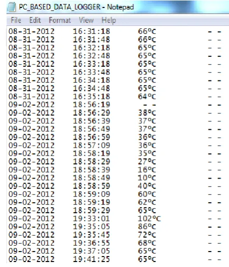
All these logged data can be seen on PC in the tabular form which keeps the record of all temperature data at regular intervals.
Copyright © 2012 IJECCE, All right reserved
V. CONCLUSION
This paper presented the designing and the implementation of Data Acquisition System using VLSI, where we used temperature data as the input.
Previously designed Data Acquisition Systems are basically implemented on microcontrollers only but here in this paper we have implemented on VLSI kit using VHDL coding whose simulation results are discussed above.
Data Acquisition is simply the process of collecting data that measure real world physical conditions and the resulting samples can be visualized and stored on a computer. Data Acquisition System used here monitors and records the varying temperature data in the System. The designed system uses the UART Protocol designed in VHDL and implemented on the Spartan3 device. UART is used for the asynchronous serial data communication bet we en CPLD kit and PC using RS232 Standards. Finally the input data will be synthesized on CPLD device and simulation results can be seen on PC.
These features make the Data Acquisition System a system of choice and a system of future, having unlimited scope for development and expansion.
VI. FUTURE ASPECTS
The Development of Data Acquisition System using VLSI can further be implemented for simultaneous inputs. Here we considered a single input source as temperature sensor, which can further be implemented with multiple inputs, as inputs can be monitored at different serial ports on the PC indicating which input will be on which port. Secondly the single input source an also be implemented with different baud rates as here we considered a baud rate of 9600 only.
System can be programmed to work as a temperature alarm integrated with a notification service through (SMS)/email.
REFERENCES
[1] Andrew J Thompson, John L Bahr and Neil R Thomson, “Low po we r data logger”, proceedings of conference department of
physics, university of Otago, Dunedin.
http/www.loggingtutorial/dr.saulgreenburg/htm.
[2] Peter Roberson, “Using data loggers”, science teachers’ workshop, 2004, northSydney.
[3] Data logger / Recorder / Data Acquisition - Background information Byte Paradigm - explains the differences bet we en data logging and data acquisition
[4] http://en.wikipedia.org/wiki/temperature-measurement
[5] Maxim MAX232 datasheet
(http://datasheets.maxim-ic.com/en/ds/MAX220-MAX249.pdf)
[6] Texas Instruments, Inc. MAX232, MAX232I – Dual EIA-232 Drivers/Receivers, February 1989
[7] P. Pushner and A. Burns. Writing temporally predictable code 7th IEEE International Workshop on object oriented Real Time Dependable systems, San Diego,California , USA, Jan 2002 [8] EIA standard RS-232-C: Interface bet we en Data Terminal
Equipment and Data Communication Equipment Employing Serial Binary Data Interchange. Washington: Electronic Industries Association. Engineering Dept. 1969. OCLC
38637094 (//www.worldcat.org/oclc/38637094).
[9] Yang Jinhong Hong Yongqiang, “Design of UART Based on ARM+DSP Distributed Data Acquisition System” ISBN:-1-4244-1135-1 2007, Eighth International Conference on Electronic Measurement and Instruments.
[10] Universal Asynchronous Receiver/Transmitter, Lattice Semiconductor Corporation, February 2002. http://www.msc-ge.com/download/lattice/files/rd1011.pdf
[11] Mohd Yamani Idna ldris and Mashkuri Yaacob, “A VHDL Implementation of BIST Technique in UART Design” IEEE 2003 , poster paper pages(s):1451-1454,TENCON.
[12] ISE ISim In-Depth Tutorial UG682 (v 12.3) September 21, 2010 http://www.xilinx.com/
[13] Ma, Y., Wang, D.-L., Wang, L.-Y.: CPLD / FPGA programmable logic devices and practical tutorial, pp. 10–12. Mechanical Industry Press, Beijing (2006)
[14] Wang, C., Wu, J.-H., Fan, L.-Z., Xue, N., Xue, X.-G.: Altera FPGA/CPLD Design (Fundamentals), pp. 11–13. People's Posts & Telecom Press, Beijing (2005)
AUTHOR’S PROFILE
Sonia Dixit
was born in Jaipur (Dist.), Rajasthan, India on 7th December, 1986. She received her B. Tech. degree in Electronics & Communication Engineering from Rajasthan College of Engineering for Women (RCEW), Bhankrota, Jaipur, affiliated to the
University of Rajasthan, Jaipur, Rajasthan, India in 2008. She is pursuing M. Tech. in Electronics & Communication Engineering in the field of VLSI Engineering, from Suresh Gyan Vihar University (SGVU), Jagatpura, Jaipur, Rajasthan, India.
She had worked as LECTURER in Department of Electronics & Communication in Baldev Ram Mirdha Institute of Technology (BMIT). Her main research is in the field of VLSI.
She has published 02 Technical papers the reputed International Journals and 07 Technical papers in reputed International and National conferences.
Rekha Agrawal
was born in Agra (Dist.), Uttar Pradesh, India on 14th March, 1988. She received her M. Sc. (Electronics) degree from Banasthali University, Jaipur, Rajasthan, India in 2009 and M. Tech. in Electronics & Communication Engineering in the field of VLSI Design from Banasthali University, Jaipur, Rajasthan, India.
She had worked as TRAINEE in Defence Laboratory, Jodhpur. She is presently working as ASSISTANT PROFESSOR in Department of Electronics & Communication in from Suresh Gyan Vihar University (SGVU), Jagatpura. Her main research is in the field of VLSI.