Design and Implementation of Simultaneous Shield
And Repeater Insertion for On-chip Interconnects
1
M.Surendra Goud
M.Tech (VLSI), KCE Engg College Kurnool, INDIA
2
Mr.Y.Sreenivas Goud
HOD OF ECE DEPT, KCE Engg College Kurnool, INDIA
Abstract
-
A Resource based optimization is a new approach for high performance integrated circuits. The method is applied to simultaneous shield and repeater insertion, resulting in minimum coupling noise under power, delay, and area constraints Repeater insertion is a well known design technique to reduce the delay required to propagate a signal along a line. Shielding inserts an additional line between a victim line and an aggressor line. Finally placing a shield beside and inserting repeaters along a victim line and are chosen to exemplify the resource based optimization process. In the active shielding architecture shield driving circuits as 4:1 multiplexer, full adder, multipliers are inserted. The power consumption of active shielding architecture is observed to be approximately 20% less compare to passive shielding architecture. The main aim of this is minimize the coupling noise under power, delay, and area constraintsKeywords
-
Optimization, power, delay, noise, repeater insertion, resources, shielding.I. I
NTRODUCTIONFurther increases in integrated circuit (IC) scaling requires more efficient devices, circuits, and systems in terms of power, delay, noise, and area. Efficient optimization processes are therefore required. To achieve this capability, many different design techniques are used.
For interconnect, low-swing interconnects [2], cascaded buffers [3], repeater insertion [4], shielding [5], differential signaling [6], [7], active regeneration [8], [9], intentional skewing [10], bus swizzling [11], [12], and tapered interconnects [13] are well known design techniques.
Optimization processes and related design techniques applied to high performance ICs are the topic of this project. A standard optimization process is based on a cost function. There are two steps involved in this process, i.e., building a function and determining the optimal value of the function. The cost function is typically a sum of coefficients multiplied by the resources or a product of resources with power coefficients, such as
Cost=α1.pwer+α2.delay+α3.noise+α4.area……...(1) Cost=powerβ1.delayβ2.noiseβ3.areaβ4………..(2)
Where α and β characterize the importance of a particular resource.
II. Resource based Optimization Process
Limitations in standard optimization processes are described in Section II-A. The theory and limitations of resource based optimization processes are presented in section II-B and II-C.
A. Limitations in Standard Optimization Processes
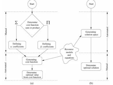
A general flow for a standard optimization process is shown in Fig. 1(a). The primary disadvantage of this flow is the need for user involvement before the optimization process is initiated.
Fig (1): Optimization flow diagram (a): standard, (b) resource based optimization
The cost function and coefficients must be allocated for each resource. For the same system, two users may choose different coefficients and thereby produce different results. Additionally, some resources have changing importance. These aspects constrain the standard optimization process.
B.Resource Based Optmization Process
To overcome these limitations, a different resource based optimization process is proposed. The user involvement occurs at the end of this process. In Fig. 1(b), a flow diagram of this resource based optimization process is presented. In order to provide insight into the resource based optimization flow, consider a system where
Area = f1 (width)…. (3) Noise = f2 (width).... (4)
A fundamental assumption in (3) and (4) is that the width determines the area and noise. Conversely, the area or noise may determine the width. By inverting (3), the same system is described by
Width=fi־¹ (area)…………... (5)
Substituting (5) into (6), the same system can be characterized by
Noise=f2 [f1־¹ (area)]... (7)
This system representation describes the relationship between the two resources and can be presented as a tradeoff line.
Power, area, noise, and delay are four primary design criteria. The number of variables, e.g., line width, shield width, number of repeaters, and power supply, is typically high. Any system can be represented by n variables n+1and resources.
Res1=f1 (α1,α2,α3……….…….αn) Res2=f2 (α1,α2,α3…….……….αn)
C. Limitations in Resource Based Optimization Processes: Resource based optimization also exhibits limitations. These limitations can be categorized as follows:
1) Model inaccuracies. 2) Function inversability.
In a standard optimization process, inaccuracy in the models produces quantization error. In resource based optimization, however, this error is cumulative. Due to these additive errors, the models used in this optimization process must be sufficiently accurate. Otherwise, only the fidelity of the final function may be useful.
Function inversability is a different limitation in resource based optimization processes. For y=f(x), where x cannot be directly extracted, certain techniques are required to provide inversability. Some of these techniques are truncation, Taylor expansion, and approximation, which can lead to greater model inaccuracy.
Any design constraint may be characterized as a resource. Some constraints, such as power and area, are more commonly treated as a resource. Other design objectives, such as delay or noise, are less commonly referred to as a resource.
A practical application is composed of a combination of optimization processes and multiple design techniques. A methodology that considers these issues in an integrated fashion is the focus of this project. Two different techniques that provide immunity to coupled noise, namely, shield and repeater insertion, have been combined based on resource optimization to exemplify this process. Each of the techniques exhibits different power, delay, noise, and area resource characteristics.
III. S
HIELD ANDR
EPEATERI
NSERTIONA. Shielding
Shielding inserts an additional line between a victim line and an aggressor line. This technique can be divided
into two major categories: passive and active
shielding.
Fig. (2): Interconnect structure consisting of two shielded signal lines
Fig. (3): Passive Shielding
A well-known technique to reduce coupling effects is to insert static (ground or power) lines between bus data lines, as shown in Fig (3). This technique is known as passive shielding. Passive shielding eliminates the worst-case switching condition when two adjacent lines oppositely switch, resulting in a better worst-case delay.
B. Repeater Insertion
Repeater insertion is a well known design technique to reduce the delay required to propagate a signal along a line [4]. A method of inserting repeaters into a complex integrated circuit includes the step of selecting, based upon signal transition data, a maximum wire length to be positioned between two repeaters in a complex integrated circuit. It is impractical, however, to insert excessive repeaters due to delay, power, and area constraints.
Fig. (4): Wire sizing in a repeater insertion system
C. Simultaneous shield and repeater insertion
Four primary resources for simultaneous shield and repeater insertion are considered: power, delay, noise, and area. In this project, the resource models are based on a 0.18 m CMOS technology.
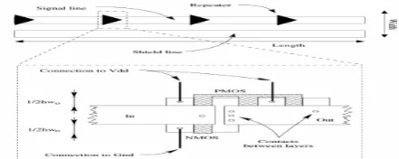
Fig. (5): Schematic layout of a signal line with shield line and repeaters to reduce coupling noise.
IV. A
CTIVES
HIELDINGThe conventional fully shielded bus architecture, in which a shield is inserted between each adjacent pair of lines, was originally proposed to reduce both the noise coupling between lines and theline’s worst-case delay by reducing the worst case MCF of any line from 4.0 to 2.0. However, shielding doubles the area of the bus. Another intermediate shielding solution, the half-shielded bus, is also used and trades-in some of the shielding advantages to gain more area by inserting a shield after every two bus lines instead of after each line. Compared to the fully shielded bus, this bus architecture has 25% less area, but the worst case MCF of any line is 50% higher (3.0 instead of 2.0). Thus, this half shielded bus architecture will have either a higher delay or larger repeaters and energy dissipation for the same delay of a conventional fully shielded bus.
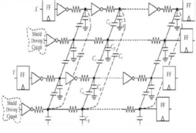
Fig. (6): Active Shielding Circuit
A. 2-Bit Shielding
Compared to passive shielding, active shielding reduces the MCF of some of the switching cases by allowing the shield to switch. Although this reduces the energy dissipation due to coupling, it increases the energy dissipation of self-switching due to the switching of the shield. Thus, the effectiveness of active shielding as compared to passive shielding will depend on the relative value of the reduction in coupling energy dissipation compared to the self-switching energy dissipation.
Transistor sizes in flip-flops and repeaters are optimized using the HSPICE global optimizer and circuit simulator. For a given bus length (flop-to-flop distance), the optimizer selects the optimal segment length (distance between two consecutive repeaters) to minimize the total energy of the bus while meeting a target cycle time requirement of 500 ps as given by:
Tbus = TCQ + Tline + Tshield + Tsetup + Tskitter≤500 ps
Where TCQ is the clock-to-out delay of the driver FF, Tline is the line delay, Tshield is the propagation delay of the shield encoding circuit (f) for the active shield lines, Tsetup is the setup time at the receiver flop, and Tskitter is a fixed quantity that accounts for clock skew and jitter between the driver and the receiver flops.
Fig. (7): 2-Bit Shielding.
B. 4-BIT UN Shielding Circuit
The 4-bit UN shielding circuit diagram is shown in fig (8). In the UN shielding circuit there is no shield lines are place only repeaters are inserted. So in the above circuit coupling capacitors are not grounded. So compare to shielding circuit the noise is little bit higher in unshielded circuit.
In the UN shielding for completeness, the actively shielded bus is compared to an unshielded bus with larger spacing such that both compared buses have the same bus area. So, if the width of data and shield lines is equal to the line spacing in the shielded bus, the spacing of the unshielded bus should be three times the line width. However, due to the larger line spacing, the line-to-ground fringing capacitance will slightly increase and the coupling capacitance will be significantly reduced. Thus, the unshielded bus, with the same bus area as the shielded bus, will have a lower line capacitance and hence a lower delay, but is more susceptible to coupling noise due to the absence of shields.
Fig. (8): UN Shield Circuit Diagram
C. The Multiplexer with shielding
D. Full adder with shielding
In electronics, an adder or summer is a digital circuit that performs addition of numbers. In many computers and other kinds of processors, adders are used not only in the arithmetic logic unit(s), but also in other parts of the processor, where they are used to calculate addresses, table indices, and similar. A full adder can be constructed from two half adders by connecting A and B to the input of one half adder, connecting the sum from that to an input to the second adder, connecting Cito the other input and OR the two carry outputs. Equivalently, S could be made the three-bit XOR of A, B, and Ci, and Cocould be made the three-bit majority function of A, B, and Ci.
V. S
IMULATIONR
ESULTSRepeater Insertion
Fig. (9): (v (input), v (with buffer), v (noise in signal)
Shield Insertion
Fig (10): (v (input), v (output), v (noise)
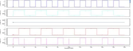
Simultaneous shield and repeater insertion
Fig. (11): ( dout1:- input to shielding, dout3:- output to shielding, dout4:- noise effect)
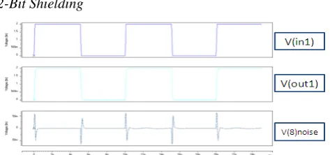
2-Bit Shielding
Fig. (12): 2Bit shielding output. (v(in), v(out), v( noise))
4 Bit UN Shielding
Fig. (13): UN shielding output (v (in) v (without buffer) v (with buffer)
Fig. (14): UN shielding output (v (in), v (with buffer), v (noise)
Multiplexer
Static power Dynamic power Delay Noise Without repeater insertion
152nw 7.10uW 2.78ns 600mv
With repeater insertion
152nw 7.10uW 0.60ns 600mv
Both shield and repeater insertion
586pW 511pW 0.1ns 11.5mv
Power Delay Noise
2 BIT SHIELDING static power :- 596nW dynamic power:-2.34uW 0.50nS 600mv 4 BIT UNSHIELD static power :- 152nw dynamic power :-7.10uW 0.60nS 600mV
Logic No. of
Transistors Avg. power With shielding Array Multiplier
2176 2.3mw 1.9mw
Wallace-tree multiplier
2120 1.8mw 1.5mw
Fulladder
Fig (16): Full adder with shielding
Observations Passive shielding
VI. CONCLUSION
The resource based optimization process is evaluated for a system that simultaneously considers shield and repeater insertion. The methodology is used to investigate power, delay, and noise tradeoffs. The noise performance is comparable among all of these techniques. With only shielding, however, the delay is higher, while in only repeater insertion, the power is higher. In practical cases where the delay, power, and area are constrained, simultaneous shield and repeater insertion exhibits the best performance. All these techniques are under passive shielding architecture. The optimal active shielding architecture uses shield driving circuits as multiplexer, full adder. The power dissipation and noise of active shielding architecture is decreases compare to passive shielding architecture. This was verified using Synopsys HSPICE circuit simulations.
R
EFERENCES Active shielding Table (I) Table (II) Table (III)[1] J. S. Choi and K. Lee,“Designof CMOS tapered buffer for minimum power–delayproduct,”IEEE J. Solid-State Circuits,
vol. 29, no. 9, pp.1142–1145, Sep. 1994.
[2] V. Kursun, R. M. Secareanu, and E. G. Friedman, “CMOS
voltage interface circuits for low power systems,”in Proc. IEEE
Int. Symp. Circuits Syst., May 2002, pp. 3.667–3.670.
[3] L. W. Linholm,“Anoptimized output stage for MOS integrated
circuits,”IEEE J. Solid-State Circuits, vol. SSC-10, no. 2, pp.
106–109, Apr. 1975.
[4] H. B. Bakoglu and J. D. Meindl, “Optimal interconnection circuits for VLSI,”IEEE Trans. Electron Devices, vol. ED-32,
no. 5, pp. 903–909, May 1985.
[5] J. Zhang and E. G. Friedman,“Crosstalk modeling for coupled
RLC interconnects with application to shieldinsertion,” IEEE Trans. Very Large Scale Integr. (VLSI) Syst., vol. 14, no. 6, pp.
641–646, Jun. 2006.
[6] Y. Massoud, J. Kawa, D. MacMillen, and J. White,“Modeling and analysis of differential signaling for minimizing inductive
crosstalk,”in Proc. ACM/IEEE Des. Autom. Conf., Jun. 2001, pp. 804–809.
[7] A. Carusone, K. Farzan, and D. A. Johns, “Differentialsignaling with a reduced number of signalpaths,”IEEE Trans. Circuits Syst. II, Analog Digital Signal Process. vol. 48, no. 3, pp. 294–
300, Mar. 2001.
[8] R. M. Secareanu and E. G. Friedman,“Transparentrepeaters,”in
Proc. IEEE Great Lakes Symp. VLSI, Mar. 2000, pp. 63–66. [9] A. Nalamalpu, S. Srinivasan, and W. Burleson,“Boosters for
driving long on-chip interconnects: Design issues, interconnect synthesis, and comparison with repeaters,” IEEE Trans. Comput.-Aided Design Integr. Circuits Syst., vol. 21, no. 1, pp.
50–62, Jan. 2002.
[10] K. Hirose and H. Yassura,“A bus delay reduction technique considering crosstalk,”in Proc. IEEE Des., Autom. Test Eur.
Conf. Exhib., Mar. 2000, pp. 441–445.
[11] B. Soudan,“Reducing mutual inductance of wide signal buses troughswizzling,”in Proc. IEEE Conf. Electron., Circuits, Syst., Dec. 2003, vol. 2, pp. 870–873.
[12] P. Gupta and A. Kahng, “Wire swizzling to reduce delay uncertainty due to capacitivecoupling,”in Proc. IEEE Int. Conf.
VLSI Des., Jan. 2004, pp. 431–436.
[13] M. A. El-Moursy and E. G. Friedman,“Wire shaping of RLC
A
UTHOR’
SP
ROFILEY. Sreenivasulu Goud was born at Kurnool, A.P, India on 2nd
June 1970. He received Bachelor degree in Electronics and Communication Engineering from MVSR Engg. College in 1993. He received his Master degree in software system from BITS pilani in 2000 and digital system and Electronics from JNTU. Anantapur, A.P in 2006. Currently he is pursuing his Ph.D. in Low Power VLSI System. He worked as faculty in ECE Dept. in G.Pulla Reddy Engg. College, Kurnool for 11 years. Presently he is working as associate professor and Head of ECE in Kottam College of Engg. Kurnool, A.P, India. He is having 15 yrs of teaching experience. His area of interest includes VLSI design and Low Power Testing.
M. Surendra Goud was born at Kadapa, A.P, India on 11th