Available at www.ijsred.com
ISSN : 2581-7175 ©IJSRED: All Rights are Reserved
Page 433
Design and Implementation of Low Power Area
Efficient Shift Register Using Modified Clock
Pulse Generator
Anitha.R
[1],
,Murugasami.R-ASP(ECE)
[2] Department of Electronics and communication Engineering,NandhaEngineering College, Erode
[1]
[email protected], [2][email protected]
Abstract—
Shift register is the key element to translate the parallel data to serial form or vice versa in digital circuits. It is commonly used in many applications, such as digital filters communication receivers, and image processing ASIC’s. It can also a function as delay circuits and digital pulse extenders. In the existing system, the conventional N-bit unidirectional shift-register was proposed and it consists of N number of master-slave flip-flop with multiple 2-to-1 multiplexers. Also, the conventional clock signal methodology was promoted to transfer data from one stage to next stage. It occupies more silicon area and increases the power consumption of the shift register. To eradicate the above said difficulties a novel 256-bit bidirectional shift-register using BD-PLs is proposed. It simplifies the BD-PL structure by removing the contemporary signals (Qb, DR_b, and, DL_b) and also reduce the number of full swing clock signals applied to each stage. The modified method will reduce area and power consumption of the bidirectional shift register. The proposed method will be implemented using the XILINX Software technology.
Index Terms—Area-efficient, bidirectional shift-register, flip-flop, pulsed clock, pulsed-latch.
I. INTRODUCTION
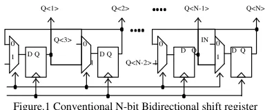
Bidirectional move registers are generally utilized in numerous applications, for example, advanced DC-DC buck converters [1], computerized low-dropout (LDO) controllers [2], decompressors [3], and advanced deferral bolted circles (DLL) [4]. Figure.1 demonstrates a customary N-bit bidirectional move register comprising of N ace slave flip-lemon and N 2-to-1 multiplexers. At the point when the bearing sign is '1', the bidirectional move register moves the information (Q<1:N>) right. Despite what might be expected, when the course signal is 0,it shifts the data left.
Figure.1 Conventional N-bit Bidirectional shift register
The regular bidirectional move register uses ace slave flip-flops comprising of two locks, appeared in Figure. 2(a). Its zone and power utilization can be decreased by supplanting the ace slave flip-flops with beat locks comprising of a hook and a beat clock signal, appeared in Figure. 2(b) [5]. In any case, the bidirectional move
register utilizing beat hooks can't share a beat clock signal, since all beat locks are empowered during clock beat width and this causes a race condition [5]. Hence, the bidirectional move register utilizing beat locks can't move the information right or left. Nonetheless, the move register utilizing beat hooks in [5] tackled this issue by utilizing sub move registers and extra transitory capacity locks. Be that as it may, despite everything it can't move the information left because of the invert request beat clock signals, regardless of whether the 2-to-1 multiplexers are included, for example, the ordinary bidirectional move register in Figure. 1. It additionally requires a long hold time to keep up the info signal.
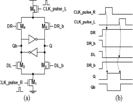
Figure .2 (a) Master Slave Flip-flop (b) Pulsed Latch
In this paper, a region productive bidirectional move register utilizing bidirectional beat locks is proposed. It can move the information right or left by utilizing proposed bidirectional beat hooks. It diminishes the territory and power utilization by supplanting Q<1> Q<2> Q<N-1> Q<N>
0 1
0 0
D Q D Q
0 D Q D Q
1 1 Q<N-2> 1
IN Q<3>
Available at www.ijsred.com
ISSN : 2581-7175 ©IJSRED: All Rights are Reserved
Page 434
expert slave flip-lemon and 2-to-1 multiplexers with proposed bidirectional beat locks and non-cover deferred beat clock signals. It additionally decreases the hold time to a clock beat width. The remainder of the paper is sorted out as pursues: Section II depicts the design of the proposed bidirectional move register. Segment III introduces the estimation aftereffects of the manufactured chip. At last, ends are attracted Section IV.
II. ARCHITECTURE
A.
Proposed Bidirectional Move Register UtilizingBidirectional Pulsed Latches
Figure3.(a)&(b) demonstrates the schematic and activity waveforms of the proposed bidirectional beat hook (BD-PL). The N-bit bidirectional move register can be acknowledged by interfacing the N BD-PLs in arrangement. The differential information contributions from the left hook (DL and DL_b) are associated with the differential information yields (Q and Qb) of the left lock. The differential information contributions from the correct hook (DR and DR_b) are associated with the differential information yields (Q and Qb) of the correct lock. At the point when the beat clock signal for right-moving or left-moving (CLK_pulse_R or CLK_pulse_L) is high, the hook information is refreshed to one side or right. In this way, the BD-PL stores the left or right hook information as indicated by CLK_pulse_R or CLK_pulse_L, individually. Figure.4 demonstrates the design of the bidirectional beat hook (BD-PL) involving 5.5µm2 with a 65nm CMOS process.
Figure.5 demonstrates the proposed 256-piece bidirectional move register utilizing BD-PLs. It applies sub move registers and extra brief hooks to lessen the quantity of the beat clock signals [5]. It improves the square of the BD-PL overlooking the integral sign (Qb, DR_b, and, DL_b) to clarify the activity effectively. It comprises of a bidirectional deferred beat clock generator, 64 4-piece sub bidirectional move registers, and an additional brief lock. The additional brief BD-PL is included front of the bidirectional move register so as to store the information signal (IN) for right-moving. The 4-piece sub bidirectional move register requires five BD-PLs to move information right or left by utilizing five beat clock signals for right-moving (CLK_pulse_R<1:4> and CLK_pulse_R<T>) or five beat clock signals for left-moving (CLK_pulse_L<1:4> and CLK_pulse_L<T>), individually. In the 4-piece sub bidirectional move register #1, four BD-PLs store 4-piece information
(Q<1>-Q<4>) and move the 4-piece information right or left. The transitory BD-PL stores Q<4> or the main BD-PL information (Q<5>) of the following sub bidirectional move register. Particularly, in the sub bidirectional move register #64, the transitory BD-PL stores the information signal (IN) for left-moving. The format of the 4-piece sub bidirectional move register can be drawn by associating five BD-PLs in Figure.4 on one side.
Figure.3(a) Schematic and (b) Operation waveform of proposed BD-BL
Available at www.ijsred.com
ISSN : 2581-7175 ©IJSRED: All Rights are Reserved
Page 435
Figure.5 Proposed 256-Bidirectional Shift Register Using Bidirectional Pulsed Latches
The proposed bidirectional shift-register stores IN to the temporary latch data T<1> or T<64> at the first pulsed clock signal. It can minimize the hold time (THOLD) of the input signal (IN). The pulsed clock signals are generated by the proposed bidirectional delayed pulsed clock generator in Figure. 7.The delay block is implemented with a 4-inverter chain.Figure.6 demonstrates the base clock process duration (TCLK_MIN) of the proposed bidirectional move register. TCLK_MIN is equivalent to TCP+5×TDELAY, where TCP is the deferral from the rising edge of the clock signal (CLK) to the rising edge of the first beat clock signal (CLK_pulse<T>), and TDELAY is the deferral of two neighboring beat clock signals.
Figure.6 Minimum Clock Cycle Time Of the Bidirectional Shift Register
Figure.7 Proposed Bidirectional Delayed Pulsed Clock Generator
B. Chip Implementation
Available at www.ijsred.com
ISSN : 2581-7175 ©IJSRED: All Rights are Reserved
Page 436
procedure corner recreations (FF-SS). The clock beat width (TPULSE) is intended to 75ps by including the rising and falling times (15ps and 15ps) and a planning edge (15ps) to the least clock beat width (30ps). The beat clock delay (TDELAY) is 100ps, controlled by including the non-cover time of 25ps between two neighboring heartbeat clock signals. From the start, CLK_pulse_R<T> refreshes the transitory information T<1> to Q<4>. At that point, CLK_pulse_R<1:4> update the 4-piece information Q<1>-Q<4> in the turnaround request.
B. Performance Comparison
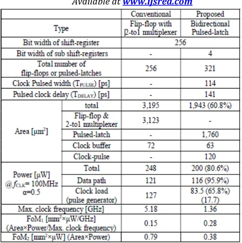
Table 1 demonstrates the exhibition examinations of the ace slave flip-flop with 2-to-1 multiplexer (MSFF) and delay bidirectional beat lock (BD-PL). The MSFF and BD-PL were executed with a 65nm CMOS process. The schematics of the ace slave flip-flop with 16 transistors also, the 2-to-1 multiplexer with 6 transistors. It evacuates the information and yield supports (inverters) in 2-to1 multiplexer to limit the quantity of the transistors, in light of the fact that the yield inverter of the ace slave flip-lemon can fill in as the info support. The clock signals CLK and CLK_b are driven by worldwide clock supports rather than inward clock cradle to decrease the territory. For correlation, the spans of both NMOS and PMOS transistors are 0.21µm/0.06µm, which is the base transistor size. The MSFF design region is 12.2µm2, which was drawn by sharing every single imaginable source and depletes of its transistors. The BD-PL decreases the territory by 54.9% contrasted with the MSFF. The forces were estimated at fCLK=100MHz with VDD=1.2V, when the information change proportion (α) is 0.5. The BD-PL decreases the power utilization by 64.9% contrasted with the MSFF.
Table1. Performance comparison of the MSFF and BD-PL
Table2. Performance Comparison of the 256-bit Bidirectional Shift Register
Table.2 demonstrates the exhibition examinations of the 256-piece bidirectional move registers. The post-design reproduction was performed to incorporate the parasitic parameters. The ordinary bidirectional move register utilizes 256 ace slave flip-flops and 256 2-to-1 multiplexers. The proposed bidirectional move register requires 321 bidirectional beat hooks, because of the impermanent locks appeared in Figure. 4. The clock burden intensity of the proposed bidirectional move register incorporates the intensity of the bidirectional postponed beat check generator in Figure. 7. The proposed bidirectional move register decreases the territory and power utilization by 39.2% what's more, 19.4% contrasted with the regular bidirectional move register, individually. For the exhibition examination, two figure-of-merits (FoM1 and FoM2) are utilized. The proposed bidirectional move register has the huge FoM1(=Area×Power /Max. clock recurrence) because of its low max. clock recurrence. Be that as it may, it has little FoM2(=Area×Power), in light of the fact that the clock recurrence is fixed at the most applications.
Table 3 demonstrates the execution correlations of the 256-piece bidirectional move registers as per the procedure, supply voltage, and temperature (PVT) varieties.The proposed 256-piece bidirectional move register was created utilizing a 65nm CMOS process. Table.3 records the execution examinations of the bidirectional move register chips.
Available at www.ijsred.com
ISSN : 2581-7175 ©IJSRED: All Rights are Reserved
Page 437
III. SIMULATION RESULTS
Figure.6 demonstrates the activity waveforms of the 256-piece bidirectional move register when right-moving and left-moving. At the point when right-moving, CLK_pulse_R<T> first updates the transitory information T0 to the information signal (IN). At the same time, in the sub bidirectional move register #1, the impermanent information T<1> is refreshed to Q<4>.
Figure.8 Simulation Results of Bidirectional Shift Register When Clock Generation
And afterward, the lock information Q<4>-Q<2> are consecutively refreshed to one side lock information Q<3>-Q<1>. At last, the main hook information Q<1> is refreshed to T<0>, which holds the information signal (IN). Other sub bidirectional move registers work similarly as the sub bidirectional move register #1. Then again, when left-moving, the hooks aside from the brief locks work in the turnaround request of the right-moving. Along these lines, the proposed bidirectional move register can move information to one side or then again to one side. In this paper, a region
Available at www.ijsred.com
ISSN : 2581-7175 ©IJSRED: All Rights are Reserved
Page 438
Figure.9 Simulation Results of Bidirectional Shift Register When Left Shifting
Figure.10 Simulation Results of Bidirectional Shift Register When Right Shifting
Available at www.ijsred.com
ISSN : 2581-7175 ©IJSRED: All Rights are Reserved
Page 439
control utilization by supplanting expert slave flip-flops what's more, 2-to-1 multiplexers with the proposed bidirectional beat hooks and deferred beat clock signals, and by utilizing sub move registers and additional transitory stockpiling locks. A 256-piece bidirectional move register was manufactured utilizing a 65nm CMOS process. Its zone is 1,943µm2. Its capacity utilization is 200µW-100µW when the information change proportion is 1/2-1/16 at a 100MHz clock recurrence with VDD=1.2V. It decreases region by 39.2% and control utilization by 19.4% contrasted with the traditional bidirectional move register.
REFERENCES
[1] X. Zhang, et al., “A 0.6 V Input CCM/DCM Operating Digital Buck Converter in 40 nm CMOS,” IEEE Journal of Solid-State Circuits, vol.49, no. 11, pp. 2377–2386, Nov. 2014.
[2] M. Huang, et al., “A Fully Integrated Digital LDO With Coarse–Fine-Tuning and Burst-Mode Operation,” IEEE Transactions on Circuits and Systems II: Express Briefs, vol. 63, no. 7, pp. 683-687,Jul. 2016.
[3] B.-D. Yang, “Low-Power and Area-Efficient Shift Register Using Pulsed Latches,” IEEE Transactions on Circuits and Systems I: Regular Papers, vol. 62, no. 6, pp. 1564–1571, Jun. 2015.
[4] Tingting. Yu, et al., “ A New Decompressor with Ordered Parallel Scan Design for Reduction of Test Data and Test Time,” 2015 IEEE International Symposium on Circuits and Systems (ISCAS), May. 2015, pp. 24-27.
[5] Keerthi. K. M, et al, “ Design of FinFET based All-Digital DLL for multiphase clock generation,” 2015 Annual IEEE India Conference (INDICON), Dec. 2015, pp. 17-20.
[6] H. Partovi et al., “Flow-through latch and edge-triggered flip-flop hybrid elements,” IEEE Int. Solid-State Circuits Conf. (ISSCC) Dig. Tech. Papers, pp. 138–139, Feb. 1996. [7] E. Consoli, M. Alioto, G. Palumbo, and J. Rabaey,
“Conditional push-pull pulsed latch with 726 fJops energy delay product in 65 nm CMOS,” in IEEE Int. Solid-State Circuits Conf. (ISSCC) Dig. Tech. Papers, Feb. 2012, pp. 482–483.
[8] V. Stojanovic and V. Oklobdzija, “Comparative analysis of masterslave latches and flip-flops for high-performance and low-power systems,” IEEE J. Solid-State Circuits, vol. 34, no. 4, pp. 536–548, Apr. 1999.
[9] S. Heo, R. Krashinsky, and K. Asanovic, “Activity-sensitive flip-flop and latch selection for reduced energy,” IEEE Trans. Very Large Scale Integr. (VLSI) Syst., vol. 15, no. 9, pp. 1060–1064, Sep. 2007