A Thesis Submitted for the Degree of PhD at the University of Warwick
http://go.warwick.ac.uk/wrap/38432
This thesis is made available online and is protected by original copyright. Please scroll down to view the document itself.
Interface modification in organic and
hybrid photovoltaics
A thesis submitted for the degree of
Doctor of Philosophy
at The University of Warwick
by
Stefan Schumann
Supervised by Prof. Tim S. Jones
Department of Chemistry
The University of Warwick, Coventry
Abstract
With the growing importance of organic photovoltaics (OPVs) as an attractive, low cost and sustainable energy source the field has been investigated intensively, showing high potential for commercialisation. To further improve device performance, different routes of development have been explored targeting interfaces that play a crucial role in device performance including the donor (D)/acceptor (A) and electrode/photoactive layer interfaces, as well as incorporation of new materials.
Vertical co-deposition of water-soluble small molecule copper(II) phthalocyanine-tetrasulfonic acid tetrasodium salt (TSCuPc) and polymeric sodium poly[2-(3-thienyl)ethoxy-4-butylsulfonate] (PTEBS) with polystyrene (PS) nanospheres to template, followed by solvent vapour sphere removal, is shown as an excellent method to generate three-dimensionally ordered macroporous large area thin films of sub-100 nm pore size. After a subsequent infiltration by the electron acceptor phenyl-C61-butyric acid methyl ester (PCBM), three-dimensionally (3D) interdigitated D-A composite structures are generated which are further implemented in complete OPV devices. PTEBS based 3D nanostructured D-A composite devices reached a comparable performance to planar reference devices but did not show the expected photocurrent improvement. This is most likely due to the complexity of this multistep fabrication method and the large probability if impurities in the films. However, it demonstrates a new approach towards nanoengineered 3D interdigitated organic D-A composite OPV devices.
A substantial increase in device performance and operational stability in solution processed inverted bulk heterojunction (BHJ) OPVs is demonstrated by introducing a zinc oxide (ZnO) or titanium oxide (TiOx) interlayer between the electron collecting bottom electrode and the photoactive blend of poly(3-hexylthiophene) (P3HT) and PCBM. The introduction of transition metal oxide (TMO) interlayers resulted in a remarkable increase in power conversion efficiency (PCE) with a maximum value of 4.91 %. The structure and morphology of the dense, planar ZnO layers was controlled either by electrodeposition or spray pyrolysis techniques.
Table of contents
Abstract ... ii
Table of contents ... iv
Declaration... vii
Acknowledgements ... viii
List of publications and presentations ... ix
List of abbreviations ... xi
List of symbols and notations... xiii
List of compounds ... xv
Chapter 1: Introduction ... 1
1.1 General overview ... 1
1.1.1 The need for PVs ... 1
1.1.2 Background to PVs ... 2
1.1.3 Development of OPVs ... 4
1.2 Semiconductor and device theory ... 6
1.2.1 Condensed matter... 7
1.2.2 Principle of operation ... 10
1.3 Materials and properties ... 17
1.3.1 Electron donor materials ... 18
1.3.2 Electron acceptor materials ... 21
1.3.3 Interlayer and electrode materials ... 23
1.4 Device interface modification and nanostructuring ... 25
1.4.1 D/A interface modification ... 25
1.4.2 TMO interlayers ... 29
1.4.3 Hybrid OPVs ... 31
1.5 Project motivation and thesis outline ... 32
Chapter 2: Experimental and analysis ... 35
2.1 Thin film and device fabrication ... 35
2.1.1 Material purification ... 35
2.1.2 Substrate cleaning ... 37
2.1.3 Solution processed thin films ... 37
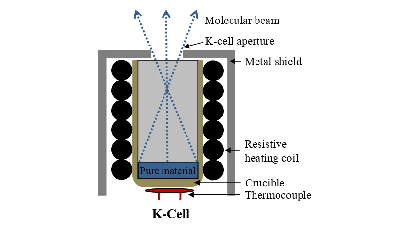
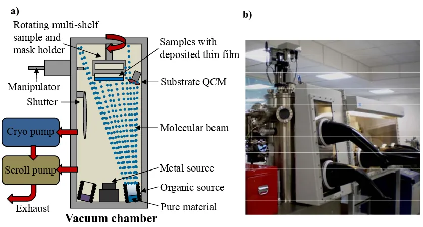
2.1.4 Organic molecular beam deposition (OMBD) ... 40
2.2 Thin film analysis ... 46
2.2.1 Atomic force microscopy (AFM) ... 47
2.2.2 Electron microscopy (EM) ... 49
2.2.3 Electronic absorption spectroscopy ... 55
2.2.4 X-ray diffraction ... 56
2.3 PV device analysis ... 58
2.3.1 The sun and solar simulation ... 59
2.3.2 J-V characteristics ... 61
2.3.3 External quantum efficiency (EQE) measurement ... 65
3.1 Introduction ... 68
3.1.1 Definitions... 68
3.1.2 Emulsion polymerisation ... 69
3.1.3 Dynamic light scattering (DLS) ... 72
3.1.4 Aim ... 73
3.2 Experimental ... 74
3.2.1 Nanosphere synthesis ... 74
3.2.2 Sphere size characterisation and solid content measurement ... 77
3.3 Results ... 78
3.3.1 Nanosphere synthesis in the round-bottom flask ... 78
3.3.2 Reactor based nanosphere synthesis ... 82
3.4 Conclusion ... 87
Chapter 4: Planar heterojunction devices ... 89
4.1 Introduction ... 89
4.1.1 Solution processed TSCuPc ... 89
4.1.2 Solution processed PTEBS ... 90
4.1.3 Aim ... 91
4.2 Experimental ... 92
4.3 Results ... 93
4.3.1 TSCuPc thin film based OPV devices ... 93
4.3.2 PTEBS thin film based OPV devices... 101
4.3.3 Device stability ... 108
4.3.4 Film surface treatment ... 109
4.4 Conclusion ... 111
Chapter 5: 3D interdigitated organic D-A composite structures and OPV devices 114 5.1 Introduction ... 114
5.1.1 Background ... 114
5.1.2 Colloidal crystals and templating... 115
5.1.3 Nanosphere self-assembly ... 116
5.1.4 Organic 3D open-cellular and composite nanostructures ... 119
5.1.5 3D nanostructured composite OPV devices ... 120
5.1.6 Aim ... 122
5.2 Experimental ... 123
5.2.1 Open-cellular organic thin films ... 123
5.2.2 Fabrication of 3D nanostructured composite devices ... 125
5.3 Results ... 126
5.3.1 Open-cellular organic semiconductor thin films ... 126
5.3.2 D-A 3D nanostructured composite OPV devices ... 134
5.4 Conclusions ... 141
Chapter 6: Electrode modification through TMO interlayers ... 144
6.1 Introduction ... 144
6.1.1 Background of TMO interlayers in OPVs ... 144
6.1.2 Aim ... 147
6.2 Experimental ... 147
6.2.1 TMO interlayer preparation and characterisation ... 147
6.3 Results ... 149
6.3.1 Transmission ... 149
6.3.2 Morphology... 149
6.3.3 XRD ... 151
6.3.4 OPV device performance ... 153
6.3.5 Conclusions ... 164
Chapter 7: Planar inorganic/organic hybrid devices ... 166
7.1 Introduction ... 166
7.1.1 Background of TMO/organic hybrid OPVs ... 166
7.1.2 Aim ... 167
7.2 Experimental ... 168
7.3 Results and discussion ... 168
7.3.1 Electronic absorption and transmission ... 168
7.3.2 Morphology... 169
7.3.3 OPV device performance ... 171
7.3.4 EQE and device structure comparison ... 176
7.3.5 Device stability ... 178
7.4 Conclusion ... 181
Chapter 8: Conclusions and further work ... 183
8.1 Conclusions ... 183
8.1.1 Nanosphere synthesis ... 183
8.1.2 Planar heterojunction devices ... 184
8.1.3 3D interdigitated organic D-A composite structures and OPV devices ... 185
8.1.4 Transition metal oxide (TMO) interlayers ... 186
8.1.5 Planar inorganic/organic hybrid devices ... 187
8.2 Further work ... 188
Declaration
The work presented in this thesis has been conducted by myself at the Department of Chemistry at The University of Warwick in Coventry except the following experiments in Chapter 6. All zinc oxide thin films were deposited and characterised by Dr. Benoit Illy at the Department of Materials at Imperial College London, including X-ray diffraction and light transmission studies. The transmission electron microscopy cross-section images of complete photovoltaic devices, fabricated by focused ion beam/ scanning electron microscopy in Chapter 6 were also prepared and taken by Dr. Illy. Part of this work was supervised by Prof. David McComb who is also at the Department of Materials at Imperial College London. I confirm that none of the work included has previously been submitted for a higher degree.
Acknowledgements
Firstly, I would like to thank my supervisor Professor Tim Jones for his support and guidance through my PhD. Tim gave me the great opportunity to conduct research in a scientific area, which had fascinated me already for a long time during my undergraduate studies. I hope with this project, I was able to make a contribution towards the big dream of human kind to exploit the sun’s enormous energy potential to realise a sustainable future energy supply. At the same time, I am grateful to the Department of Chemistry at The University of Warwick for providing such excellent research facilities as well as a stimulating atmosphere and my industrial sponsor BP Solar for their funding.
The person, I would like to thank in particular for his great help, support and advice, is my post-doc Dr. Paul Sullivan. Thanks also go to Dr. Raffaello da Campo, who was involved in all the work conducted in collaboration with Imperial College London. It should not be forgotten all the help, support and fruitful discussions, but also great tea breaks I had with all the other members of my research group: Ian Hancox, Virendra Chauhan, Nicola Beaumont, Tom Howells, Luke Rochford, Edd New and Dr. Junliang Yang.
Here in our department, I would like to thank Dr. Ross Hatton as well as Dr. Stefan Bon and their research groups for a great collaboration and valuable inputs. Thanks also go to Steve York and Richard Beanland in the electron microscopy group in Physics for all their time for training and help.
At Imperial College London great thanks go to Dr. Benoit Illy, Dr. Amy Cruickshank, Dr. Mary Ryan, Prof. David McComb and Dr. Jason Riley at the London Centre of Nanotechnology (LCN) for the close collaboration and supply of zinc oxide (ZnO) substrates as well as Dr. Martyn McLachlan and now Dr. Sarah Berhanu for their help and inputs on the nanosphere project.
List of publications and presentations
Publications:
• S. Schumann, S. A. F. Bon, R. A. Hatton and T. S. Jones, Open-cellular organic
semiconductor thin films by vertical co-deposition using sub-100 nm nanosphere templates,Chemical Communications, 2009, 6478-6480.
• S. Schumann, R. Da Campo, B. N. Illy, A. C. Cruickshank, M. A. McLachlan,
M. P. Ryan, D. J. Riley, D. W. McComb and T. S. Jones, Inverted organic photovoltaic devices with high efficiency and stability based on metal oxide charge extraction layers, Journal of Materials Chemistry, 2011, 21, 2381-2386.
• S. Schumann, R. A. Hatton and T. S. Jones, Organic Photovoltaic Devices Based
on Water-Soluble Copper Phthalocyanine, Journal of Physical Chemistry C, 2011, 10.1021/jp109544m.
• B. N. Illy, A. C. Cruickshank, S. Schumann, R. Da Campo, T. S. Jones, S. Heutz,
M. A. McLachlan, D. W. McComb, D. J. Riley and M. P. Ryan, Electrodeposition of ZnO layers with controllable thickness and orientation and their applications as electron extracting interlayer in organic photovoltaics, Journal of Materials Chemistry, submitted.
• A. C. Cruickshank, S. E. R. Tay, B. N. Illy, R. Da Campo, S. Schumann, T. S.
Jones, S. Heutz, M. A. McLachlan, D. W. McComb, D. J. Riley and M. P. Ryan, Electrodeposition of Nanostructured ZnO Films onto Organic Thin Films, Chemistry of Materials, submitted.
• S. Schumann, C. Dearden, T. Howells, R. Pitt, R. Da Campo, P. Sullivan and T.
S. Jones, Hybrid organic-inorganic solar devices based on the small molecule organic semiconductor boron subphthalocyanine chloride, to be submitted.
• S. Schumann, R. A. Hatton and T. S. Jones, Organic photovoltaic devices based
on water-soluble polythiophene, to be submitted.
• S. Schumann, R. A. Hatton and T. S. Jones, 3D nanostructured donor-acceptor
composite organic photovoltaic devices by colloidal templating, to be submitted.
Patents:
• S. Schumann, R. A. Hatton, T. S. Jones, Templating films, GB090840.5, 2010
Presentations:
• BP Solar industrial sponsor meetings, Imperial College London, 2007-2010
• Excitonic solar cells 2009, University of Warwick, August 2008, Poster
• Postgraduate Research Symposium 2009, University of Warwick, June 2009, Poster
• BP Solar OPV workshop, Washington DC, Dulles (USA), July 2009, Talk
• IUPAC Congress, Glasgow, August 2009, Talk
• MRS Fall 2009, Boston (USA), December 2009, Talk
• CMMP 2009, University of Warwick, December 2009, Poster
• Postgraduate Research Symposium 2010, University of Warwick, June 2010, Talk First prize
• Bristol Nanoscience Symposium 2010, University of Bristol, September 2010, Poster
• Research Council UK, University of Oxford, October 2010, Poster
List of abbreviations
3DOM Three-dimensionally ordered macroporous solids (A)/D (Acceptor)/donor
AFM Atomic force microscopy
AM Air mass
AO Atomic orbital
BE Binding energy
BHJ Bulk heterojunction
BSE Backscattered electrons
CB Conduction band
(D)/A (Donor)/acceptor
DLS Dynamic light scattering
DSSC Dye-sensitised solar cell
ED Electrodeposition
EM Electron microscopy
FEG Field emission gun
(O)FET (Organic) field effect transistor
FIB Focused ion beam
HOMO Highest occupied molecular orbital
HV High vacuum
(N)IR (Near) infrared light
(O)LED (Organic) light emitting diode LUMO Lowest unoccupied molecular orbital MIS Metal-insulator-semiconductor
MO Molecular orbital
NSL Nanosphere lithography
OMBD Organic molecular beam deposition
PBG Photonic bandgap
(O)PV (Organic) photovoltaic QCM Quartz crystal microbalance
RH Relative humidity
SAM Self-assembled monolayer
SE Secondary electrons
SEM Scanning electron microscopy
SP Spray pyrolysis
SPM Scanning probe microscopy
STM Scanning tunnelling microscopy
UV Ultraviolet light
VB Valence band
vdW Van der Waals
vis Visible light
List of symbols and notations
φ Workfunction
Å Angstrom (1 Å = 0.1 nm)
BE(exc.,gem.) Exciton binding energy, geminate pair binding energy
c Concentration
d Actual film thickness
dhkl Lattice plane spacing or interplanar spacing of plane (hkl)
D Diffusion coefficient
ε Dielectric constant
E(F) (Fermi) energy
EG Energy bandgap
E(EA,IP) Electron affinity, ionisation potential
EVac Vacuum energy level
EQE External quantum efficiency
f(E) Fermi-Dirac distribution
F(hd,ic) Hydrodynamic force, immersion capillary force
FF Fill factor
(hkl) Miller indices
IPCE Incident photon conversion efficiency
ϕAM Incident angle (sun light)
J(dark,ph) Dark current density, photo current density
J(SC) (Short-circuit) current density
Jmp Current density at maximum power point
J-V Current density-voltage
λ Wavelength
LD Exciton diffusion length
η(abs,ed,ct,cc) Quantumefficiency of photon absorption and exciton formation, exciton
Pmp Operational maximum power output
PCE Power conversion efficiency
r(B,C) Bohr radius, Coulomb radius
R(l,s,sh) Load resistance, series resistance, shunt resistance
Rq Surface roughness parameter
s Step edge thickness, actual film thickness
S(0,1) First singlet ground state, excited state
θ Angle of incidence (XRD)
T Temperature
T(λ) Transmission
TC(hkl) Texture coefficient of (hkl)
τ Life time
V(OC) (Open-circuit) voltage
Vmp Voltage at maximum power point
Structure notation
A(m)/B(n) Layer of compound A with the actual thickness m in brackets covered by a layer of compound B with an actual thickness n A:B Blend of compound A with compound B
List of compounds
AMPAD 2,2’-azobis(2-methylpropion amidine) dihydrochloride
BCP 2,9-dimethyl-4,7-diphenyl-1,10-phenantroline (bathocuproine)
C60 Buckminster fullerene
CuPc Copper phthalocyanine
H2Pc Metal-free phthalocyanine
ITO Indium-tin oxide
KPS Potassium persulfate (K2S2O8)
MEH-PPV Poly(2-methoxy-5-(2’-ethyl-hexyloxy)-p-phenylene vinylene)
MoOx Molybdenum oxide
MWCNT Multiwall carbon nanotube
NaSS Styrene-4-sulfonic acid sodium salt
NH3 Ammonia
P3HT Poly(3-hexylthiophene)
(M)Pc (Metal) phthalocyanine
PCBM Phenyl-C61-butyric acid methyl ester
PEDOT:PSS Poly(3,4-ethylenedioxythiophene) poly(styrene sulfonate) PPV Poly(phenylene)vinylene
PS Polystyrene
PTEBS Sodium poly[2-(3-thienyl)ethoxy-4-butylsulfonate]
SDS Sodium dodecyl sulphate
SubPc Boron subphthalocyanine chloride
TCO Transparent conducting oxide
THF Tetrahydrofuran TiO(x/2) Titanium oxide, titanium dioxide
TMO Transition metal oxide
TSCuPc 3,4’,4’’,4’’’-copper phthalocyanine-tetrasulfonic acid tetrasodium salt
WOx Tungsten oxide
Chapter 1:
Introduction
In this chapter a general overview is given of the need of photovoltaic (PV) and organic photovoltaic (OPV) devices in particular, including the background and challenges. The general theory and concepts of semiconductors and devices are also explained. Furthermore, the materials used and their properties are explained in detail. Another section covers the concept of interface modification including template assisted nanostructuring, the use of electrode interlayers and hybrid device structures. The chapter is closed with an outline of the project motivation and the thesis content.
1.1
General overview
This section covers the world’s energy challenge and how PVs, and more specifically OPVs, can contribute to a sustainable solution. In a general background section the different types of PVs are broadly explained dividing them into three technology generations, with OPVs being the least advanced. More details on OPV development and its challenges are revealed in the last section.
1.1.1
The need for PVs
With increasing world population and growing industrial use a steep increase in global energy demand is unavoidable. Conventional energy sources, including fossil fuels such as oil, gas and coal are limited in supply, and the predicted production peak is likely to be reached soon. With combustion based energy supply come two of the biggest threats to human and animal health: air pollution and greenhouse gases associated with global warming.[1] Emitted carbon dioxide (CO
2) is a greenhouse gas and one of the main contributors to global warming, which has already led to a rise of the earth’s global mean surface temperature by 0.6 °C during the twentieth century.[2]
Chapter 1: Introduction
are required including hydro, wind, wave, tidal, biomass, geothermal and solar power.[3, 4] Most of these technologies are either directly or indirectly fuelled by the sun, which is the only non-polluting renewable energy source available to mankind on a sufficient scale to cover present and future demand. PV devices offer an amazing potential to harvest and convert solar power into electricity due to their great flexibility and compatibility for powering portable devices and local grids to the attachment to buildings, modern transport vehicles, including solar cars, boats and even airplanes, but also applications in space technology.[5]
The current challenge is to overcome the high energy input and fabrication cost involved in the production of PV devices. OPVs offer the potential of a new low-cost renewable solar PV technology which could potentially lead to such a large-scale application.[6]
1.1.2
Background to PVs
Edmund Bequerel discovered the photovoltaic effect in 1839, but it took a further 100 years until the first successful PV devices were developed. After the discovery and development of p-n junction doping in crystalline silicon and progress in the fabrication of high quality silicon wafers in the 1950s, this technology rapidly developed into a relatively efficient, commercialised energy source.[7] With silicon solar technology based on doped group IV semiconductors the first generation of PVs was born with two more generations to follow.
Conventional inorganic solar panels for terrestrial use are based on mono- or poly-crystalline p-n doped silicon with efficiencies of up to 25 %,[8] but latest technologies have already passed this limit (see Figure 1.1)[9]. Crystalline silicon cells require a high energy input for large-scale production with high fabrication costs. Amorphous silicon with much lower fabrication cost can also be employed but leads to a lower cell efficiency of ~10 %.[8]
the growth of thin inorganic films which can be tailored in absorption behaviour to the solar spectrum.[10] High efficiencies have been reached with multijunction III-V cells with around 36 %.[8] Major drawbacks are the low abundance and high toxicity of certain elements used in the cells.
[image:19.595.88.517.386.679.2]The latest generation of PVs are organic and organic/inorganic hybrid PVs which rely on stable exciton formation and efficient exciton diffusion. The cells usually employ at least one organic electron donor material in the form of a dye or chromophore thin film to harvest sun light. In most types of OPVs an organic compound is also employed as an electron acceptor material. All organic compounds consist mainly of the elements carbon, nitrogen, oxygen and hydrogen with variations of metals in complexes and other elements. The main advantages of this emerging generation are the use of low-cost compounds and fabrication technology, as well as favourable properties such as flexibility, non-toxic materials and low overall weight.[11]
Figure 1.1 Development of PV devices including OPVs quoting the efficiencies for different technologies
Chapter 1: Introduction
Excitonic solar cells or OPVs can be divided into three main categories: dye-sensitised solar cells (DSSC), OPVs based on either small molecules or polymers, and hybrid organic/inorganic OPVs. The development of most PV technologies is summarised in Figure 1.1.[9]
DSSCs were initially invented in 1991 by O’Regan and Graetzel and reached an early record of 12 % power conversion efficiency (PCE).[12] The concept is based on a photo-electrochemical PV cell with a dye as a photon acceptor and electron donor, titanium dioxide (TiO2) as an electron acceptor and an electrolyte to enable redox chemistry and charge transfer between the photo-sites and the electrode.[13, 14] All other solid state OPVs are explained in detail in the following sections.
1.1.3
Development of OPVs
solar cells, a material which was discovered by Kroto et al. in 1985.[18] C60 makes an ideal electron acceptor and provides a relatively large exciton diffusion length, LD.[19]
By employing C60 in a heterojunction device architecture, the organic solar device performance increased significantly. In the last few years, devices employing vacuum deposited small molecules, such as phthalocyanines, subphthalocyanines, anthracenes and oligothiophenes reached device efficiencies of up to 5.2 %.[20-23]
One of the crucial efficiency limiting factors in OPVs is the relatively short LD in the range of a few tens of nanometres in polycrystalline organic semiconductors as photo-generated excitons have to reach the heterojunction interface for efficient exciton dissociation before recombining.[24-26] A more detailed description can be found in Section 1.2.2. Therefore, a main part of organic heterojunction device performance optimisation is to find a compromise of the film thickness required for maximum absorbance and the limited LD for efficient exciton dissociation.[26, 27] This problem is also the main limiting factor of simple planar bilayer OPV devices.
By stacking two or more cells with the same or complementary optical band gaps in a tandem arrangement equipped with just a thin recombination layer, the layer thickness in the individual cells can be kept thin to match LD with increased light absorption in the additional layers. The series connection of the cells leads to an increase in open-circuit voltage (VOC).[28, 29] Therefore, the efficiency can be significantly improved as demonstrated for small molecules by Cheyns et al. with 5.2 %[30] and Heliatek with 8.3 %,[31] as well as for polymer/fullerene systems by Sista et al with 5.8%[32] and by Kim et al. with 6.5 %[33] reported for all-solution processed tandem devices.
Chapter 1: Introduction
area allowing higher charge separation efficiency with extremely fast electron transfer from the donor to the acceptor.[39] This resulted in a very rapid development in BHJ OPV technology with the photoactive blend of poly(3-hexylthiophene) (P3HT) and phenyl-C61-butyric acid methyl ester (PCBM) being the most studied system.[40-42] Polymer design has recently been directed at increasing VOC through intelligent tuning of the energy level difference between the highest occupied molecular orbital (HOMO) energy of the electron donor and the lowest unoccupied molecular orbital (LUMO) energy of the electron acceptor, whilst also optimising light absorption across the solar spectrum.[43-45]. This development has resulted in PCEs as high as 7.4 %.[46]
A different approach to solve the LD problem was a D/A mixed layer system fabricated by co-deposition with organic molecular beam deposition (OMBD), providing an interpenetrating D/A interface. This was first introduced by Hiramoto,[47] with Sullivan and Heutz et al. undertaking further investigations with particular focus on mixed layer compositions in the CuPc/C60 system.[48, 49] Very high device performance efficiencies of 5 % were later reported by Xue et al. using this approach.[50]
Despite the overall performance improvement in both BHJ and mixed layer structures through enhanced exciton diffusion efficiency, charge transport is compromised due to the random nature of these mixed structures.[26] To overcome this problem a more controlled interpenetrating D/A composite structure is required that has the advantages of mixed layers, but with well structured charge transport paths. OPV device limitations and new approaches to tackle this issue are discussed in detail in section 1.4.
Although good progress has been made in recent years, OPVs are at the moment still not able to compete with inorganic PVs in their PCE. However, despite this lower efficiency, the cheaper materials and lower manufacturing costs could make them competitive in the near future, with good market potential.[51]
1.2
Semiconductor and device theory
defined the same way using similar concepts and conventions. In order to understand organic/organic and organic/inorganic heterojunctions, so called hybrid heterojunctions, as well as the resulting OPV devices, semiconductor theory and its implementation in OPVs is explained in the following sections.[52, 53]
1.2.1
Condensed matter
Chapter 1: Introduction
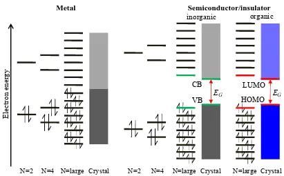
[image:24.595.91.502.188.443.2]increased temperature due the population of the CB by thermally excited electrons (EG < kBT). This creates vacancies, positively charged holes, in the VB. For insulators the band gap is too large to be overcome by thermal excitation making charge flow impossible.
Figure 1.2 As the number of atoms, N, increases towards a cluster and then a crystal, the AOs split first
into discrete, later merged multiple energy levels and finally form bands. In a metal the bonding and anti-bonding bands are overlapping. In a semiconductor or insulator of organic or inorganic nature, the bands or MOs are separated by an energy bandgap, EG.
As shown in Figure 1.3 the CB edge energy level of a semiconductor is defined by the electron affinity (EEA) of the material measured from the vacuum level (EVac). EEA is defined as the least amount of energy needed to remove an electron from a singly charged negative ion or from the solid to the vacuum level. In other words, it describes how easy an electron can be accepted by the solid. EVac is the energy level at which an electron from the solid is far enough away such that it does not experience any interaction forces from the solid. The VB edge is defined by the ionisation potential (EIP), also measured from the vacuum level. EIP is the least energy required to remove an electron from an atom or molecule in its electronically neutral ground-state.
Electron ener
gy
N=2 N=4 N=large Crystal
Semiconductor/insulator
N=2 N=4 N=large Crystal
Metal
EG
N=large Crystal EG
inorganic organic
VB CB
Figure 1.3 Band profiles of a metal and different types of semiconductors: intrinsic, n-type and p-type.
The likelihood of an electron being found in a certain level with energy E, is defined by the Fermi-Dirac probability distribution function, f(E), shown in Equation 1.1,
Equ. 1.1
where kB is Boltzmann’s constant, EF is the Fermi energy or Fermi level, and T is the temperature. EF is the theoretical energy level at which the population probability of an electron is 0.5. This is of special importance for both metals and semiconductors and plays a major role in further semiconductor classification. Another important material
parameter linked to EF is the workfunction φw, which is defined as the potential required to remove the least bound electron (Equation 1.2).
Equ. 1.2
For metals EF defines the band edge of the VB and CB due to band overlap and the workfunction of the metal, φm, is equal to EIP.
Semiconductors can be divided into two classes; intrinsic and extrinsic semiconductors (see Figure 1.3). Extrinsic semiconductors can further be split into n-type and p-type. Intrinsic semiconductors are assumed to be perfect crystals without any defects or impurities. At equilibrium, the E is situated exactly midway between the VB
Semiconductor Metal
El
ectr
on
ener
gy/
eV
EVac= 0
Vacuum
level intrinsic n-type p-type
VB CB
VB CB
VB CB
EF
(VB = CB)
ECB
EVB
EF
EF
EF
EG
Φi Φn Φp Φm=EIP
EIP
Chapter 1: Introduction
and CB in an inorganic semiconductor and between the HOMO and LUMO in an organic
semiconductor with a workfunction φi. All organic semiconductors if not doped in any way are considered to be intrinsic semiconductors. n-type semiconductors are semiconductors doped with impurities which provide additional valence electrons to the host material. These impurities establish occupied energy levels close to the CB which also acts as an electron donor level. As a consequence, EF is shifted between these induced electron donor energy levels and the CB. Equally, when an intrinsic semiconductor is doped with hole-rich and therefore electron accepting impurities, an acceptor energy level is established close to the VB with EF being situated in between. The workfunction of an n-type semiconductor (φn) is lower and the workfunction of a
p-type semiconductor (φp) is higher than the φi of its equivalent undoped intrinsic semiconductor.
1.2.2
Principle of operation
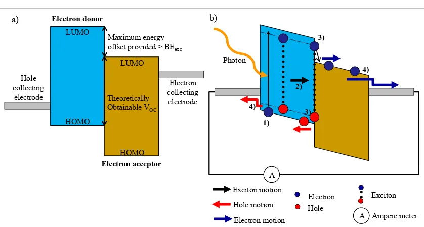
A typical heterojunction bilayer OPV device with its energy level schematic in open circuit condition can be seen in Figure 1.4a. The basic principles of operation of a D/A heterojunction OPV device, the conversion of solar energy into electrical energy, can be divided into four steps: light absorption and exciton formation (ηabs), exciton diffusion (ηed), charge transfer (ηct) and charge collection (ηcc). These processes are shown in the schematic of a closed circuit OPV device in Figure 1.4b.[26, 54, 55] The short-circuit current (JSC) of an OPV device depends on these four individual processes.
The external quantum efficiency (EQE) characterises the number of collected charges per incident photon which can be expressed as the product of the quantum efficiencies of all the processes involved (see Equation 1.3).[56]
Figure 1.4 Schematic of an OPV heterojunction device in a) open and b) closed circuit condition. b) Basic
principle of operation of a D/A heterojunction OPV device: 1) light absorption and exciton formation ηabs, 2) exciton diffusion ηed, 3) exciton dissociation (charge transfer) ηct, and 4) charge collection ηcc. (see also Equation 1.3 as well as 1.4 to 1.7)
Firstly, an incident photon promotes excitation of an electron from the electronic singlet ground state, S0, of a donor (D) to the first electronic singlet excited state, S1 (D*) (Equation 1.4). The resulting electron-hole pair relaxes from the excited state to the Coulombically stabilised exciton (D(+-)) with a binding energy, BEexc (Equation 1.5). After exciton diffusion to an appropriate interface with an acceptor (A) the exciton dissociates into separate charge carriers (D+) and (A-) on either side of the heterojunction (Equation 1.6). The charge carriers are still bound with Coulombic attraction across the interface, resulting in a geminate pair (D+-A-). After overcoming the geminate pair binding energy, BEgem, the pair splits into free charge carriers (Equation 1.7).
(Equ. 1.4)
(Equ. 1.5)
(Equ. 1.6)
(Equ. 1.7)
Electron Hole Exciton motion
Hole motion Electron motion Hole
collecting electrode
LUMO
HOMO
Electron donor
Electron acceptor
LUMO
HOMO
Electron collecting electrode Theoretically
Obtainable VOC Maximum energy offset provided > BEexc
a)
1) 2)
3) 3)
4)
4)
Photon
A
b)
Chapter 1: Introduction
In all four stages recombination to S0 can occur, including internal conversion, as well as exciton, geminate pair and bimolecular recombination.[57, 58] Any recombination during the process, before the free charges are collected at either electrode, are counted as losses which reduce the EQE and have direct impact on the current output and overall efficiency achievement.[59]
1.2.2.1 Absorption
Conjugated small molecules and polymers have the ability to absorb light from the visible range of the solar spectrum. The absorption bands are usually intense due to a good wavefunction overlap of the electronic ground state and lowest excited state. The transitions can also be influenced by morphology and molecular stacking.[54] When a photoactive donor molecule absorbs a photon of a discrete energy hv, an electron is excited from the HOMO to the LUMO leaving a positively charged hole in the HOMO. This excited state relaxes immediately into an energetically more favourable bound excited state stabilised by Coulombic attraction of the oppositely charged species. Such an electron-hole pair is called an exciton and is neutral in electric charge. The efficiency of this step is referred as ηabs and it has significant importance for the operation of an OPV device.[60]
1.2.2.2 Excitons
Depending on the nature of the photoactive material, the magnitude of BEexc through Coulombic stabilisation can vary from a few meV in inorganic semiconductors up to a few tenths of an eV for organic semiconductors. BEexc is mainly defined by the dielectric constant ε of the material.[61-63] Typically, inorganic semiconductors have a
Figure 1.5 a) Binding energy diagram of a typical organic (ε=4) and inorganic (ε=15) semiconductor
comparing the Bohr radius rB and Coulomb radius rC (adapted from Hanna et al.).[61] The three different types of excitons include b) Mott-Wannier, c) charge-transfer and d) Frenkel exciton.
The type of exciton can be characterised by the factor, γ, which is defined by the ratio of the Coulomb potential radius, rC, and the spatial dimensions of an exciton approximated by Bohr radius, rB (Figure 1.5a).[66] In an inorganic semiconductor, γ is <1 since rB >> rC. The strong interatomic electronic interactions of covalently bound inorganic atoms allow a large rB leading to delocalised charges. This type of exciton is called a Mott-Wannier exciton (see Figure 1.5b).[66] The other extreme is a tightly bound Frenkel exciton found in organic semiconductors, and small molecular semiconductors in particular, with γ > 1 and rB < rC due to spatial restriction of the exciton wave function to one molecule (Figure 1.5d). Semiconducting polymers form charge-transfer excitons which are an intermediate between the other two types. (Figure 1.5c).[60]
1.2.2.3 Exciton diffusion
Excitons are mobile electrostatically neutral species, which can diffuse through a material via an energy transfer process that is not influenced by electric fields. Due to the low exciton density generated, the diffusion process is not driven by a density gradient. The idea of a random hopping process between molecules, domains and whole crystals is well established as the main exciton diffusion mechanism. Generally, the diffusion
a)
c) b)
d)
Electron Hole Exciton
Exciton radius rB(Organic, ε=4)
rB(Inorganic, ε=15)
rC(Inorganic)
Chapter 1: Introduction
process is measured by the material specific exciton diffusion length LD, which is a function of the diffusion coefficient D and average lifetime τ as can be seen in Equation 1.8. τ is defined as the average duration from exciton formation to its recombination, which is typically of the order of nanoseconds.[11]
√ (Equ. 1.8)
Typically, LD in organic semiconductors is far below 100 nm and quoted values can vary considerably. LD for CuPc has been reported between 10 nm and 68 nm,[24, 26] for C60 around 40 nm,[26] SubPc between 8 and 28 nm,[67, 68] and pentacene around 65 nm.[25] For polymeric semiconductors LD is even lower, typically <10 nm.[69] The diffusion process can be greatly hindered by early recombination at grain boundaries, defects and trap sites. Exciton diffusion to an appropriate heterojunction interface is crucial for efficient exciton dissociation before recombination. This highlights the dilemma of desired thick films for high absorption and preferred thin films for efficient exciton diffusion asking for new solutions based on interface nanostructuring (see section 1.4.1). The quantum efficiency of exciton diffusion to an interface is denoted as ηed.
1.2.2.4 Exciton dissociation
which only takes a few hundred femtoseconds or less.[70, 71] The dissociation process is much quicker than any other competing process. This leads to a quantum efficiency ηct of almost 100 %.[26, 72] The charges of the split exciton then rearrange at the D/A interface to a Coulombically bound geminate pair.[73] The geminate binding energy BEgem is high due to the low dielectric constant.[74, 75] Geminate pair splitting is mainly performed by the electric build-in field of the device.[54, 56] To a first approximation the maximum obtainable VOC of a specific D/A compound pair is defined by the energy level difference between the HOMO energy level of the electron donor and the LUMO energy level of the electron acceptor, also referred to as the effective band gap or interface gap, with reductions accounting for BEgem and band bending.[69, 76-78]
1.2.2.5 Charge transport and collection
The free charges after exciton and geminate dissociation have to be transported to the electrodes and then collected leading to a current flow in an external circuit. In an OPV device holes are conducted by the electron donor material to the hole collecting electrode and electrons are conducted by the electron acceptor material to the electron collecting electrode. The charge collection quantum efficiency ηcc depends strongly on carrier mobility. Charge mobility through an organic semiconducting material is mainly determined by the crystalline structure of the material. High charge mobilities can be found in monocrystalline covalently bound inorganic materials where long range crystalline order allows suitable charge transport pathways. However, organic semiconductors show weaker intermolecular bonding including van der Waals and π−π
Chapter 1: Introduction
Once the charges reach the organic/electrode interface charge injection into the electrode can take place. The work function of the contacts should align with the relevant energetic MO or band of the organic (HOMO/LUMO) or inorganic (VB/CB) material, otherwise energy barriers can hinder charge transfer. In an ideal case there is perfect alignment with no barrier; an ohmic contact.[80] To obtain good contact energy level alignments with the limited selection of electrode materials available, electrode modification using self-assembled monolayers (SAM)s and different substrate treatments have been employed with great success.[81-83] Recently, metal oxide interlayers have also been employed between the electrode and photoactive layers to form intermediate, energetically well-aligned charge selective contacts with high charge specific mobility.[84, 85]
Depending on the type of device, fabrication methods and materials, the role of the specific charge collecting electrodes is interchangeable. Most OPV devices found in the literature follow the regular D/A device architecture with the transparent bottom electrode being the hole collection point and the top metal electrode being the electron collection electrode (see Figure 1.6a). In an acceptor/donor (A/D) inverted device architecture, the specific charge collecting electrodes are on opposite sides (see Figure 1.6b), giving advantages in certain systems such as vertical phase separation properties in BHJ OPVs and improved stability through decoupling of the active device layer from ITO.[86, 87]
Figure 1.6 Schematic of a) a regular and b) an inverted OPV device architecture with specific charge
collecting electrodes on opposite sides.
Hole collecting electrode
-+
+
-Incoming sunlight
1.3
Materials and properties
[image:33.595.90.506.341.686.2]In OPV heterojunctions the semiconductor with the HOMO and LUMO energy level lying closer to the vacuum level and therefore with lower EIP and EEA is always referred to as the electron donor material. The other semiconductor, with the HOMO and LUMO or VB and CB energy level lying further away from the vacuum level, and therefore with a higher EIP and EEA, is referred to as the electron acceptor. Typical donor materials are small molecules such as phthalocyanines or polymers such as polythiophenes. Possible acceptor materials can be either organic, e.g. fullerenes, or inorganic, e.g. transition metal oxides (TMO) in nature. Efficient devices are based on compatible D/A combinations with suitable energy level positions.
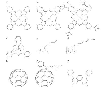
Figure 1.7 Molecular structures of organic semiconducting materials used in OPVs. a) to f) electron donor
materials: a) MPc, b) CuPc, c) TSCuPc, d) SubPc, e) P3HT and f) PTEBS. g) and h) electron acceptor materials: g) C and h) PCBM. i) Exciton blocking material: BCP.
N N
O
OCH3
a) b) c)
d) e) f)
Chapter 1: Introduction
To achieve efficient charge extraction and minimal charge and exciton losses at the electrodes, electrode interlayers based on either TMOs or specific organic molecules are employed. Figure 1.7 introduces the molecular structure of all the organic materials used in further chapters.
1.3.1
Electron donor materials
1.3.1.1 Phthalocyanines
Since their discovery in 1934, phthalocyanines (Pcs) have been used as dyes in inks, and colouring for plastics and clothes (Figure 1.7a-c).[88] More recently interest in this class of molecule has been in their use in organic electronics including organic field-effect transistors (OFET), sensing elements, organic light emitting diodes (OLED) and OPVs, which demonstrates the versatility of Pcs.[26, 89-91]
Pcs are 18 π-electron heteroaromatics, derived from porphyrins, with a large π -system. These macrocycles, also defined as the phthalocyanato anion (C32H16N82-), can act as a metal chelating ligand. The central ligand cavity can accommodate as many as 70 different metal ions and metal oxides (MPc), as well as hydrogen in the simple metal-free type (H2Pc).[92] Pcs prove to be chemically and thermally stable and can be vacuum deposited. In addition to the variety of metal centres, the molecules can be tuned in their solvent solubility as well as electronic and crystalline properties by substitution of the hydrogen groups at the outer ring. Halogenation, for example, shifts the HOMO and LUMO further away from Evac due to the introduction of electron withdrawing groups making it a good electron acceptor.[93] Substitution by ionic sodium sulfonic acid groups (-SO2Na) drastically increases the solubility of otherwise poorly soluble Pcs in water.[94]
Blue coloured CuPc and its derivative, 3,4’,4’’,4’’’-copper(II) phthalocyanine-tetrasulfonic acid tetrasodium salt (TSCuPc), show good absorption in the range 550-700 nm. With a HOMO at -5.1 eV and the LUMO at -3.5 eV they exhibit suitable electron donor properties in combination with fullerenes for OPV devices.[26]
structure shown in Figure 1.8. In this structure the individual molecular stacks are arranged with a well-defined angle to each other. The crystal arrangement and morphology depends greatly on thermal treatment, type of substrate, underlying layer and the nature of any substituents, with bulky substituents leading to larger inter-stack separation.[95, 96] Material properties such as charge mobility and exciton diffusion rely greatly on larger crystalline domains of higher order. In the case of charge mobility Pc
thin films exhibit an anisotropic mobility with enhanced charge transport along the π-π
stacking axis, which influences device behaviour.
Figure 1.8 a) Crystal structure of CuPc in its α-phase. The Cu central atoms are highlighted by the black
markers. b) CuPc crystal alignment on a weakly interacting flat substrate surface.
1.3.1.2 Subphthalocyanines
Subphthalocyanines (SubPcs), a different class of small molecule semiconductor derived from Pcs, were first synthesised in 1972 by Meller and Ossko in an attempt to synthesise boron phthalocyanines.[97] Boron subphthalocyanine consists of only three N-fused diiminoisoindole rings arranged around the central B atom with a substituent, usually a halogen, bound directly to B at the axially accessible top site. The molecule adapts a non-planar, cone-shaped structure with a 14 π-electron system.[98] Compared to Pcs, it was only possible to synthesise boron based subphthalocyanines. SubPcs have two target sites which can be substituted including the organic ligand ring and the open axial site directly bound to the B centre. SubPcs absorb visible light in the range of 500-650
3.4 Å 3.8 Å 24.0 Å
b
b
Chapter 1: Introduction
nm. Unsubstituted boron subphthalocyanine chloride (SubPc – see Figure 1.7d) serves as an electron donor with a LUMO of -3.6 eV and a HOMO of -5.6 eV.[99] If substituted on the ring with appropriate electron withdrawing groups such as halogens, SubPc derivatives can also act as an electron acceptor.[100] The molecular arrangement in a thin film was found to be mainly amorphous due to the non-planar molecular structure and the sterically hindering axial substituent also leading to lower charge mobility compared to planar Pcs.[54, 101] This also leads to pair formation through weak van der Waals interactions rather than efficient π−π stacking.[98]
1.3.1.3 Polythiophenes
Conjugated polymers can undergo an efficient photoinduced charge transfer from the polymer to a fullerene which was discovered in 1992 by Sariciftci et al.[39] Since then the field of semiconducting organic polymers has progressed dramatically with polythiophenes (PTs) and poly(phenylene vinylene) (PPV) being just two well-studied polymer groups out of many with versatile applications not just in OPVs, but also OLEDs, OFETs and other organic electronic applications.[102, 103] Usually, such a polymer chain consists of a huge number of repeat units which create long π-conjugated sequences. The sequences are divided by chain twists and folds which interrupt the
conjugated system. The π-conjugated system is formed by sp2-hybridised carbon atoms and is stretched along the polymer chain. The linear combination of the pz–orbital wavefunctions adds up to an entire band-like π-MO with a broad energy level distribution.[60] To avoid confusion with inorganic bandgap materials it will still be referred to as HOMO and LUMO.
also between chains. For highly regioregular P3HT the hole mobility was greatly improved to 5 x 10⁻²-10-1 cm2V-1s-1.[106] P3HT is very soluble in non-polar or weakly polar solvents such as toluene, chlorobenzene and dichlorobenzene and is mainly deposited as a blend with PCBM to form BHJ active layers, where it undergoes phase separation to form larger polymer domains during film formation. A different derivative is water-soluble sodium poly[2-(3-thienyl)ethoxy-4-butylsulfonate] (PTEBS – see Figure 1.7f) with methoxyalkyl sulfonate side chain group.[107]
1.3.2
Electron acceptor materials
1.3.2.1 Fullerenes
Chapter 1: Introduction
characteristics. Recently, Yang et al. demonstrated the use of organic alternatives to C60 based on F16CuPc.[110]
Delocalisation of π-electrons spread over the molecule surface lead to free rotation within all dimensions without a preferential orientation. Due to weak intermolecular interactions thin films are mainly amorphous with only few crystalline domains. C60 thin films absorb light in two regions of the ultraviolet (UV)/visible (vis) spectrum: There is a broad band in the UV part in the range of 190 to 410 nm and a weak absorption in the visible part around 410 nm to 620 nm due to a forbidden transition.[111, 112] With the HOMO at -6.1 eV and the LUMO at -4.5 eV as well as a high electron
mobility of up to 1 cm2V-1s-1 (OFET) C60 is suitable as an electron acceptor.[113]
Despite its beneficial electronic properties, C60 has a low solubility in most organic solvents and is therefore usually vacuum deposited for small molecule OPV devices. To increase its solubility, C60 was functionalised with a butyric acid methyl ester group, also known as [6,6]-phenyl-C61-butyric acid methyl ester or PCBM (Figure 1.7h). Due to the large increase in solubility, it found application in solution processed polymer/PCBM blend based BHJ OPV devices. In such blends phase separation occurs upon drying and annealing leading to distinct polymer and PCBM domains with a large active D/A interface, crucial for efficient BHJ OPV devices.
1.3.2.2 Transition metal oxides: ZnO and TiOx
TiOx and ZnO can be processed from solution either from nanoparticle suspension or precursor solution. This enables nanostructuring through templating as well as control over crystallinity and morphology to optimise structured D/A interfaces or electrode interlayers. As TiOx is processed from a precursor and then converted to the oxide, the stoichiometry of Ti and O in the nanocrystalline film can vary and a proper TiO2 anatase might not be obtained throughout the entire film.
ZnO is usually an n-type semiconductor due to the presence of defects such as oxygen vacancies and zinc interstitials. ZnO preferentially adopts the wurtzite crystal structure.[115]
1.3.3
Interlayer and electrode materials
1.3.3.1 Charge extraction interlayers
Similar to the electron extraction layers based on TiOx and ZnO, hole extraction interlayers can be employed to optimise the contact at the hole collecting electrode. The quoted VB and CB values for TMOs such as molybdenum oxide (MoOx) and tungsten oxide (WOx) differ by up to a few eV depending on the source and proposed underlying operation mechanism, which shows the need for further investigations. Earlier reports quoted the CB at -2.3 eV and -1.6 eV and the VB at -5.3 eV and -5.1 eV for MoOx and WOx respectively.[120, 121] However, Kroeger et al. reported that MoOx and WOx had large workfunctions and are strongly n-type materials due to oxygen defects. For bulk material the CB was determined to be at -6.7 eV and -6.3 eV, the workfunction at -6.9 eV and -6.5 eV, and the VB at -9.7 eV and -9.7 eV respectively for MoOx and WOx.[122] For TMO thin films of only a few nanometres in thickness, a strong induced dipole at the interface through charge transfer to the electrode results in a huge vacuum level shift. This leads to Fermi level pinning of the n-type TMOs to the electrode material. Additionally, band bending of the adjacent organic material layer towards the TMO occurs up to a few nanometres into the film which is caused by the induced interface dipole.[123, 124]
Chapter 1: Introduction
charge transfer through created defect and gap states.[126] MoOx and WOx are the most frequently employed metal oxide hole extraction interlayers in regular and inverted device architectures.
1.3.3.2 Exciton blocking layer: BCP
Thin films of bathocuproine, 2,9-dimethyl-4,7-diphenyl-1,10-phenantroline (BCP), are almost transparent, and have been deposited on top of the acceptor layer in regular device architectures. The molecular structure is shown in Figure 1.7i. BCP has a large band gap of around 3.5 eV, which leads to the exciton blocking characteristic.[127] Excitons diffusing towards the aluminium electrode cannot travel beyond the acceptor/BCP interface and are not directly quenched at the metal electrode which otherwise leads to a reduction in efficiency.[128] BCP also acts as a sacrificial layer protecting the active organic layer from damage by hot deposited metal from the electrode deposition. Another role of BCP in a device is the built-in-field improvement leading to better diode behaviour of the device.[129] Due to the large bandgap, electron transport through thin layers of BCP is assumed to occur via defect states, which are introduced by metal bombardment during the first few layers of electrode deposition.[130]
1.3.3.3 Electrode materials: ITO and Al
Indium-tin oxide (ITO), the most common transparent conducting oxide (TCO), has most properties of a transparent metal and is widely used as the bottom electrode in OPVs and OLEDs. The high electrical conductivity of the normally insulating indium oxide arises from tin doping.[131]
ITO is sputtered onto glass and can be chemically treated and modified prior to deposition. Due to its relatively high workfunction at around -4.7 eV, it is mainly employed as a hole acceptor from the HOMO of the donor compound, but can collect electrons in inverted device architectures.
functions are magnesium and calcium, but have the disadvantage of high chemical reactivity. Although in inverted devices top electrodes with high workfunctions, such as gold, are required, Al can still be used in combination with metal oxides, such as MoOx and WOx.[125]
1.4
Device interface modification and nanostructuring
Despite great progress in recent years in OPV development, they still perform significantly lower in PCE and operational stability compared to inorganic PV technologies. In order to improve OPVs, crucial interfaces have been identified to have a large influence on device performance, in particular the D/A and electrode/photoactive layer interfaces. The interface structure and choice of material at these interfaces is critical.[84, 85, 132-134] By developing new methods based on controlled nanoengineering to structure and optimise these interfaces, deeper understanding can be gained and device improvement can be achieved.
As shown in the principle of operation of a D/A heterojunction OPV device, the conversion efficiency of solar energy into electrical energy is greatly dependant on the four individual processes determining EQE and therefore JSC. Different approaches are presented to contribute to a solution for improved OPV device performance: D/A interface nanostructuring, electrode contact interface modification by inserting TMO interlayers, and organic/inorganic D/A hybrid OPVs as an alternative approach to fullerene based acceptor materials.
1.4.1
D/A interface modification
1.4.1.1 Background and development of interface nanostructuring
Chapter 1: Introduction
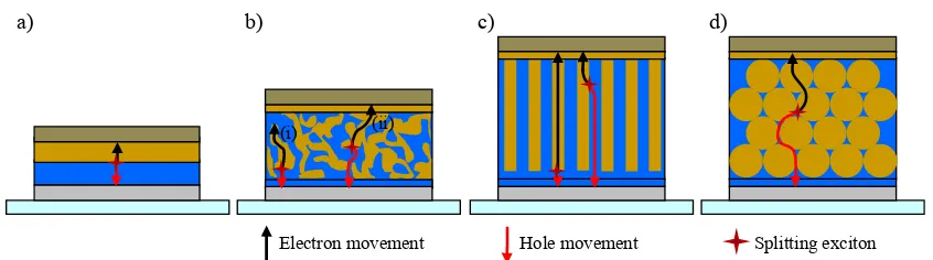
[image:42.595.88.511.208.326.2]Therefore a compromise between the film thickness for maximum absorbance and the limited LD for efficient exciton dissociation is essential for efficient photocurrent generation. This relationship defines the main limiting factor of planar bilayer OPV devices as shown in Figure 1.9a.[26]
Figure 1.9 Schematic of different heterojunction OPV device architectures: a) bilayer, b) BHJ or mixed
layer, c) and d) 3D nanocomposite devices. The black and red arrows indicate the traveling path of electrons and holes respectively. In b) (i) is a situation of a charge trapped in a dead end and (ii) shows successful charge transport to the collecting electrodes after exciton splitting.
To minimise the exciton diffusion paths and to generate a larger interface with increased total active layer thickness, D/A intermixed active layers were introduced, including solution-processed polymer/fullerene BHJ devices and vacuum co-deposited small molecules. In both cases charge transport pathways towards the charge collecting electrodes through randomly mixed layers are limited due to numerous isolated domains and cul-de-sacs in the D/A layer system resulting in charge trapping and recombination, as highlighted in Figure 1.9b. Despite the current density increase in both BHJ and mixed layer structures, there is an unavoidable trade-off between the improved ηedand reduced ηcc.[26, 135] By optimising the deposition conditions and by applying post-treatments such as temperature and solvent annealing a certain control over phase segregation and therefore the D/A interface order can be achieved.[136, 137] A theoretical study by Yang et al. on photo-current generation in nanostructured OPVs revealed exactly the same trend. As the domain size of a D/A mixed layer was increased the specific interface area in a defined unit cell dropped resulting in an improved ηcc but reduced ηed and a small, but still noticeable improvement in internal quantum efficiency (IQE).[132]
Splitting exciton Hole movement
Electron movement
(i) (ii)
To overcome this problem a more controlled three-dimensional (3D) highly interpenetrating D-A composite structure is required to exploit the advantages from BHJ and mixed layers, but with well structured charge transport paths.
Potential solutions for this complex problem are ordered organic nanostructures which would result in an increase in interface area, and therefore short exciton diffusion pathways, but also continuous charge transport pathways with increased film thickness and therefore improved absorbance.
An ideal solution is a finger-shaped interdigitated D-A device architecture with a small diameter to meet the LD criterium.[138, 139] Such structures have been realised in hybrid devices from vertically aligned metal oxide nanorods, but the devices showed only slight device current improvement.[140-142] Another promising attempt by Haberkorn et. al. is the template-assisted fabrication of free-standing nanorod arrays of a hole-conducting crosslinked triphenylamine derivative.[143] A new route to achieve such ordered D/A interface patterning on a length scale of a few tens of nanometres in domain size is the use of self-assembled block copolymers facilitating donor and acceptor domains in the same chain. This route is complex from a synthetic and self-assembly point of view and remains very challenging.[144] However, such a finger-shaped interpenetrating D/A system is not easy to realise on a sub-100 nm scale for purely organic OPVs (Figure 1.9c).
Close approximations to interpenetrating nanostructured interfaces have been produced by nanosphere lithography (NSL).[145] NSL has been used to generate nanosphere templated 2D nanocomposite organic thin film structures based on a nanoparticle monolayer mask as a template, which consists of 2D-ordered nanosphere arrays. However, the interface area would be greatly compromised compared to any mixed or BHJ interface.
Chapter 1: Introduction
fabrication process of 3DOM thin films typically involves three separate steps: (i) self-assembly of colloidal spheres or droplets into supra-structures; (ii) infiltration of the interstitial spaces with an application-specific material; and (iii) template removal. In certain cases the first two steps are combined into a single co-deposition procedure. The nanosphere templating process is widely applicable to inorganic materials including metal oxides and metals but proves to be very challenging for organic semiconductors.[146] Further details are revealed in Chapter 5.
1.4.1.2 Concept and fabrication strategies
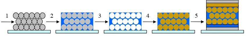
3D nanosphere templating involves numerous steps and processes to obtain the highly interpenetrating D/A composite structure: 1) convective self-assembly of polystyrene colloids to form the template structure, 2) infiltration of the nanosphere domains with appropriate donor material, which can be combined to a direct co-deposition, 3) colloid removal step, 4) second infiltration of the inverse structure with acceptor material, and 5) deposition of buffer layer and vacuum deposition of the covering top electrodes. The schematic of nanosphere templating for a complete nanocomposite device is shown in Figure 1.10.
Figure 1.10 Schematic of fabrication method: 1) Self-assembly of polystyrene colloids, 2) infiltration of
nanosphere domains with appropriate donor material, 3) colloid removal, 4) infiltration of inverse structure with acceptor material, 5) device fabrication using 3D nanosphere templating combined with organic molecular beam deposition. 1) and 2) can be combined to a co-deposition step.
In this unique approach to template organic semiconducting materials the templating material is sacrificial, which explains the choice of polystyrene (PS). The system is based on a two-phase system starting with water as a solvent and dispersion medium for PS and the water-soluble donor materials (PTEBS and TSCuPc). The removal process of the PS template by using non-polar solvents is selective leaving the
2 3 5
[image:44.595.88.511.478.541.2]inverse opal structure made of donor material unchanged. The second infiltration of the acceptor material has to be performed from a non-polar solvent to prevent the remaining structure from damage or even complete dissolution. In this delicate approach it is of great importance to create a clean D/A interface avoiding any residues from the performed process steps and more importantly from the template. PS is a very good insulator and a thin film could already ruin the device without being detected. Other sources of residues are soaps which are added to stabilise the nanospheres during and after synthesis. Soaps and other additives are also the reason why all nanospheres were synthesised in house to control all parameters and compounds involved in the synthesis.
Co-deposition was developed to target very small sphere sizes down to 50 nm in diameter in order to match LD, and is completely new to the field. The templating approach can also be used to template TiOx and ZnO for nanostructured electrodes or hybrid devices.
1.4.2
TMO interlayers
Ideally, the photoactive layer consisting of donor and acceptor materials is sandwiched between two appropriate ohmic contacts to avoid any energetic barrier for efficient charge extraction. Enhanced selective charge extraction can be achieved by introducing TMOs between electrodes and the photoactive layer. Also the device stability can be improved by metal oxide encapsulation.[84, 85]
Chapter 1: Introduction
Metal carbonates and TMOs including cesium carbonate (Cs2CO3), but mainly TiOx and ZnO, work as electron extraction layers on the opposite electrode side following the same concept.[104, 118, 119] For electron conducting materials such as PCBM a very close energy level alignment between the TMO CB and the PCBM LUMO can be achieved forming an ohmic-like contact.[85] TiOx and ZnO are both n-type materials, transparent in the visible range and are not limited to thin layers due to their exceptionally high electron mobility. Solution processing of TMOs enables nanostructuring through templating, thicker spacer layers for improved optical interference, as well as generally good control over crystallinity and morphology to optimise structured D/A interfaces or electrode interlayers (see Chapter 2).[149, 150]
Hole and electron extracting TMO interlayers also have the general effect of improving the homogeneity of conductivity and workfunction. Additionally, when employed on one electrode or even as a sandwich structure from both sides operational device stability is greatly improved by preventing direct electrode contact which can lead to chemical and physical reactions.[85, 124]
Investigations into different thin film structures from selected deposition methods of ZnO, such as spray pyrolysis and controlled electrodeposition are the target of the investigation in this thesis. The focus is on the ITO/TMO interface as well as the TMO/blend interface. TiOx from sol-gel process are also employed to compare the systems. This should serve to develop a deeper understanding of the structure/function relationship between film morphology, crystallinity and device performance but also to optimise OPV device performance. In order to be able to compare the different systems to each other, and also work in the literature, the well known D/A BHJ system based on P3HT/PCBM was chosen.
1.4.3
Hybrid OPVs
Fullerene replacement by inorganic semiconductors such as TiOx and ZnO with high electron mobility and potential for nanostructuring demonstrates a promising concept for hybrid OPVs.[117, 151, 152] Organic/inorganic hybrids have the advantage of combining highly absorbing organic donor materials with chemically and thermally stable, robust and cheap inorganic electron acceptor materials to produce thin film hybrid OPV devices. TMOs also provide a controlled interface with suitable energy levels to act as an electron acceptor with appropriate donor materials.
TiOx and occasionally ZnO are employed in DSSCs.[152] In contrast to DSSCs, D/A heterojunction hybrid OPVs employ the organic donor material not just as a sensitiser but also as charge transport material. Hybrid devices are much thinner than DSSCs, not exceeding 100 nm.
ZnO and TiOx have a favourable energy band alignment with commonly used polymeric organic donor materials such as P3HT and poly(2-methoxy-5-(2’-ethyl-hexyloxy)-p-phenylene vinylene) (MEH-PPV). For both planar bilayer and nanostructured hybrid TMO/polymer devices, PCE is primarily limited by the low JSC due to poor photocurrent generation with the vast majority of reported devices not exceeding a PCE of 0.5 %.[153, 154] Due to the variety of processes from solution which can be used to deposit TMOs, surface nanostructuring through specific growth or templating is favourable. A lot of work has been carried out on the formation and implementation of TMO nanorods and other surface area increasing “pseudo 2D” structures. Most structures were implemented in polymer hybrids showing an increase in performance mainly due to a higher JSC based on the larger active surface area.[140, 142] The best devices with a PCE of up to 2 % are P3HT/ZnO nanoparticle blends forming BHJ-like interconnected photoactive layers.[155] More efficient polymer hybrid devices of up to 2.8 % are based on semiconductors including cadmium sulphide (CdS), cadmium selenide (CdSe) and copper indium selenide (CuInSe2) which contribute significantly to
![Figure 1.1 Development of PV devices including OPVs quoting the efficiencies for different technologies from1976 until 2010.[9]](https://thumb-us.123doks.com/thumbv2/123dok_us/9684483.469926/19.595.88.517.386.679/figure-development-devices-including-quoting-efficiencies-different-technologies.webp)
![Figure 1.5 a) Binding energy diagram of a typical organic (comparing the Bohr radius ε=4) and inorganic (ε=15) semiconductor rB and Coulomb radius rC (adapted from Hanna et al.).[61] The three different types of excitons include b) Mott-Wannier, c) charge-](https://thumb-us.123doks.com/thumbv2/123dok_us/9684483.469926/29.595.91.508.93.306/binding-comparing-inorganic-semiconductor-coulomb-different-excitons-wannier.webp)