Abstract—As Moore’s law continues, the number of cores on a chip in Chip-Multiprocessors (CMPs) has been increasing. As the number of cores increases, more cache resources are needed, and as a result, the leakage power consumption of the cache accounts for a larger proportion of the total chip power consumption. The emerging non-volatile memory (NVM) is expected to replace traditional memory devices due to its high density, near zero leakage power, and non-volatile memory. In this paper, we use STT-RAM, a most promising candidate of NVM, in the cache architecture. We proposes a hybrid cache spherical placement scheme for 3D CMP, which reduces power consumption by 34.94% and performance by only 1.49%
degradation compared to a CMP architecture that uses SRAM as cache with the same capacity. Based on this hybrid cache architecture, this paper further studies the problem of hybrid cache data migration in 3D CMP and proposes a hybrid multicore cache dynamic migration scheme. This scheme reduces the data migration jitter of 3D CMP by recording the previous migration information of data and restricting the data migration from SRAM to STT-RAM, and solves the problem of data migration failure of hybrid cache.
Index Terms—CMP, NVM, Hybrid Cache, Data Migration
1I. INTRODUCTION
hip Multiprocessor (CMP) has become the effective architecture for modern and future multicore processors.
As Moore's law continues, the number of cores in CMP is increasing rapidly every generation. As the number of cores increases, more cache resources are needed to feed all the cores. The three-dimensional integrated circuits (3D ICs) technology, where multiple cache layers are stacked vertically, has been proved to be a promising solution to increase the cache resources on a chip [1-4]. Because the 3D ICs design can mitigate the large off-chip memory access latency and
Manuscript received March 6, 2018.This work was supported in part by the Natural Science Foundation of China under Grant 61774086 and 61701228, the Natural Science Foundation of Jiangsu Province under Grant BK20160806, and the Fundamental Research Funds for the Central Universities under grant NS2016041 and NS2017023.
Lei Wang, the College of Electronic and Information Engineering, Nanjing University of Aeronautics and Astronautics(NUAA), Nanjing 210016, China (email: [email protected])
Fen Ge, the College of Electronic and Information Engineering, Nanjing University of Aeronautics and Astronautics(NUAA), Nanjing 210016, China (email: [email protected])
Hao Lu, the College of Electronic and Information Engineering, Nanjing University of Aeronautics and Astronautics(NUAA), Nanjing 210016, China (email: [email protected])
Ning Wu, Ying Zhang, and Fang Zhou, are the College of Electronic and Information Engineering, Nanjing University of Aeronautics and Astronautics(NUAA), Nanjing 210016, China (email: [email protected], [email protected], [email protected])
bandwidth constraints. The CMP that uses 3D ICs design is called 3D CMP. However, cache architecture is one of the most power-hungry parts of the 3D CMP, because the leakage power in cache systems has become an import contributor in the overall chip power consumption. Therefore, it is very necessary to reduce the power consumption generated by the cache architecture. The emerging non-volatile memories (NVM) have potential application in the memory architecture to reduce the leakage power consumption due to their benefits such as high storage density and near zero leakage power consumption. Spin-transfer torque random access memory (STT-RAM) is the most promising candidate of NVM, because it combines the access speed of SRAM, high density and non-volatile characteristics of DRAM. Although STT-RAM has so many advantages, it has large write latency and write power consumption, which restricts it to directly replace traditional memory devices. In order to overcome these disadvantages of STT-RAM, a hybrid cache architecture is adopted. In the hybrid cache architecture, the ratio of SRAM to STT-RAM and their placement affect the power consumption in cache architecture. Besides, the data migration scheme between SRAM and STT-RAM has significant effects in the dynamic power consumption.
Therefore, in the hybrid cache architecture, the optimal placement of STT-RAM and SRAM and the migration scheme are worth researching problems.
A number of recent studies have addressed the problem of hybrid architecture design in CMP[5-9]. Lin [5] uses hybrid cache partitioning to improve write operations in Non-Uniform Cache Architecture (NUCA) architectures.
They classify the L2 cache into four regions, one for SRAM Bank and three for STT-RAM Bank, based on the number of write operations and the way each processor accesses for SRAM and STT-RAM. However, they do not consider the hybrid cache partitioning in 3D CMP. Chen [6] proposes a dynamically reconfigurable hybrid cache architecture for the last-level cache of processors. In this architecture, hit counters are added in the cache structure to dynamically adjust the ratio of NVM and SRAM. However, the proposed dynamically configurable hybrid cache architecture may result in data migration jitter. Ahn [7] introduces the concept of write-intensity prediction to optimize the hybrid cache architecture. The processor has a high probability of frequent write operations on the cache when running. Following these instructions, it is possible to predict which of the cache banks have greater write intensity in the next operation. In their study, the decision threshold for the cache bank that is most
A Spherical Placement and Migration Scheme for a STT-RAM Based Hybrid Cache in 3D chip
Multi-processors
Lei Wang, Fen Ge, Hao Lu, Ning Wu, Ying Zhang, and Fang Zhou
C
likely to perform data migration is difficult to determine. Low thresholds increase the chance of unnecessary migration, and high thresholds reduce the significance of migration.
Based on the problems presented above, this paper studies hybrid cache architecture in 3D CMP based on STT-RAM and proposes a hybrid cache spherical placement and an optimized hybrid cache dynamic migration scheme to minimize the power consumption generated by the hybrid cache architecture and data migration. The rest of the paper is organized as follows: Section II presents the hybrid cache placement approach of 3D CMP. Section III describes the hybrid cache dynamic migration scheme. Experimental results are demonstrated in section IV and we finally conclude our work in section V.
II. THE SPHERICAL PLACEMENT APPROACH A. 3D CMP Architecture
In 3D CMP architecture, the processor layer is generally placed near the heat sink, on the bottom of the chip [10-11].
The processor core has private L1 cache, which consists of instruction cache and data cache. The cores are connected via network-on-chip (NoC). Above the processor layer, multiple level caches are stacked. As shown in Figure 1, two layers of level 2 cache are stacked. Each cache layer has 16 cache banks, which are connected via NoC. Different layers are connected by through silicon vias (TSVs).
Core node L2 SRAM Cache Router
L2 Cache
L2 STT-RAM Cache
Fig.1 3D CMP hybrid cache architecture
The NUCA is commonly adopted in 3D CMP. In NUCA, for a given core, the access to closer cache banks is much faster compared to the farther banks. NUCA can be divided into two categories: static NUCA (S-NUCA) and dynamic NUCA (D-NUCA). For S-NUCA, a given physical address will be mapped to a single cache bank. As for D-NUCA, each physical address can be mapped to a set of cache banks to allow flexible block placement. Using D-NUCA in CMP, the access to the cache is not uniform. Most of the access operations occur on a small portion of the bank in the central of the cache layer [12].
B. Hybrid Cache Spherical Placement Approach
According to the cache access characteristics of D-NUCA mentioned above, we propose a hybrid cache spherical placement approach for 3D CMP. As shown in Figure 2, we take two 4×4 cache layers as an example to calculate the average access distance of each cache bank in a 3D CMP architecture. The average access distance for a cache bank is calculated by the average route hops from each processor core to this cache bank. It is found that cache banks with short access distances are distributed in the central area of this
cache layer, the cache banks with large access distance are distributed in the edge of this cache layer. And in different cache layer, the average access distance is different. The average access distance in the bottom layer tends to be smaller than that in the top layer, because the bottom layer is near the processor layer. Therefore, the spatial distribution of cache banks with different access layers tends to be hemispherical.
Based on the relation between average access distance and placement, we propose a hybrid cache spherical placement approach.
2.7 3.2 2.7 3.2
2.1 2.7 2.1 2.7
2.1 2.7 2.1 2.7
2.7 3.2 2.7 3.2
3.7 4.2 3.7 4.2
3.1 3.7 3.1 3.7
3.1 3.7 3.1 3.7
3.7 4.2 3.7 4.2
Fig.2 3D CMP cache bank average access distance
The spherical placement approach is described as follows.
In a cache layer, the cache banks with short average access distance preferably use SRAM, and that with large average access distance use STT-RAM. The cache banks with short average access distance are distributed in the central of the cache layer. Therefore, the SRAM cache banks in a cache layer are distributed like a circle, and the radius of the circle is related to the distance between the cache layer and the processor layer. For the cache layer near the processor layer, the average access distance of the cache banks is smaller, so the radius of the SRAM distributed circle is large. As for the cache layer far away from the processor layer, the radius of the circle is small. In general, the spatial distribution of SRAM cache banks tend to be one hemisphere.
III. HYBRID CACHE DYNAMIC MIGRATION SCHEME OF 3D CMP
In the 3D CMP with our proposed spherical placement of hybrid cache, the traditional NUCA may cause data migration problems presented as follows..
A. Problems with data migration 1) Data migration jitter
In 3D CMP, different cores accessing the same cache line
may generate two requests in two opposite direction for data
migration. Figure 4 shows the jitter problem with 3D CMP
data migration. As shown in the figure, core 3 and core 15
share a cache line in bank 7. At time T1, the access frequency
of core 15 to the shared cache line reaches the threshold of
data migration, and according to the traditional data migration
scheme, the shared cache line will be migrated from bank 7 to
bank 11. At time T2, the access frequency of core 3 to the
shared cache line also meets the data migration condition, and
the shared cache line is relocated from bank 11 to bank 7. If
both core 3 and core 15 have frequent access to the shared
cache line for a certain amount of time, the shared cache lines
will migrate between bank 11 and bank 7 frequently. This
frequent migration phenomenon of a cache line in the two
opposite directions between the banks, called the data
migration jitter.
Fig.4 CMP data migration jitter
For the entire CMP, when data migration jitter occurs, the data migration will not reduce the average data access latency, and itself will produce additional power consumption overhead. Frequent data migration increases the amount of data on the on-chip network, so data migration jitter problems have a negative impact on the power and performance of CMP.
The problem of data migration jitter is mainly due to frequent data migration in two opposite directions. Therefore, increasing the threshold of data migration may reduce the frequency of data migration. However, simply increasing the threshold of data migration will weaken the effect of data migration on system performance. Therefore, how to reduce the frequency of data migration in two opposite directions while ensuring normal data migration is important in solving the data migration jitter problem.
2) Hybrid cache data migration failure
In hybrid cache architectures, the latency of data access depends on the physical distance between the processor core and the cache bank holding the data, and the type of cache bank holding the data. For example, in our proposed architecture, if data migrates from STT-RAM to SRAM, the average access distance and write latency will both be reduced. However, when migrating data originally stored in the SRAM to the STT-RAM, the write latency will increase even though the average access distance is reduced.
In the 2GHz system, the latency caused by the routing of the on-chip network is about 2 clock cycles. The read latency of SRAM and STT-RAM is about 6 clock cycles. The write latency of STT-RAM is more about 36 clock cycles. When data migrates from SRAM to STT-RAM, the average access distance is shorted, but the write latency of 30 clock cycles is caused. Therefore, in this case the data migration of the hybrid cache architecture loses its significance.
Due to the data migration from SRAM to STT-RAM, the traditional data migration scheme in hybrid cache architecture can not result in the expected improvement in system performance.
B. Hybrid Cache Data Migration Scheme
Based on the above mentioned problems, we propose an optimized scheme for data migration in 3D CMP hybrid cache architecture.
The scheme proposed in this paper assumed that the priority of data migration in different directions is: X
direction> Y direction> Z direction. If the data migration priority in the Z direction is set to high, all the data that needs to be migrated will be migrated to the cache layer at the bottom layer near the processor layer. Thus, the data transmission in the Z direction will become crowded. Besides, the data in the bottom cache layer is often the most frequently accessed data, and replacing the data in the bottom layer will make the cache performance decreased.
In addition, the migration of data from SRAM to STT-RAM is forbidden. Based on the hybrid cache spherical placement proposed in this paper, the STT-RAMs are located at the edge of the cache layer and are spatially distributed outside the SRAM. If data migrates from SRAM to STT-RAM, it is likely to increase the average access distance of the cache bank.
In order to realize the proposed data migration scheme, we modify the traditional structure of the cache line. As shown in Figure 5, each cache line added the X and Y two bit to preserve the previous migration information. The X flag bit is used to record the data migration in the west and east directions, and the Y flag bit is used to record the data migration in the north and south directions. If X is a ‘0’ , it means that data has not been migrated in the west and east directions or has been migrated to the west direction in the existing cache bank. If X is a ‘1’, it means that data has been migrated to the existing cache bank in east direction. If Y is a
‘0’, it indicates that data has not been migrated to north and south migration or data has been migrated to the north direction in the existing cache bank. And if Y is a ‘1’, it indicates that the data has been migrated in the south direction to the existing cache bank.
tag X Y data
Fig.5 Modified cache line structure
In the proposed hybrid cache data migration scheme, when the cache line receives the migration request, it judges the state of the last data migration. If the migration request is in the same direction as the last migration, then the data migrates.
If the direction of the migration request is different from the direction of the last data migration, the corresponding flag bit is modified but the current data migration is refused. We take the data migration between west and east direction request as an example. If the cache line receives a data migration request from the west direction, it will judge the state of the flag bit X at this moment. If the value of X is a ‘0’ at this moment, the data migration is allowed directly. If the value of X is a ‘1’ at this time, the value of X is rewritten to a ‘0’, but no data migration is performed.
IV. EXPERIMENTAL RESULT
In this section, we present the evaluation of the proposed hybrid cache spherical placement and data migration scheme.
First, the evaluation methodology is illustrated. Second, we present the experimental results and the analysis.
A. Experiment Setup
In this paper, a gem5-based simulation platform is used.
Experiments are conducted using the Spec2006 standard test
assembly to obtain the simulation results of the power consumption and performance of the 3D CMP, using the hybrid cache data migration scheme proposed in this paper, and compared with the experimental results of the traditional data migration scheme. Table I describes the main simulation parameters.
TABLE II Simulation Parameters
Core 16 nuclear out of order execution processor, 2GHz, ALPHA ,4 × 4 Mesh
L1 Caches
Private, instruction and data cache, each cache is 32KB.2-way associative, 64 B block, LRU
replacement, 2-cycle latency
L2 Cache
Shared, 16-way, 64 B block, LRU replacement, 6-cycle latency for SRAM,36-cycle latency for
STT-RAM Cache
Coherence Protocol
MESI
Main
Memory 4G, 300-cycle latency
We model a 16-core 3D CMP system with two-level on-chip cache hierarchy similar to Fig.1. Each core has private L1 instruction and data caches. The capacity of L1 cache is 16×32KB SRAM.
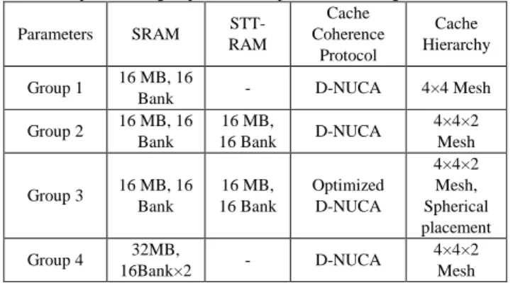
We compare the proposed hybrid cache spherical placement and data migration scheme with three experimental groups as shown in Table III. The experimental group 1 and the experimental group 4 both use SRAM as the L2 cache, but the capacity of the cache is different. In the experimental group 1, one layer of 16MB cache layer is stacked on the processor layer, and the experimental group 4 is stacked two 16MB cache layer. The experimental group1 and 4 are compared to evaluate the impact of different cache capacity on the system power consumption and performance. L2 cache in experimental group 2 is a hybrid structure of SRAM and STT-RAM, in which SRAM is located on one layer and STT-RAM is located on the other layer. Experimental group 3 uses the proposed hybrid cache spherical placement and the optimized data migration scheme. Experimental group 2 and 3 are compared to evaluate the impact of different hybrid cache architectures and data migration schemes on the system power consumption and performance.
We use a set of SPEC2006 benchmarks for multi-programmed workloads. The SPEC2006 benchmarks are classified into four categories, as shown in Table IV.
TABLE V
Experimental group simulation parameters configuration
Parameters SRAM STT- RAM
Cache Coherence
Protocol
Cache Hierarchy
Group 1 16 MB, 16
Bank - D-NUCA 4×4 Mesh
Group 2 16 MB, 16 Bank
16 MB,
16 Bank D-NUCA 4×4×2
Mesh
Group 3 16 MB, 16 Bank
16 MB, 16 Bank
Optimized D-NUCA
4×4×2 Mesh, Spherical placement Group 4 32MB,
16Bank×2 - D-NUCA 4×4×2
Mesh
TABLE VI Simulation Parameters
Application Read operation ratio Write operation ratio
bzip2 86.2% 13.8%
libquantum 100% 0%
hmmer 63.6% 36.4%
lbm 15.7% 84.3%
mcf 94.5% 5.5%
B. Result Analysis
Figure 6 shows a comparison of the normalized system performance. The performance is measured by the parameter IPC. The experimental group 3 on average achieves 11.12%
performance improvements than that of experimental group 1, 2.38% improvements than that of experimental group 2 and 1.49% degradation than that of experimental group 4. For compute-intensive applications such as bzip2 and hmmer, the performance of the system is mainly due to the speed of the processor, so increasing the capacity of the cache does not significantly improve the system performance. While the libquantum and lbm two programs are cache-intensive applications, the program will produce a large number of read and write operations, and the increase in cache capacity will reduce the data access latency. Therefore, with the benchmark libquantum and lbm, the system performance is greatly improved.
Fig.6.Normalized system performance
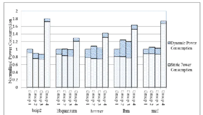
Figure 7 shows the normalized system power consumption
comparison. The leakage power consumption of experimental
group 2 and the experimental group 3 is relatively low,
because these two experimental groups all use STT-RAM as
cache. When running two cache-intensive programs of hmmer
and lbm frequently, the dynamic power consumption of the
overall power consumption is increasing due to the high write
power consumption of STT-RAM. The experimental group 3
on average increases 2.53% power consumption than that of
experimental group 1, but achieves 2.77% energy saving than
that of experimental group 2, and 34.94% energy saving than
that of experimental group 4.
Fig.7.Normalized system power consumption
Figure 8 shows the system performance-power consumption ratio of different experimental groups. By the analysis of system performance-power ratio, we can evaluate the performance gains with increasing the power consumption of the different cache architectures. The experimental results show that the system using our proposed hybrid cache architecture has shown a better performance-power consumption ratio in most cases.
Fig.8 System performance- power consumption ratio
V. CONCLUSION
In this paper, we proposed a spherical placement and data migration scheme for STT-RAM based hybrid cache in 3D CMP. The experiments carried out with SPEC2006 benchmarks show that the proposed spherical placement and data migration scheme can achieve 34.94% energy saving on average with 1.49% performance degradation, compared with the architecture which uses pure SRAM as the cache in the same capacity.
R EFERENCES
[1] Haensch W. Why should we do 3D integration?[C]// Design Automation Conference, 2008. DAC 2008. ACM/IEEE. IEEE, 2008:674-675.
[2] Xie Y, Loh G H, Black B, et al. Design space exploration for 3D architectures[J]. Acm Journal on Emerging Technologies in Computing Systems, 2006, 2(2):65-103.
[3] Loh G H, Xie Y. 3D Stacked Microprocessor: Are We There Yet?[J].
IEEE Micro, 2010, 30(3):60-64.
[4] Chen K N, Tan C S. Integration schemes and enabling technologies for three-dimensional integrated circuits[J]. Computers & Digital Techniques Iet, 2011, 5(3):160-168.
[5] C. Lin, J.-N. Chiou, "High-Endurance Hybrid Cache Design in CMP Architecture With Cache Partitioning and Access-Aware Policies", IEEE Transactions on Very Large Scale Integration (VLSI) Systems, vol. 23, pp. 2149-2161, 2015.
[6] Chen Yuting, Cong Jason, Huang Hui, et al. Dynamically reconfigurable hybrid cache: An energy-efficient last level cache design [C] // Proc of the Conf on Design, Automation and Test in Europe, Piscataway, NJ: IEEE, 2012:12-16.
[7] Ahn J, Yoo S, Choi K. Write intensity prediction for energy-efficient non-volatile caches [C] //Proc of 2013 IEEE Int Symp on Low Power
Electronics and Design (ISLPED), Piscataway, NJ; IEEE, 2013:
223-228
[8] Q. Li, J. Li, L. Shi, M. Zhao, C. J. Xue, Y. He, Compiler-assisted STTRAM-based hybrid cache for energy efficient embedded systems.
IEEE
Transactions on Very Large Scale Integration (VLSI) Systems, vol.22, 2014, pp. 829-1840.
[9] R. J. Behrouz and H. Homayoun, NVP: Non-uniform Voltage and Pulse
width Settings for Power Efficient Hybrid STT-RAM, IEEE international
Green Computing Conference, 2014, pp. 1 – 6.
[10] Zhou X, Xu Y, Du Y, et al. Thermal Management for 3D Processors via Task Scheduling[C]// International Conference on Parallel Processing. IEEE, 2008:115-122.
[11] Wang H, Fu Y, Liu T, et al. Thermal management via task scheduling for 3D NoC based multi-processor[C]// Soc Design Conference. IEEE, 2010:440-444.
[12] Beckmann B M, Wood D A. Managing Wire Delay in Large
Chip-Multiprocessor Caches[C]// International Symposium on
Microarchitecture. IEEE, 2004:319-330.