Simulation of Transmission Electron Microscope Images
of Dislocations Pinned by Obstacles
Yuhki Satoh
+1, Takahiro Hatano
+2, Nobuyasu Nita
+3, Kimihiro Nogiwa
+4and Hideki Matsui
+5Institute for Materials Research, Tohoku University, Sendai 980-8577, Japan
From a direct observation of dislocation-obstacle interaction utilizingin situstraining experiments in transmission electron microscope (TEM), the obstacle strength factor could be evaluated from pinning angles of dislocation cusps. We simulated this process: we produced a dislocation cusp by molecular dynamics simulation of interaction between an edge dislocation and a void or a hard precipitate in copper, and calculated the TEM image by multislice method. In two-beam conditions, cusp images showed inside-outside contrast depending on the sign of the diffracting vector and other variations with the specimen geometry. The pinning angles measured on TEM images ranged up to a few tens of degrees and were between the true angles for the two partial dislocations. Characteristics and contrast mechanisms of cusp images were discussed based on those of dislocation dipoles. [doi:10.2320/matertrans.MD201312]
(Received September 3, 2013; Accepted October 2, 2013; Published November 15, 2013)
Keywords: transmission electron microscope, image simulation, dislocation-obstacle interaction, irradiation hardening
1. Introduction
Various crystal lattice defects induced by neutron irradi-ation, such as precipitates, voids, dislocation lines and loops are responsible for degradation in mechanical properties: increase in yield stress, loss of ductility, and increase in ductile-brittle transition temperature. A number of researches have been devoted for defect structural evolution and mechanical property changes under neutron irradiation for nuclear materials development. Understanding the mecha-nisms involved is necessary to construct models for estimating the lifetime of components of nuclear power plant. In an elementary process of dislocation-obstacle interac-tion, a gliding dislocation is pinned by obstacles and bows out to form arcs between the neighboring pinning points, which induces cusps on the dislocation at obstacles. The apex angle of the dislocation cusp is referred to as the pinning angleº. The dislocation breaks away by bypassing or cutting through the obstacle when the pinning angle reaches a critical value ºc. Stronger obstacles have smaller critical angles. The obstacle strength factor¡¼cosðºc=2Þand the distance between the neighboring pinning points are the key parame-ters that relate the defect microstructure to the change in macroscopic mechanical properties. There have been re-ported a few attempts to evaluate the factor from a direct observation of dislocation-obstacle interaction utilizing
in situstraining experiments in transmission electron
micro-scope (TEM).13) The method has not been widely applied so far, due to high technical levels required for in situ experiments. Another difficulty comes from TEM images with a limited resolution both in time and space for measuring pinning angles of radiation-induced obstacles,
typically less than a few nanometers in size, at a moment of the breakaway. Alternatively, molecular dynamics (MD) simulations have been applied extensively for the dislocation-obstacle interaction.47)
In the present study, we performed TEM image simulation of dislocation cusps to examine whether TEM images reveal the cusp structure in the scale suitable for evaluating the obstacle strength factor. For this purpose, we stopped MD simulation of interaction between an obstacle and an edge dislocation just before the breakaway. We then calculated TEM images of dislocation cusps under various conditions using the multislice method. We compared apex angles between the cusp structure and on the calculated images, which would support the experimental evaluation of the obstacle strength factor.
2. Calculation Procedure
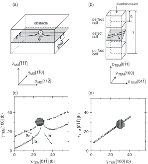
The axes of the MD calculation cell were taken along xMD½112, yMD½110 and zMD½111, respectively. A typical cell had the dimensions of 23, 23 and 15 nm, and contained approximately 5.5©105 copper atoms of fcc structure (a=0.3615 nm). It employed the interatomic potential given by Acklandet al.8)We introduced a spherical void (radius 1, 2 or 3 nm) or a hard precipitate (radius 1.5 nm) as an obstacle. The hard precipitate was modeled by a group of immobile atoms that were coherent with the matrix crystal.7) We induced also a perfect edge dislocation with Burgers vector
b¼a=2½110, and it dissociated into two Shockley partial dislocations b1¼a=6½211 (leading partial) and b2¼ a=6½121 (trailing partial). The glide plane bounded by the two partials involved a stacking fault with the displacement vector R=¹a/3[111]. The geometry of the cell was schematically shown in Fig. 1(a). Periodic boundary con-dition was applied in xMD and yMD directions. In MD calculation at 300 K, the dislocations were driven toward
¹yMD direction at a strain rate of 8©106s¹1; the lower (¹zMD) surface was moved along ¹yMDdirection while the upper surface wasfixed. The model supposed the two partial dislocations of infinite length inxMDdirection to glide along
+1Corresponding author, E-mail: ysatoh@imr.tohoku.ac.jp
+2Present address: Earthquake Research Institute, The University of Tokyo,
Tokyo 113-0032, Japan
+3Present address: Central Research Institute, Mitsubishi Materials
Corporation, Naka, Ibaraki 311-0102, Japan
+4Present address: Japan Atomic Energy Agency, Tsuruga 914-8585, Japan
+5Present address: Institute of Advanced Energy, Kyoto University, Uji
611-0011, Japan
Special Issue onIn SituTEM Observation of High Energy Beam Irradiation
¹yMD direction under shear strain, and to interact with periodically arranged obstacles in a thin film. See Refs. 5) and 6) for the method and results of the MD simulation; we do not go into further details.
The MD calculation was stopped just before the leading partial broke away from the obstacle, and each atom was relaxed to the equilibrium position by a static method. Then the defect cell that contained the obstacle and the dislocation cusp was cut from the MD cell. The cell was sandwiched between two perfect lattices in the TEM image simulation system, as is schematically shown in Fig. 1(b). The size of the defect cell was 14.3 nm (56b), 14.5 nm (40a), 14.1 nm (55b), along xTEM½011, yTEM½100 and zTEM½011 axes, respectively, where b denotes the atomic distance (0.2556 nm). Figures 1(c) and 1(d) show the cusp structure projected along ¹zTEMand xTEMdirections. The glide plane was inclined to zTEM plane by about 35 degree. The total system was divided into slices (thickness b) normal tozTEM direction, and TEM images of the system were simulated based on the multislice method with assuming a pseudo supercell structure inxTEMandyTEMdirections. Because the defect cell did not satisfy the periodic boundary condition, TEM images involved an artifact at the cell boundaries. The variables in the system geometry were the total thickness t of the system and the depth d of the defect cell. The latter was defined as the thickness of the perfect cell above the defect cell.
In the simulation of 200 kV TEM images, we employed the electron scattering potential for copper given by Radi.9) The beams up to 066 and 800 were taken into the image calculation. The beam incident direction was along ¹zTEM with a slight offset (about 7 degree) in order to excite 200 systematic reflections. The bright-field and dark-field images were formed by 000 and 200 reflections respectively, including also the pseudo superlattice spots which passed through an objective aperture. The aperture radius was 22.5% of the distance between 000 and 200 reflections. The deviation from the Bragg conditionnwas positive and varied from 1.4 to 6.5 in the conventional notation g=200(ng). For example, g=200(5g) means that 5g fulfills the Bragg
condition, and the Kikuchi band is between 2g and 3g, centered at 2.5g. Another procedural details and the parame-ters used in the image calculation were provided in the reports.10,11)
3. Results and Discussion
3.1 Two-beam bright-field images
In bright-field (BF) images under a small deviation from the Bragg condition (i.e., two-beam condition), a dislocation produces a dark and broad image at the position with long distances (up to a few nm) from the dislocation core. The condition has been widely used for observing dislocations, including thein situstraining experiments for evaluating the
obstacle
(a) (b)
0 20 40
0 20 40
0 20 40
0 20 40
xTEM[011] (b) yTEM
[100] (b)
yTEM[100] (b)
(c) (d)
electron beam
defect cell φ
xMD[112]
yMD[110]
zMD[111]
xTEM[011]
yTEM[100]
zTEM[011]
zTEM
[01
1] (b)
perfect cell
perfect cell
glide
t d
b1
b2 b
Fig. 1 Schematic illustration of the system for MD simulation (a) and for TEM image simulation (b). The shaded plane shows the glide plane of the dislocations. (c) (d) The geometry of the void (1 nm radius) and dislocations in the defect cell. The defect structure was visualized by showing the atoms which do not have 12 nearest neighbors. Note that the Burgers vectorsb,b1andb2do not lie onzTEM
[image:2.595.151.448.67.397.2]obstacle strength factor.13)We examined bright-field images of cusps at the deviation parametern between 1.4 and 2.7.
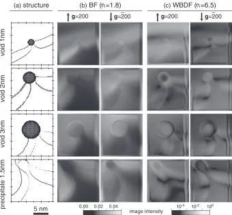
Figures 2(a) and 2(b) compare the cusp structure and typical calculated images at n=1.8. The extra contrast observed at the cell boundaries is the artifact to be ignored. The cusp images for 1 nm void are less clear because of small size and low contrast. The other cusps formed by the strong obstacles are identified by their dark images. The two partial dislocations are not distinguished from each other, which is consistent to a general image of dissociated dislocations in fcc metals under two-beam conditions.12,13)The cusp images depend on the sign of the diffracting vector; the image appears inside and outside the leading partials for g=200 and g¼200, respectively. This contrast variation was common for all the obstacles examined, and would be similar to the“insideoutside”contrast known for dislocation loops of interstitial- and vacancy-types.
Defect images depend also on the specimen geometry. The cusp images showed periodic variations with the specimen thickness t and the depthd of the defect cell; the period of the oscillation was the effective extinction distance ð²effg Þ. Accordingly, Fig. 3, the images with varioustandd for one effective extinction distance, represents all variations.
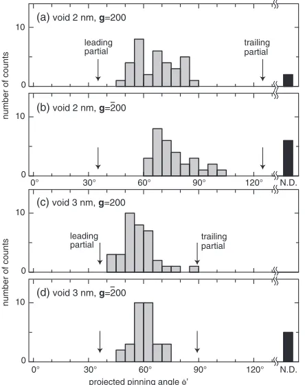
The pinning angle º was defined as the apex angle between the two tangent lines of the dislocation at the obstacle surface. We measured the apex angle onzTEMplane, which is referred to as the projected pinning angle º0, by using either dark or bright image which had larger contrast in each condition in Fig. 3. The angle was not determined when
neither of the images was clear. Several examples of the tangent lines are shown with broken lines in Fig. 3. Figure 4 compares the angle º0 measured on TEM images with the true angles obtained from the configuration of the leading and trailing partials shown in Fig. 2(a). The distribution ranges about 30 degrees, and is between the true angles for the two partials. The angles are slightly larger in the outside contrast condition ðg¼200Þ. The pinning angle of the hard precipitate was zero, which was identified on TEM images both in the inside and outside conditions.
3.2 Weak-beam dark-field images
In the MD simulation the leading and trailing partials have different interaction with an obstacle and have different critical angles.5) The weak-beam dark-field (WBDF) tech-nique might reveal thefine scale behavior of the two partials in a cusp, because dislocation images with narrow width and high contrast lies close to the projection of the dislocation core. We examined the cusp images on weak-beam dark-field images at the deviation parameternbetween 4.5 and 6.5.
Typical weak-beam images of dislocation cusps are shown in Fig. 2(c) using a logarithmic grey scale. Because the scale displays the intensity over a wide range without saturation, detailed contrast that is darker than the backgound may not be observed on practical weak-beam images. The confi g-urations of the two partials are observed at g=200. On reversing the diffracting vector ðg¼ 200Þ, the stacking fault image has larger intensity while dislocation images are not clear. The two partials might be detected as borders of the
void 1nm
void 2nm
void 3nm
precipitate
1.5nm
(b) BF (n=1.8) (c) WBDF (n=6.5)
g=200 g=200 g=200 g=200
5 nm (a) structure
0.00 0.02 0.04
image intensity
100
10-2
10-4
[image:3.595.129.469.69.383.2]stacking fault band. It has been known that stacking fault image shows systematic asymmetry, depending on the sign of
g·R; the bright band corresponds to the strong condition in the asymmetry.12)These image variations were common for the obstacles excepting for 1 nm void. We note that irregular dark bands appear around the obstacle in weak-beam images. Because the position of the band depended on the diffraction condition and the specimen geometry (i.e., the specimen thicknesstand the defect depthd), the band will not represent a certain defect structure but will be similar to a bend contour, suggesting a high strain around the obstacle.
3.3 Discussion
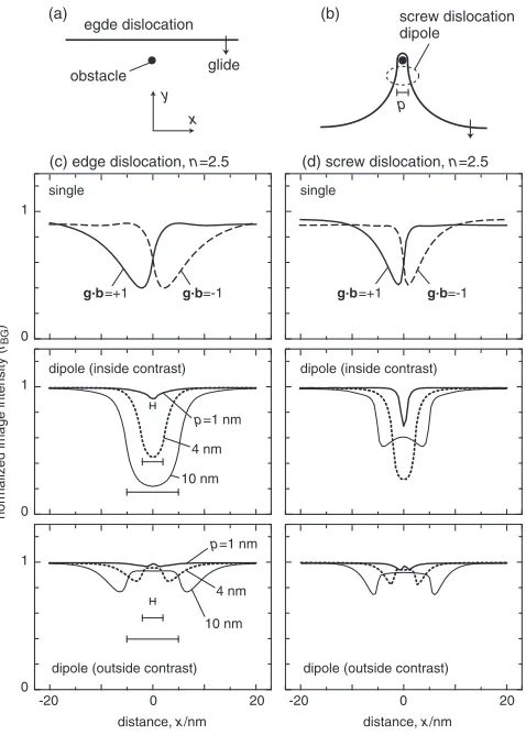
Characteristics of the calculated cusp images could be interpreted from images of a dislocation dipole, i.e., a pair of single straight dislocations of opposite Burgers vectors. Figures 5(a) and 5(b) schematically show that an edge dislocation forms a screw dipole near the obstacle; and
vice versa. The approximation will be better for stronger
obstacle, because the cusp is elongated to form a dipole as the case of the hard precipitate shown in Fig. 2(a). Dipole images are known to show the insideoutside contrast.12,13)Because the two dislocations have opposite Burgers vectors, one image will lie on one side of the core and the other on the opposite side. The order reverses on reversing diffracting vector.
Figures 5(c) and 5(d) compare image intensity profiles among single and dipole perfect dislocations of edge and screw types, lying parallel to the specimen surface. The calculation was based on the multibeam dynamical equations with the column approximation.12) We assumed a strain field of a perfect dislocation in an isotropic medium for the single dislocation and their simple superposition for the dipole. The image intensity was shown as normalized by the background intensity,IBG. The dipole with a small separation, corresponding to a small cusp, has very weak contrast both in inside and outside conditions. This is because the two strain fields with opposite Burgers vectors almost cancel to each other. With increasing separation, the contrast increases for the inside condition because of an additive effect of the two strain fields, while the outside contrast is weaker than that of single dislocations due to a partial cancellation. The characteristics of dislocation cusp images observed in the multislice simulation were interpreted qualitatively by the conventional dynamical theory applied for dislocation dipole. A quantitative difference in the dipole images between edge and screw types would reflect the narrower image for a single screw dislocation.
Finally, we note very briefly another method useful to determine the apex angle:3)the total configuration of bow out dislocation was extrapolated to the cusp with assuming the dislocation configuration that minimized the total elastic energy in the standard line tension model. Understanding
depth of defect cell, d (b)
specimen thickness,
t
(b)
366
390
414
(a) g=200
5 nm
(b) g=200
0.00 0.02 0.04 0.06 image intensity
222 246 270
438
294 222 246 270 294
Fig. 3 Variation of the cusp images for 2 nm void with the sign of the diffracting vector, the specimen thickness, and the depth of the defect cell, atn=1.8ð²effg 96bÞ.
0 10
0 10
0 10
0 10
projected pinning angle φ’
(a) void 2 nm, g=200
120° 90°
60° 30°
0°
(c) void 3 nm, g=200
number of counts
number of counts
leading partial
trailing partial
leading
partial trailingpartial
(b) void 2 nm, g=200
(d) void 3 nm, g=200
N.D. 120° 90°
60° 30°
0° N.D.
[image:4.595.60.282.313.593.2]of characteristics and contrast mechanisms of cusp images presented here as well as the application of the line tension model to the dislocation configuration are expected to reduce errors in measuring the pinning angle on TEM images.
4. Conclusion
We simulated TEM image of the cusp on an edge dislocation that was pinned by an obstacle in copper. In
two-beam brightfield images, large cusps formed by strong obstacles were identified by dark images. The images showed the insideoutside contrast on reversing the diffracting vector and other variations depending on the specimen geometry. Local configurations of dislocation cusps were not always revealed in two-beam conditions. Then the distribution of pinning angles measured on TEM images ranged up to a few tens of degrees and were between the true angles for the two partial dislocations. In some weak-beam dark-field images, the two partial dislocations and the stacking fault were distinguished from one another. Characteristics and contrast mechanisms of cusp images could be interpreted from those of dislocation dipoles. The knowledge of the cusp images is expected to reduce errors in estimating obstacle strength factor using in situstraining experiments.
Acknowledgments
A part of the numerical simulation was performed using the Center for Computational Materials Science, Institute for Materials Research, Tohoku University.
REFERENCES
1) K. Nogiwa, T. Yamamoto, K. Fukumoto, H. Matsui, Y. Nagai, K. Yubuta and M. Hasegawa:J. Nucl. Mater.307311(2002) 946. 2) K. Nogiwa, N. Nita and H. Matsui:J. Nucl. Mater.367370(2007)
392.
3) K. Nogiwa: Doctorate thesis, (Tohoku University, 2007).
4) S. Y. Hu, S. Schmauder and L. Q. Chen:Phys. Stat. Sol. B220(2000) 845.
5) Yu. N. Osetsky, D. J. Bacon and V. Mohles:Philos. Mag.83(2003) 3623.
6) T. Hatano and H. Matsui:Phys. Rev. B72(2005) 094105. 7) T. Hatano:Phys. Rev. B74(2006) 020102(R).
8) G. J. Ackland, D. J. Bacon, A. F. Calder and T. Harry:Philos. Mag. A 75(1997) 713.
9) G. Radi:Acta Crystallogr. A26(1970) 41.
10) Y. Satoh, H. Taoka, S. Kojima, T. Yoshiie and M. Kiritani:Philos. Mag. A70(1994) 869.
11) Y. Satoh, T. Yoshiie, Y. Matsukawa and M. Kiritani:Mater. Sci. Eng. A 350(2003) 207215.
12) P. B. Hirsch, A. Howie, R. B. Nicholson, D. W. Pashley and M. J. Whelan:Electron Microscopy of Thin Crystals, 2nd edition, (Kreiger Publishing Co., 1977).
13) D. B. Williams and C. B. Carter:Transmission Electron Microscopy, (Prenum Press, 1996).
(c) edge dislocation, n=2.5 (d) screw dislocation, n=2.5
single
dipole (inside contrast)
dipole (outside contrast)
0 20
-20 -20 0 20
distance, x/nm
normalized image intensity (
IBG
)
0 1 0 1 0 1
single
dipole (inside contrast)
dipole (outside contrast) 10 nm
4 nm
p=1 nm
g.b=+1 g.b=-1 g.b=+1 g.b=-1
(a)
glide obstacle
screw dislocation dipole
(b)
p
10 nm 4 nm
p=1 nm egde dislocation
distance, x/nm
x y
[image:5.595.52.291.69.403.2]