http://go.warwick.ac.uk/lib-publications
Original citation:
New, Edward, Howells, Thomas, Sullivan, Paul J. and Jones, Tim S.. (2013) Small
molecule tandem organic photovoltaic cells incorporating an α-NPD optical spacer layer.
Organic Electronics, Volume 14 (Number 9). pp. 2353-2359. ISSN 1566-1199
Permanent WRAP url:
http://wrap.warwick.ac.uk/55448
Copyright and reuse:
The Warwick Research Archive Portal (WRAP) makes this work of researchers of the
University of Warwick available open access under the following conditions.
This article is made available under the Creative Commons Attribution 3.0 Unported (CC
BY 3.0) license and may be reused according to the conditions of the license. For more
details see:
http://creativecommons.org/licenses/by/3.0/
A note on versions:
The version presented in WRAP is the published version, or, version of record, and may
be cited as it appears here.
Small molecule tandem organic photovoltaic cells incorporating
an
a
-NPD optical spacer layer
q
Edward New, Thomas Howells, Paul Sullivan
⇑, Tim S. Jones
⇑Department of Chemistry, University of Warwick, Coventry CV4 7AL, UK
a r t i c l e
i n f o
Article history:
Received 16 January 2013
Received in revised form 24 May 2013 Accepted 26 May 2013
Available online 7 June 2013
Keywords:
Tandem organic photovoltaics Boron subphthalocyanine Molybdenum oxide Optical spacer
a-NPD
a b s t r a c t
We report an improvement in power conversion efficiency in a small molecule tandem organic photovoltaic (OPV) device by the optimisation of current balancing of the sub-cells using an optical spacer layer. A co-deposited layer ofN,N’-bis(1-naphthyl)-N,N0
-diphenyl-1,1’-biphenyl-4,4’-diamine (a-NPD) and molybdenum oxide was used as the optical spacer layer and provided a highly transparent and conductive layer. Optical simulations showed the addition of the optical spacer in a boron subphthalocyanine (SubPc)/C60based tandem
OPV device increased the SubPc absorption in the front sub-cell and resulted in current bal-ancing through the device. Fabricated tandem OPV devices showed similar trends, with the power conversion efficiency increasing from 2.3% to 4.2% with the addition of an optimised optical spacer thickness. External quantum efficiency and total absorption efficiency mea-surements back up the optical model data which attribute the increased performance to improved SubPc absorption in the front sub-cell, balancing the photocurrents of the two sub-cells.
Ó2013 The Authors. Published by Elsevier B.V. All rights reserved.
1. Introduction
Organic photovoltaic cells (OPVs) have attracted much attention recently due to their promise for low cost power generation [1]. Power conversion efficiencies (PCE) have increased steadily over the past few years but are still lim-ited by light absorption of the thin active layers and low coverage of the solar spectrum [2]. Methods have been introduced to overcome these problems, including bulk heterojunction (BHJ) layers to improve exciton dissociation
[3,4], allowing for thicker active layers to be used for en-hanced light absorption. To increase the cell efficiency fur-ther, tandem cell architectures have been introduced
comprised of sub-cells with complementary absorption spectra to improve the overall absorption[5–9]. Tandem cells comprised of identical composition sub-cells have also been used though performance enhancement is lower due to the absorption overlap[10,11]. As a result of the use of a reflective cathode and the formation of optical inter-ference patterns in the structure, the design of the tandem stack to optimise the position of the sub-cells relative to the reflecting cathode becomes important to match the photocurrents of the two sub-cells[12,13]. This can usually be achieved by the use of an optical spacer layer, such as poly(trifluoroethylene) (PTrFE)[14], TiOX[8]or ZnO[15]. Wide band gap organic semiconductors are suitably trans-parent for use as a spacer layer, but usually have low con-ductivity, although this has been overcome by electrically
doping the layers [16]. Small molecule tandem cells
employing a highly doped optical spacer layer have achieved very high performances but these usually require the use of expensive dopant materials, such as F4-TCNQ, increasing the cost of production [17]. N,N’ -bis(1-naph-thyl)-N,N’-diphenyl-1,1’-biphenyl-4,4’-diamine (
a
-NPD)1566-1199/$ - see front matterÓ2013 The Authors. Published by Elsevier B.V. All rights reserved.
http://dx.doi.org/10.1016/j.orgel.2013.05.037 q
This is an open-access article distributed under the terms of the Creative Commons Attribution License, which permits unrestricted use, distribution, and reproduction in any medium, provided the original author and source are credited.
⇑Corresponding authors. Tel.: +44 (0)2476 522188 (P. Sullivan), +44 (0)2476 528265 (T. S Jones).
E-mail addresses:[email protected](P. Sullivan), [email protected](T.S. Jones).
Contents lists available atSciVerse ScienceDirect
Organic Electronics
has been used effectively as a wide band gap hole trans-porting layer in organic light emitting diodes[18]and fur-ther improvements in conductivity have been shown by doping the layer with a small amount of molybdenum oxide (MoOX)[19]. In this study, we show that co-deposi-tion of
a
-NPD with a low weight% of MoOXproduces an effective hole transporting optical spacer layer that, upon optimisation, leads to efficient small molecule tandem OPV cells. This shows that efficient tandem OPV devices can be achieved using an optical spacer without the use of an expensive, highly volatile, dopant.2. Experimental
All devices were produced on indium tin oxide (ITO) coated glass substrates (Thin Film Devices Inc.) with a sheet resistance of 15Xsq1. The substrates were cleaned
using organic solvents in an ultrasonic bath and exposed to UV–ozone prior to use. The organic materials, C60(Nano-C
Inc, 99.5%) and
a
-NPD (Aldrich, 96%) were purified by vac-uum gradient sublimation prior to deposition, whilst boron subphthalocyanine chloride (SubPc, Lumtec, 99%), MoOX (Aldrich, 99.99%) and bathocuproine (BCP, Aldrich 98%) were used as received. The layers were vacuum deposited using a Kurt J. Lesker Spectros system. For the BHJ Sub-Pc:C60 anda
-NPD:MoOX layers, the mass ratio was con-trolled by independent quartz crystal microbalance measurements. The Al cathode was deposited in situ through a shadow mask giving devices with an active area of 0.16 cm2. The current–voltage (J–V) characteristics ofthe cells were measured under simulated AM1.5G solar illumination at 100 mW cm2from a Newport Oriel solar
simulator using a Keithley 2400 sourcemeter for current detection. External quantum efficiency (EQE) and total absorption efficiency (TAE) measurements were performed using mechanically chopped monochromatic light from a Xe arc lamp (Sciencetech SF150). Signal detection was per-formed using a current–voltage preamplifier (Femto DHPCA-100) and a lock-in amplifier (Stanford Research SR 830 DSP). Optical electric field calculations were carried
out using the transfer matrix formalism [20,21] with
refractive index data of the SubPc:C60films measured by
L.O.T-Oriel GmbH & Co. KG with data for all other layers ta-ken from the literature[22,23]. Work function measure-ments were carried under nitrogen using a Kelvin Probe (Besocke Delta Phi GmbH) and referenced to freshly cleaved highly oriented pyrolytic graphite.
3. Results and discussion
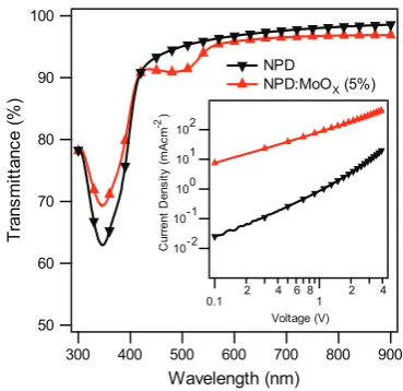
Fig. 1shows the transmittance spectra of an
a
-NPD filmand a codeposited film of
a
-NPD:MoOX (5%). The large3.05 eV band gap of
a
-NPD gives the film a high transpar-ency in the visible region of over 90% above 400 nm, and the main absorption from the film is in the UV region. The co-deposited filma
-NPD:MoOX(5%) shows a slight in-crease in transmittance at 350 nm and a dein-crease at 450– 500 nm caused by the reduction in intrinsica
-NPD and radical cations in thea
-NPD generated by charge transfer to the MoOX[24]. The conductivity of the two films wasinvestigated by analysis of theJ–Vcharacteristics of hole only devices. These were fabricated with the structure ITO/MoOX (10 nm)/
a
-NPD (0, 5% MoOX) (100 nm)/MoOX (10 nm)/Al, with the hole transport layer (HTL) sand-wiched between two MoOXlayers acting as ohmic contacts to the electrodes. The results are also shown inFig. 1, and a large increase in conductivity is seen for thea
-NPD:MoOX layer which passes an order of magnitude higher current with forward bias than thea
-NPD film. This is explained by charge transfer of an electron from the highest occupied molecular orbital (HOMO) ofa
-NPD to the valence band ofthe MoOX leaving behind a vacant hole which can help
facilitate hole transport [19]. The origin of this charge transfer has been determined from the dispersion effi-ciency of small nanoclusters of MoOX within the
a
-NPD film[25].The electrical doping present in the
a
-NPD:MoOXfilm not only improves the conductivity, but also leads to a shift in the Fermi level towards the HOMO ofa
-NPD, reducing the interface barrier for hole injection. Work function mea-surements were carried out ona
-NPD films in a nitrogen atmosphere and the results are shown in Fig. 2. In the intrinsic film the Fermi level sits 1.1 eV above the HOMO and on addition of a small percentage of MoOX(5%) a rapid shift of over 0.5 eV is seen towards the HOMO. With fur-ther increases in MoOXconcentration there is little change in the Fermi level position which is pinned at 0.5 eV above the HOMO consistent with previous reports [19]. The properties of thea
-NPD:MoOX film, namely its high transmittance in the visible region, the shift of the Fermi level towards the HOMO ofa
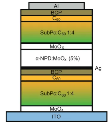
-NPD reducing the injection barrier for holes, and the increase in conductivity, are all desirable for application as an optical spacer layer.Fig. 3shows a schematic of the tandem device structure investigated to assess the influence of the
a
-NPD:MoOX optical spacer layer. The active layers are based upon boron subphthalocyanine chloride (SubPc) and C60bulk [image:3.544.303.488.51.230.2]hetero-juntions with a 1:4 weight ratio[26]. The
a
-NPD opticalFig. 1.Transmittance spectra ofa-NPD anda-NPD:MoOX(5%) layers on
quartz glass. Inset:J–Vcharacteristics of hole only devices; ITO/MoOX
(5 nm)/HTL (100 nm)/MoOX (5 nm)/Al with a HTL of a-NPD and a
-NPD:MoOX(5%) respectively.
spacer layer is placed between the Ag recombination layer and the MoOX hole transport layer, allowing for optical spacing of the front SubPc:C60sub-cell whilst acting as a
hole transport layer for the back sub-cell to the recombina-tion layer. The performance of single BHJ devices using an
a
-NPD:MoOXhole transport layer was found to be largelyindependent of MoOX concentration in the range 5–25%
(SupplementaryFig. S1andTable T1), and therefore a 5% concentration was selected for the optical spacer layers.
The tandem device had the structure ITO/MoOX (5 nm)/
SubPc:C60 (1:4) (70 nm)/C60 (10 nm)/BCP (5 nm)/Ag
(0.3 nm)/
a
-NPD:MoOX(5%) (0–80 nm)/MoOX (5 nm)/Sub-Pc:C60 (1:4) (65 nm)/C60 (10 nm)/BCP (8 nm)/Al. Thea
-NPD:MoOX thickness was varied to investigate the influ-ence on device performance of spacing the front sub-cell away from the Al cathode. The varying distance of the sub-cell from the Al cathode alters its position in the opti-cal field and varies the sub-cell photocurrent, thus provid-ing an effective tool for balancprovid-ing the photocurrents of both sub-cells.
In order to investigate the current balancing of the sub-cells an optical model was used to calculate the photocur-rent produced in each of the sub-cells with a varied
a
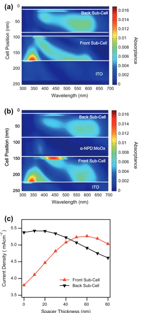
-NPD:MoOXspacer thickness. The transfer matrix formalism[20]was used to calculate the absorptance throughout the device using the optical data of the films.Fig. 4shows the wavelength dependent absorptance in the layers for the device without an optical spacer (4a) and with a 50 nm
a
-NPD:MoOX layer (4b). The device without an optical spacer has a large absorptance in the back sub-cell be-tween 500 and 600 nm from the contribution of SubPc and 400–500 nm from C60. In the front sub-cell there isconsiderably less absorptance in the SubPc region. With the spacer layer, absorptance is still strong in the SubPc section in the back sub-cell but an enhancement is seen in this region in the front sub-cell. The optical spacer has positioned the sub-cell into an interference peak for radia-tion of 500–600 nm. The absorptance of C60 in the 400–
500 nm section also varies with the spacer layer, with the absorptance peaking in the discrete C60layer in the front
sub-cell and a small reduction seen in the BHJ layer. The absorptance profiles of the devices were integrated over the AM1.5G solar spectrum to calculate the predicted sub-cell photocurrents. An internal quantum efficiency of 0.8 was assumed, calculated from comparison of the absorptance of an equivalent single junction device to the measured external quantum efficiency (EQE) (supplemen-taryFig. S2). A plot of the predicted photocurrent of both sub-cells with spacer thickness is shown inFig. 4c. A large photocurrent imbalance is shown for a spacer thickness of 0 nm from the low SubPc contribution in the front sub-cell. The photocurrent from this sub-cell improves with in-creased optical spacer thickness as it is moved into an opti-mum optical interference position with a spacer thickness of 60 nm. This increased absorptance in the front sub-cell has a negative effect on the back sub-cell, reducing its pho-tocurrent with increased spacer thickness. An optimum current balancing is observed for an optical spacer thick-ness just above 40 nm with a predicted photocurrent of 5.1 mA cm2, a 35% increase in the minimum sub-cell
pho-tocurrent from the device without an optical spacer layer.
α -NPD 5.5 eV
α -NPD: MoOX(20%)
(b)
1.1
1.0
0.9
0.8
0.7
0.6
0.5
0.4
EF
- H
O
M
O
(eV
)
30 25 20 15 10 5 0
MoOX weight %
(a)
EF
HOMO LUMO VL
φ = 4.4 eV
[image:4.544.70.223.55.369.2]φ = 4.9 eV
Fig. 2. (a) Energy difference between the Fermi level and the HOMO level of ana-NPD:MoOXfilm with different MoOXconcentrations. The work
function was measured using Kelvin Probe and the HOMO level taken from the literature.[19] The dotted line is a guide for the eye. (b) Schematic energy level diagrams showing the Fermi level shift towards thea-NPD HOMO.
SubPc:C
601:4
C
60BCP
SubPc:C
601:4
MoO
xBCP
α-NPD:MoOx
(5%)
C
60MoOx
ITO
Al
Ag
Fig. 3.Schematic of the SubPc:C60tandem OPV device investigated with
[image:4.544.52.236.449.656.2]A similar spacing effect could also be achieved through increasing the active layer thicknesses, and indeed model-ling predicts higher limiting photocurrents for an ideal de-vice (supplementaryFig. S3). However, significant FF losses have been reported at small molecule BHJ thicknesses over 80 nm, significantly below the required thicknesses of >100 nm here, and therefore any photocurrent gain is likely to be negated by a loss in FF[27].
A series of devices were fabricated with nine variations of
a
-NPD:MoOXthickness from 0–80 nm. Due to the vac-uum deposition method, nine different thicknesses ofa
-NPD:MoOXcould be processed during the same fabrication run with all other layers remaining identical across all de-vices, allowing direct measurement of the optical spacer effect without batch to batch variations of the photoactive layers. The device parameters for the fabricated cells areWavelength (nm)
Cell Position (nm)
300 350 400 450 500 550 600 650 700 0
50
100
150
200
250 0
0.002 0.004 0.006 0.008 0.01 0.012 0.014 0.016
Wavelength (nm)
Cell Position (nm)
300 350 400 450 500 550 600 650 700 0
50
100
150
200
250 0
0.002 0.004 0.006 0.008 0.01 0.012 0.014 0.016
(a)
Front Sub-Cell Back Sub-Cell
ITO
α-NPD:MoOx
5.5
5.0
4.5
4.0
3.5
80 60
40 20
0
Front Sub-Cell Back Sub-Cell
(b)
(c)
Front Sub-Cell Back Sub-Cell
ITO
Absorptance
Absorptance
Cell Position (nm)
0
50
100
150
200
250
Front Sub-Cell Back Sub-Cell
ITO
α-NPD:MoOx
Current Density ( mAcm
-2 )
Spacer Thickness (nm)
Front Sub-Cell Back Sub-Cell
[image:5.544.159.400.50.569.2]ITO
Fig. 4.Wavelength dependant absorptance through the layers calculated in the SubPc:C60tandem OPV device with (a) no optical spacer layer and (b) a
shown inFig. 5. As expected from the modelled data, the change in absorptance of the sub-cells with varying spacer thickness causes a large variation in JSC. An improvement in
photocurrent is shown on the addition of an optical spacer, with the JSCimproving from 3.2 mA cm2without a spacer
layer, to 4.7 mA cm2 with an optimum 60 nm spacer
thickness. This improvement in JSC is indicative of the absorptance increase in the front sub-cell as it moves into a maxima in the optical field (Fig. 4), leading to improved
current balancing of the sub-cells. The VOC shows an
improvement on addition of the spacer from 1.72 V to 2.07 V and it remains constant with increased thickness of the spacer layer, close to the summation of the two sin-gle cell voltages (1.07 V). This shows the effectiveness of utilising the
a
-NPD:MoOXlayer in the recombination zone, leading to a lower voltage loss. The FF remains consistent across alla
-NPD:MoOX thicknesses indicating low resis-tance losses from the spacer layer due to its high conduc-tivity[12]. Due to the consistentVOCand FF with spacer thickness, the trend in PCE follows the JSC. The low JSCandVOCof the reference device produce a PCE of 2.3%. De-vice performance improves rapidly with the addition of an optical spacer layer and PCE reaches 4.2%, an increase of 80% from optimisation of the absorptance in both sub-cells. Comparing the tandem device to a representative sub-cell with BHJ thickness of 65 nm, an improvement in performance is also seen. TheJSCof the tandem device is
slightly reduced from the single-junction device value of 6.6 mA cm2due to the absorption now being spread
be-tween two sub-cells, but the efficiency is improved from
3.3%. TheJ–Vplots for this device and performance param-eters are shown in SupplementaryFig. S4.
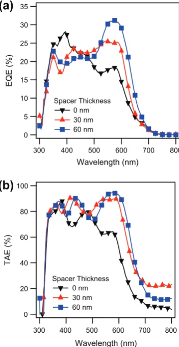
To further investigate the cause of the increase in pho-tocurrent when an optical spacer is added in-between the sub-cells, EQE measurements were performed. These were carried out in monochromatic light conditions with no external light or voltage bias. Under these measurement conditions any imbalance in the current generation of the two sub-cells will result in the EQE being limited as the underperforming sub-cell prevents the overperforming sub-cell from operating at its full capacity.Fig. 6a shows the EQE measurements of the devices with a 0, 30 and 60 nm thick
a
-NPD:MoOXoptical spacer. The reference de-vice without the spacer layer showed an EQE of 17% at the SubPc absorption peak (590 nm). The device with the 30 nm optical spacer shows an improvement from 500 to 600 nm with a peak of 24% from an increased contribution of the SubPc. This further improves with the 60 nm optical spacer where the peak at 590 nm is >30%. This increase in the SubPc EQE shows the improvements in the sub-cell balancing in this absorption region as seen in the optical model (Fig. 4b), with an increase in SubPc absorptance from 500 to 600 nm in the front sub-cell on the addition(a)
(b)
4.5 4.0 3.5 3.0 2.5 JSC mAcm -2 PCE (%) 80 60 40 20 0Spacer Thickness (nm)
2.4 2.2 2.0 1.8 1.6 1.4 1.2 1.0 VOC (V) 80 60 40 20 0
Spacer Thickness (nm)
[image:6.544.304.480.323.663.2]0.55 0.50 0.45 0.40 0.35 FF
Fig. 5. Performance characteristics of the SubPc: C60BHJ tandem OPV
device versus spacer layer thickess; (a)JSCand PCE (b)VOCand FF.
100 80 60 40 20 0 TAE (%) 800 700 600 500 400 300 Wavelength (nm) Spacer Thickness 0 nm 30 nm 60 nm 35 30 25 20 15 10 5 0 EQE (%) 800 700 600 500 400 300 Wavelength (nm) Spacer Thickness 0 nm 30 nm 60 nm
(a)
(b)
Fig. 6.(a) EQE spectra and (b) TAE spectra of the SubPc:C60BHJ tandem
[image:6.544.61.237.387.664.2]of an optical spacer. The shift in absorptance profile of the C60region seen inFig. 4provides no significant
improve-ment in the EQE between 400 and 450 nm.
TAE measurements were also carried out on the devices and are shown inFig. 6b. These are recorded from reflec-tion data, and provide a measure of all light absorbed in the device. The device without the optical spacer has a low absorption at the SubPc peak (590 nm). An increase in absorption is seen with addition of the
a
-NPD:MoOX optical spacer which occurs in the 500–600 nm region cor-responding to the SubPc, similar to the improvement seen in the EQE. The TAE of the devices with 30 and 60 nm spacer layers show only a small change in the SubPc absorption region compared to the variation seen in the EQE. This suggests that the distribution of the absorption within the sub-cells produces an improved current match-ing in the 60 nm optical spacer device whilst havmatch-ing a sim-ilar overall absorption to the 30 nm optical spacer device. The TAE measurements corroborate the EQE and the opti-cal modelling data suggesting that the increase inJSCof the tandem device is from increased absorption of the SubPc in the front tandem sub-cell, balancing the photocurrents through the device.4. Conclusions
In this paper we have demonstrated the use of an
a
-NPD:MoOX layer as a conductive and visibly transparent optical spacer layer for small molecule tandem OPV de-vices. Optical simulations showed that photocurrent in the tandem device could be enhanced by placing the sub-cells in interference maxima by inserting an optical spacer layer of 40–60 nm. Photocurrent in the tandem OPV device improved from 3.2 mA cm2to 4.7 mA cm2due to theen-hanced absorption resulting in current balancing between sub-cells. External quantum efficiency and total absorption efficiency measurements showed that the increase in absorption in the SubPc region was the cause for the im-proved photocurrent balancing of the sub-cells in the opti-cally spaced tandem OPV device improving the efficiency
by80%.
Acknowledgements
This work was supported by the Engineering and Phys-ical Sciences Research Council [Grant Number EP/ G031088/1]. The University of Warwick is thanked for the award of a postgraduate scholarship for Edward New. Dr. Ross A. Hatton is thanked for use of the Kelvin Probe. Prof. Jenny Nelson and Dr. Felix Braun are thanked for pro-vision of the transfer matrix script for optical modelling.
Appendix A. Supplementary material
Supplementary data associated with this article can be found, in the online version, athttp://dx.doi.org/10.1016/ j.orgel.2013.05.037.
References
[1]M. Riede, T. Mueller, W. Tress, R. Schueppel, K. Leo, Small-molecule solar cells – status and perspectives, Nanotechnology 19 (2008) 424001.
[2]A. Mishra, P. Bauerle, Small molecule organic semiconductors on the move: Promises for future solar energy technology, Angew. Chem.-Int. Ed. 51 (2012) 2020–2067.
[3]P. Peumans, S. Uchida, S.R. Forrest, Efficient bulk heterojunction photovoltaic cells using small-molecular-weight organic thin films, Nature 425 (2003) 158–162.
[4]P. Sullivan, S. Heutz, S.M. Schultes, T.S. Jones, Influence of codeposition on the performance of CuPc-C-60 heterojunction photovoltaic devices, Appl. Phys. Lett. 84 (2004) 1210–1212. [5]A. Hadipour, B. de Boer, J. Wildeman, F.B. Kooistra, J.C. Hummelen,
M.G.R. Turbiez, M.M. Wienk, R.A.J. Janssen, P.W.M. Blom, Solution-processed organic tandem solar cells, Adv. Funct. Mater. 16 (2006) 1897–1903.
[6]D. Cheyns, B.P. Rand, P. Heremans, Organic tandem solar cells with complementary absorbing layers and a high open-circuit voltage, Appl. Phys. Lett. 97 (2010) 033301.
[7]T. Ameri, G. Dennler, C. Lungenschmied, C.J. Brabec, Organic tandem solar cells: A review, Energy Environ. Sci. 2 (2009) 347–363. [8]J.Y. Kim, K. Lee, N.E. Coates, D. Moses, T.Q. Nguyen, M. Dante, A.J.
Heeger, Efficient tandem polymer solar cells fabricated by all-solution processing, Science 317 (2007) 222–225.
[9]T. Howells, E. New, P. Sullivan, T.S. Jones, An external quantum efficiency technique to directly observe current balancing in tandem organic photovoltaics, Adv. Energy Mater. 1 (2011) 1085–1088. [10] V. Steinmann, N.M. Kronenberg, M.R. Lenze, S.M. Graf, D. Hertel, K.
Meerholz, H. Bürckstümmer, E.V. Tulyakova, F. Würthner, Simple highly efficient vacuum-processed bulk heterojunction solar cells based on merocyanine dyes, Adv. Energy Mater. 1 (2011) 888– 893.
[11]M. Zhang, H. Wang, C.W. Tang, Tandem photovoltaic cells based on low-concentration donor doped C60, Org. Electron. 13 (2012) 249– 251.
[12]R. Schueppel, R. Timmreck, N. Allinger, T. Mueller, M. Furno, C. Uhrich, K. Leo, M. Riede, Controlled current matching in small molecule organic tandem solar cells using doped spacer layers, J. Appl. Phys. 107 (2010) 044503.
[13]P. Sullivan, S. Schumann, R. Da Campo, T. Howells, A. Duraud, M. Shipman, R.A. Hatton, T.S. Jones, Ultra-High Voltage Multijunction Organic Solar Cells for Low-Power Electronic Applications, Adv. Energy Mater. 3 (2013) 239–244.
[14]A. Hadipour, B. de Boer, P.W.M. Blom, Solution-processed organic tandem solar cells with embedded optical spacers, J. Appl. Phys. 102 (2007) 074506.
[15]J. Gilot, I. Barbu, M.M. Wienk, R.A.J. Janssen, The use of ZnO as optical spacer in polymer solar cells: Theoretical and experimental study, Appl. Phys. Lett. 91 (2007) 113520.
[16]B. Maennig, J. Drechsel, D. Gebeyehu, P. Simon, F. Kozlowski, A. Werner, F. Li, S. Grundmann, S. Sonntag, M. Koch, K. Leo, M. Pfeiffer, H. Hoppe, D. Meissner, N.S. Sariciftci, I. Riedel, V. Dyakonov, J. Parisi, Organic p-i-n solar cells, Appl. Phys. a-Mater. 79 (2004) 1–14. [17]M. Riede, C. Uhrich, J. Widmer, R. Timmreck, D. Wynands, G.
Schwartz, W.M. Gnehr, D. Hildebrandt, A. Weiss, J. Hwang, S. Sundarraj, P. Erk, M. Pfeiffer, K. Leo, Efficient organic tandem solar cells based on small molecules, Adv. Funct. Mater. 21 (2011) 3019– 3028.
[18]M. Baldo, S. Lamansky, P. Burrows, M. Thompson, S. Forrest, Very high-efficiency green organic light-emitting devices based on electrophosphorescence, Appl. Phys. Lett. 75 (1999) 4–6. [19]M. Kroger, S. Hamwi, J. Meyer, T. Riedl, W. Kowalsky, A. Kahn, P-type
doping of organic wide band gap materials by transition metal oxides: A case-study on Molybdenum trioxide, Org. Electron. 10 (2009) 932–938.
[20] L.A.A. Pettersson, L.S. Roman, O. Inganas, Modeling photocurrent action spectra of photovoltaic devices based on organic thin films, J. Appl. Phys. 86 (1999) 487–496.
[21]G.F. Burkhard, E.T. Hoke, M.D. McGehee, Accounting for interference scattering, and electrode absorption to make accurate internal quantum efficiency measurements in organic and other thin solar cells, Adv. Mater. 22 (2010) 3293–3297.
[22]D. Datta, S. Kumar, Growth and ellipsometric studies on C-60 thin films for solar cell applications, J. Appl. Phys. 106 (2009) 074517. [23]C. Himcinschi, N. Meyer, S. Hartmann, M. Gersdorff, M. Friedrich, H.
Johannes, W. Kowalsky, M. Schwambera, G. Strauch, M. Heuken, D. Zahn, Spectroscopic ellipsometric characterization of organic films
obtained via organic vapor phase deposition, Appl. Phys.a-Mater.Sci. Process. 80 (2005) 551–555.
[24]T. Matsushima, Y. Kinoshita, H. Murata, Formation of ohmic hole injection by inserting an ultrathin layer of molybdenum trioxide between indium tin oxide and organic hole-transporting layers, Appl. Phys. Lett. 91 (2007) 253504.
[25]J. Lee, H. Kim, K. Kim, J. Kim, Origin of charge generation efficiency of metal oxide p-dopants in organic semiconductors, Org. Electron. 12 (2011) 950–954.
[26]R. Pandey, R. Holmes, Graded donor–acceptor heterojunctions for efficient organic photovoltaic cells, Adv. Mater. 22 (2010) 5301– 5305.