Hardware Reference Manual
Octal Serial Interface
O~tal
Serial Interface
Central Data Corporation
1602 Newton Drive
Champaign, IL
61820
Phone:
(217) 359-8010
1.
2.
3.
4.
5.
6.
TABLE OF CONTENTS
General Information.
. . .
.
. .
. . .
.
. . .
. .
. . .
Functional Description ••
Principles of Operation ••
Addressing •••••
Bus Interface.
USART Section.
Installation/User Selectable Options ••
Addressing ••••••••.••••
CTS Selection •.••
~•.•••••
Interrupt Selections ••••••
XACK and AACK Generation.
Specifications.
Schematics •••••
1
2
3
3
4
5
7
7
7
7
8
10
13
1.
General Information
The Central Data Octal Ser ial Interface board
is
designed to
expand the serial I/O capacity of any Multibus
system.
The
board
uses
the Signetics 2651 USART
(Universal Synchronous/
Asynchronous Receiver/Transmitter)
as the parallel to serial
converter,
and
allows
independent
baud
rates
(transmission
speeds) to be set for each of the board's eight channels.
The
board supports standard EIA RS-232
interfaces, with the'
following pins used:
TXD, RxD, DSR, CTS, DTR, and RTS.
The
board is capable of operating at baud rates ranging from 50 to
19,200 baud, and can be interrupt driven if so desired.
Also,
the board supports 16-bi t I/O addressing as called for in the
Multibus specification, with an option to use only 8-bit I/O
addresses.
The board drives both the XACK and AACK lines of the Multibus to
allow for the greatest flexibility.
It can return either signal
from
O-BOOns
after
the
receipt
of
a
command,
in
lOOns
increments.
It is suggested that XACK be strapped to be equal to
the access time of the board, while AACK can be strapped to allow
the fastest possible system operation.
2.
Functiona1 Description
The .Octal Serial Interface board is divided into several major
sections, which are described briefly below.
For more detailed
information, refer to the Principles of Operation section of this
manual.
The addressing section of the board consists of the I/O address
comparator
and
the chip-select generation circuitry for
the
USARTs.
The board requires 32 I/O ports, which can be located on
any 32-port boundary.
Dip-switch I/O addressing allows the user
to select the address of the board using either an 8- or l6-bit
I/O address.
With this ability, the board can work equally well
in systems which generate a full l6-bit I/O address as well as in
older 8-bit systems.
The bus interface of the board consists of the data bus buffers,
interrupt circui try, and the XACK/AACK generation logic.
The
data bus is buffered into and out of the board, and interrupts
can be generated on the occurrence of any receiver full or
transmitter empty condition.
Finally, the XACK/AACK generation
circuitry acknowledges all commands to the board and allows the
system to run at the maximum possible speed.
Finally, the USART section is the actual interface to the
exter-nal devices.
This section is repeated on the board eight times,
which gives eight totally independent channels.
The inter face
3.
principles of Operation
This
chapter
details the operation of the entire interface
board.
Any signal names in this text followed by a slash (/)
indicate that the signal is active-low.
As is all Central Data schematics, a grid system is provided to
help locate sources and destinations of signals.
The source of
any named signal will have references to all locations on the
schematics where the signal is used.
At each location where a
signal is used, a reference is given to where it was generated.
If the location is on the same sheet as it is being referenced,
it will show only a grid location (Le. D2).
If, however, the
referenced signal appears on a separate page, it will have the
grid location preceded by the sheet number (i.e. 2-B5).
Addressing
Sheet I of the schematics includes the addressing circuitry for
the board.
The addressing function consists of determining when
the board should be enabled as well as which USART is being
accessed.
The board requires the use of 32 of the system's I/O ports.
These ports can be started on any 32-port boundary, using either
8- or 16-bit addresses.
All of the address lines from the Multibus
74LS04 gates.
The buffered address lines
address
decoding
circuitry
(A5-AI5)
and
circuitry (AO-A4).
are buffered through
are then routed to
to
chip
selection
The address decoding circui t
consists of eleven 74LS266 open
collector exclusive-NOR gates.
All of the outputs of the gates
are tied together, allowing any of the gates to pull the output
low if its inputs do not match.
If all of the pairs of inputs
match, the common output is pulled high by a resistor to +5V.
One input from each of the gates goes to a buffered address line,
wi th the other going to a dip-switch.
This dip-switch, when
closed, causes the corresponding gate input to become grounded.
Under this circumstance, the address line leading to the same
gate must also be low for the board to be addressed.
If the
To allow the selection between 8- and'16-bit I/O addressing, the
outputs of the gates related to A8-A15 are connected through a
shorting plug to the outputs of the gates related to A5-A7.
If
the shorting plug is installed, then the board decodes the full
16-bi t address bus.
If the shorting plug is removed, then the
upper eight gates will not drive the common output, and thus only
the lower three (A5-A7) are used for addressing.
When the address comparator is equal, pin 6 of IC39 will go
high.
This line is used in conjunction with pin 5 to enable the
74LSl38 decoder.
Pin 5
is low whenever
an I/O command
is
currently on the bus.
When the 74LSl38 is enabled, it uses the next lower three address
lines (A4, A3, and A2) to select which USART should be enabled.
In this manner, each USART has four consecutive addresses, for
both reading and writing.
The output of the decoder drives the
chip-select pins of the USARTs.
The R/W/ line of the USART is
used to determine if a read or write operation is to occur when
the chip is selected.
When this line is high, a wr i te will
occur, while in read mode the line will be low.
In summary, the board uses 32 of the I/O ports on the system.
The base address for these ports is selected wi th dip-switches,
and the 32 ports are divided equally among the USARTs.
Bus Interface
The bus inter face consists of the buffer ing circuits required
from the Multibus, the interrupt driver, and the XACK/AACK
gener-ation logic.
The bus interface circuitry is also found on sheet
I of the schematics.
The data bus buffers consist of two 74LS242s, each one buffering
four data lines.
These are inverting buffers, thus immediately
correcting for the inverted data on the bus.
Since, the
direc-tional enable pins of the buffers are of opposite polarity, they
can be tied
together~and are driven by a signal (pin 8 of IC28)
which goes high whenever the board is addressed and an I/O read
command is in progress.
During all other conditions, this signal
is low, thus sending data from the Multibus into the board.
The IORC/ and IOWe/ signals from the Multibus are also buffered
(through 74LS08 gates) and used to set the level of the R/W/ line
on the USARTs.
form an interrupt signal to the processor.
If ei ther the TINT/
or the RINT/ signal goes low, and it is jumpered into pin 8 of
IC29 (with shorting plugs), it will cause a vectored interrupt to
be generated on the selected line.
The board generates two command acknowledge signals.
The first,
XACK,
indicates when
a
data
transfer
is complete
and
the
processor can go to the next cycle.
The other, AACK, gives the
processor advance information related to when a transfer will be
complete.
The circuit which generates the acknowledge signals consists of a
shift register (74LS164, IC25) which is kept cleared when the
board is not active.
When an I/O command occurs, the clear input
goes high, allowing the register to shift lIs through at the CCLK
rate.
The eight outputs of the shift register, .which go high
from 100-800ns after the time a command starts, can be jumpered
to the SACK and AACK drivers (IC26).
Note that since the command
is asyncrhronous wi th respect to the bus clock the outputs may
vary up to one clock cycle (Le. the second output can occur
anywhere from 100-200ns after command initiation).
The user can also select either acknowledge signal to be returned
as soon as the board is selected by tying the dr iver' s
input
high.
The drivers are enabled whenever a command is occurring to
this board, thus gating the proper timing onto the bus.
Sheet 1 of also contains the crystal oscillator which is used as
a time-base for the USARTs.
The oscillator is a simple feedback
networ k, wi th the resistors used to bias the 7404 gates into
their linear region, and the 100pf capacitor used to block any DC
voltage to the crystal and to stablize operation.
After
buffer-ing, this 5. 0688MHz signal is sent to the eight USARTs, whose
internal dividers generate baud rate clocks from it.
USART Section
Sheet 2 of the schematics shows the actual interface to the
external devices.
Note that this sheet is repeated eight times
on the board, with the IC numbers listed for ports 0-7, in that
order.
Also, the signal CSX is referenced wi th the number 0-7
instead of the trailing "X" to indicate which USART is being
used.
The format of the characters being sent and received is
deter-mined entirely by the USART and how it is programmed.
Details on
Note
that
there
is one
strap selection available for
each
USART.
This strap, for CTS selection, is required because the
USART will not transmit any characters unless its CTS/ pin is
low.
Since many serial devices do not drive this line, the strap
labeled CTS INT allows the user to drive it from the RTS/ output
of the USART.
With this arrangement, whenever the RTS/ signal
from a USART is low, it will be allowed to transmit.
In the
other mode, with the CTS EXT strap in place, the external device
must drive CTS in order for the board to operate properly.
The USARTs can generate an interrupt on the occurrence of any
transmi tter empty or receiver full condi tion.
All of these
interrupt outputs are wire-ORed together to form a common
trans-mitter
interrupt and
receiver
interrupt signal.
These
two
signals can be gated to any of the eight Multibus vectored
inter-rupt lines (see the Bus Interface section).
All of
buffered
rise and
however,
the RS-232
signals
from
the
by 1489s.
Note that capacitors
fall times on all of the inputs
these additional capacitors are
external connector are
can be added to slow the
to the USART.
Normally,
4.·.
Installation/User Selectable Options
The Octal Serial Interface is designed to operate in any standard
Multlibus system.
The board can occupy any card position of the
system, since it does not operate as a bus master.
Addressing
The
board
has
a
l2-position dip-switch
to select the port
addresses it will respond to.
Each position of the switch
corre-sponds to one address line, from AS to AlS, with the right-most
position not used.
As marked on the board, AIS is selected by
the left-most switch, while AS is selected by the second from the
right.
An address line is compared for "0" if. the switch is
closed (up), as printed on the board.
with the switch left open
(down), the corresponding address line is compared for "1".
If l6-bit I/O addressing is to be used, a shorting plug must be
placed over the two wire-wrap pins marked EXTENDED I/O.
For
systems where only 8-bit I/O addressing is used, this shorting
plug should be left off.
Also, for 8-bi t
systems, the upper
eight address switches are not used.
CTS Selection
Since the USART will not transmit any data unless the CTS signal
is active, the board allows the user to jumper it to a known
state.
This option can be used when the board is being connected
to a simple device which does not generate this signal.
When the user wants the USART's RTS output to drive its CTS
input, then a,shorting plug should be placed in the USART's CTS
INT posi tion.
This will allow the USART to transmi t regardless
of the state of the CTS signal from the external connector.
If
the user wishes CTS to be monitored from the device, then the CTS
EXT pos i tion should be shorted.
This wi 11 cause the output of
the CTS
buffer from the external connector to be run to the
USART's CTS input.
Interrupt Selections
To allow. transmi tter interrupts, a shorting plug must be placed
over the wire-wrap pins marked T INT.
This plug should be left
off to disable all transmi tter interrupts for the board.
Like-wise, receiver interrupts are enabled by placing a shorting plug
over the pins marked R INT.
Once the proper interrupt types are allowed, a vectored interrupt
level must be established.
The user can pick any level (0-7) to
receive the interrupt by placing a shorting plug on the
appro-priately marked pins on the board.
XACK and AACK Generation
In order for the board to acknowledge processor commands, two
lines
are
provided
to
indicate
when
a
data
transfer
is
complete.
The XACK (transfer acknowledge) line is driven by the
board when the transfer is completely finished, and the processor
is allowed to complete the cycle.
The AACK (advance acknowledge)
is provided to allow systems to operate at their full speed
potential (by preventing wait states), since it can be returned
before XACK.
Only XACK is used to indicate when a cycle can end,
with the function of AACK to give advance information concerning
the timing of the board.
Both of the lines can be strap selectable to return to the
pro-cessor from 0-800ns after a command is received, in lOOns
incre-ments.
The selection of timing for each line is done with
short-ing plugs placed over wire-wrap pins on the board.
The board has two rows of wire-wrap pins
XACK/AACK generation.
The top row is used
bottom row is for AACK.
Each row consists
with each pair being one timing combination.
the user needs to place a shorting plug in
timing number which he desires.
which are used for
for XACK, while the
of 9 pairs of pins,
To setup the board,
each row, under the
The timing numbers are marked to be the maximum return time for
the signal involved (multiplied by lOOns).
The minimum time is
lOOns below the maximum time.
For example, the pins marked "4"
will return their signals from 300-400ns after a command
is
received.
The pins mar ked "0" always return the signal
immedi-ately.
Since the XACK timing is tied to the access time of the board,
the setting of that plug is suggested to be "3".
The setting of
If pin 25 of your system is being used for LOCK/ (as specified in
the IEEE Multibus ,specifications), then the AACK driver must be
disconnected by removing the shorting plug on the pins marked
AACK ENBL.
Leaving this on causes the board to drive pin 25 with
the AACK signal when it is selected.
This strap is available
only on boards with revision A or greater.
One note--the timing for both acknowledge lines is dependent on
the CCLK
(constant clock)
signal from the Multibus.
It is
5.
Specifications
Word Size
8 bits
Addressing
This board requires 32 I/O por ts.
The base address for these
ports can be on any 32 port boundary.
Normally, 16-bit
address-ing is used for port selection.
By changing a strap, however,
8-bit addressing can be selected.
Each USART requires four consecutively addressed ports, and their
function is described below.
Address
o
1
2
3
Access Time
350ns maximum
Input Function
Receiver data reg.
Status register
Mode register
Command register
Baud Rates Available
Output Function
Transmitter data reg.
SYN1/SYN2/DLE regs
Mode register
Command register
50, 75, 110, 134.5, 150, 300, 600, 1200, 1800, 2000, 2400, 3600,
4800, 7200, 9600, and 19,200.
Interrupt Sources
Any transmitter empty or receiver full condition can trigger an
interrupt on any of the eight vectored interrupt lines of the
Multibus.
Independent straps allow all transmitter interrupts or
all receiver interrupts to be disabled.
RS-232 Specifications
The drivers and receivers
u~edon the board are the 1488 and 1489
type.
This provides a
standard interface for
the following
Interface
All signals meet the IEEE Multibus proposed specification.
12 Pin Edge Connector
Part Number:
345-012-500-201
Manufacturer:
EDAC, 20 Railside Road, Don Mills, Onto M3A1A4
Electrical Characteristics
Vcc= +5V +5%
Vdd= +12V-+5%
Vbb= -12V +5%
Icc=
1.
2A typ, 2.0A max
Idd= O.lA typ, 0.2A max
Ibb= O.lA typ, O.lA max
Environmental Characteristics
Operating Temperature:
0 C to +55 C
Relative Humidity:
0 to 90% (non-condensing)
Physical Characteristics
Dimensions:
see the basic Mul tibus dimensions on the following
page.
Each edge connector is 0.680" wide, with the right edge of
each connector
being 1.135",
2.360", 3.585",
4.810",
6.010",
7.235", 8.460", and 9.685" from the right-hand reference hole.
weight:
90z (255gm)
Ordering Information
Part Number:
B1018
8 I 7 I 6 I 5 I 4 L 3 I 2 I 1
,
.25 TYP. IC'\
0
\V
K . I 0 9 . 1 0 9 ] 1 0
TYP
-
-C 0 C
on en .... on
III
\D
.O'''4S·~
CHAMF"ER
ALL4 SIDES
-
f-.156~ :--
-
r--.l
OO."5\
0; . I Z 5 on
'"
.14Z -I--
-
-
~.09~
B B
~
0
.06 RAD.J
-
,Innnn---nnn
' Innn---- -- --- -- -
---1111111111
t~
6PL
~I
f
68.35 !.OO7
r'''"
-
I
r-0
8
""0 0 0 0 0II)
'"
o ~~"'N
0_ 0.,
"! ":
.; 000 q)ai
0:
..
...
III'"
IrA
Central Data Corporation
NO. A6.
Schematics
The following pages contain the schematics for the Octal Serial
Interface board.
A full description of the circuitry is given in
8 I 7 ~ 6 I 5 I 4 i 3 I 2 I 1
O-TYPE FLIP- FLOP
-
-SET SET TWO LINES - NO CONNECTION
3-INPUT 'AND' GATE
+
-=to
00
=j
~
CLK0=$='
_ OR CLKa
Q Q 0CLR CL..R
-
2 - INPUT 'OR' "ATEI-=D-
3 L..INES - ALL CONNECTED J/K FLIP-FLOP+
SET SET'=$='
"=$='
INVERTER eLK OR CLK C
C K 0 Q Q
a
K----[>-CLR CL..R
<7ROUP OF SIMILAR PARTS
-
2- INPUT 'NAND' "ATE-=D-
I I I
-
c--ALL LINES ENTERIN"-I----ON TI-IE SIDES ARE
-
Ie! rC2 rC3 I---- BUSSED TO ALL.UNMARKED
l
4-INPUT 'NOR' GATE-
CHIPS ARROWSB
P-
GO TO +5V BI I I
ALL LINES Et.lTERING ON THE TOP OR BOTTOMARE SEPARATE. FOR EACH CI-IIP
-
I-Central Data Corporation
NO.A A
o
C
B
A
8 7 6 5 4 3 2 1
P1
74LSZ4Z
£
6R:-U:"
~~.
A B 8 - - -r I O¢1 -iI I 5.01.88 MHz zza,.f 3---<>1
74LSIo;4
01 74 5 A 8
38
9 - - - 1 0 1 1
01-1
---111---. 4---<>2 8098 ~~~~ PiIn 71 4 A B
03 72 3 A B GAB GBA
I
I
13PI
I
o.~'
74L5Z4ZA B
D5 70 5 A B
37
06 67 4 A B
D7 68 :I A B GAs GSA
I~
I
P1 74L504
I I
1 0 - - 1 D21 I I 1 1 - - - 1 0 3 '
I I I :
I I
I I I I I I
8 - -1041
I I
9 - - -1 05 1
I I
1 0 - -1061 I I 1I _ _ lp7 1 L __ J
7404
1~Z.
11<
74LS08 , - S E L
9----1 ....
139
~10--44
9 3 - - l O R C-B7
741...504
CCLK 31 1 - - - -5 ~·6 - - -CCLK
""V' 03
INIT 14
1---
I ~-a - - -J.N IT~ z-co;
lORC 21
lOwe 22
~~:
~ - - - !-O-R-C . c~,CS,04BPRN 15
SPRO 16
4§-
28 ' - - L O W C-5 C5 C4
,
C3
Pi
A\lI 57
74L.S04
13~la --A\lI 2-CC; 1K
5 E L
-A1 - - A i C3,CC;
5---<>3
~
~
6---04 O---IZ "-E=~"25 AACK
7404
25
ceLK - - 8 CL 10--<>5
3~4 7404 C7 11--06 0---14 13 23 XACK
~ la~7
1K
I
tOOpf5~G-- 5z~~t [ 9 LC_L_R _ _ - - l 13~: 15
74LS08 7404 \
lORe --IZ~ ~ 74500
B7 1 3 6
"T
'31/'"'""1Z 1~~8 _ _ _ _ _ _ _ _ ---.J74500
lOWC~
87 CoMOr
so; SEL Bo;
!~~C--~
loWc ___
~~3
~~~
_~OK
10KTINT
1-
74LS04 7406Z-8" 9~B--1p2
RINT .
2.-86
BERG-S7 STRIP
74LSZo;"
SERGo
STRIP
3~t~-<YC
I
L
m'o'~t13
1
P1II 32 IZ---o--C
AS
8-49
49IO~1I 50 A9
8~9
47 AID6 5 S 48 IT!
IO~11
45 AI24 5 3 46 AI3
Pi
41 INTI2l
42 INTi 39 INTz
40 iN1'3
"37 INT4
38 INT5
35 INT6 36 INT7
58 II~IO
'Z-C6 74L513 6 1 1 . 4 , 3 43 AI4
A2 55
A3 56
A4 53 A5 54
AG 51 A7 52
9~8
5~G II~IO 74L52E.61~2
5~G~
13~\'Z. DIP_ sW.
~~jV3e > ! j v 4
-
1~"jV-I1-0--11.
I A Z B
3 C
~I--{, EN
' - - 5 EN
r
4EN
'"
15--C5¢I 1 4 - -C"S"1
39
z:
..
1 3 - - c s a Iz--csa .4 1I--C54 :5 10--C55(; 9--C5"6
..,
7 - - ( 5 7ilERG
"EJ.TEWDED
-=-2.~, 44 AIS
Central Data Corporation
NO. A 11131602 Newton Drive, Champalgn,lL 61820 (217)359-a1l10 SHEET 1 OF
OCTAL SERIAL INTERFACE ECI044
o
C
B
A
8 1 7
o
-c
-B
-A
I 6 1
GROUP
i_DE; ;=t-l
01111 - - - 2 7 Do
Oi I 28
02: I
031 2
04: 5
D51 <;
\)6: 7 D7 I 8 07
L __ ~
Alii
1-87 - - - 1 2 Alii
Ai 10 Ai
I-B7
INIT 1~C.7 21 INIT
R/W - - - 1 3 R/W I-C4
CSi< - - - 1 1 CS
5MHz
---20
BRCLK1-04-TINT - - - 1 5 TXR.DY
1-C'S
RINT 14 RXRDY
l-C3
5 I 4 I 3 I 2 1
1488: 1,4,7,\0, la,lfO,19,2.2
TXD J9----~-9~
r:l
L-lo~8 ~TXO
OTR 24----~--12~
r;,
L-13~11----I~OTR
2651
3,~,9~ 12., \S,,18,2.ls2.4
1489: 2.,5,8, 11,14, \7, ZO, 2.~ RXD
a---+---1I-<><;J-13
0
RXDf~
INTIy~
17----.J -
~
3-<><;J-1--+----16
CTSL,~
DSR
zz---G-<><i:J-4
~
DSRyp.-f--
~
erNDf--
2 GND'
-GNP DCD
*
USER SUPPLIED AIRCentral Data Corporation
1602 Newton Drive, Champalgn,Il61820 (217)359-8010
1
o
c
I-B
-Alll2 ! -_ _ _ _ _ NO. -I A
7.
2651 Data Sheets
The following pages contain the data sheets for the Signetics
2651 USART.
This data sheet is reproduced wi th the permission
PROliRAMMABI
E
COMMUNICATIONS INTERFACE (PCI)
PRELIMINARY SPECIFICATION
DESCRIPTION
The Signetics 2651 PCI is a universal syn-chronouslasychronous data communica-tions controller chip designed for micro-computer systems. It interfaces directly to the Signetics 2650 microprocessor and may be used in a polled or interrupt driven sys-tem environment. The 2651 accepts pro-grammed instructions from the microproc-essor and supports many serial data communication disciplines, synchronous and asynchronous, in the full or half-duplex mode.
The PCI serializes parallel data characters received from the microprocessor for trans-mission. Simultaneously, it can receive seri-al data and convert it into parseri-allel data characters for input to the microcomputer.
The 2651 contains a baud rate generator which can be programmed to either accept an external clock or to generate internal transmit or receive clocks. Sixteen different baud rates can be selected under program control when operating in the internal clock mode.
The PCI is constructed using Signetics n-channel silicon gate depletion load technol-ogyand is packaged in a 28-pin DIP.
FEATURES
• Synchronous operation S to 8-bit characters
Single or double SYN operation Internal character synchronization Transparent or non-transparent mode Automatic SYN or DLE-SYN insertion SYN or OLE stripping
Odd, even, or no parity
Local or remote maintenance loop back mode
Baud rate: dc to 0.8M baud (1X clock)
• Asynchronous operation S to 8-bit characters 1, 1 1/2 or 2 stop bits Odd, even, or no parity
Parity, overrun and framing error de-tection
Line break detection and generation False start bit detection
Automatic serial echo mode Local or remote maintenance loop back mode
Baud rate: dc to 0.8M baud (1X clock)
OTHER FEATURES
PIN CONFIGURATION
• Internal or external baud rate clock
IQA PACKAGE • 16 Internal rates-SO to 19,200 baud
• Double buffered transmitter and re-ceiver
• Full or half duplex operation • Fully compatible with 26S0 CPU • TTL compatible Inputs and outputs • Single SV power supply
'" No system clock required '. 28-:'lin dual in .. line package
APPLICATIONS
• Intelligent terminals • Network processors • Front end processors • Remote data concentrators • Computer to computer links • Serial peripherals
PIN DESIGNATION
PIN NO. SYMBOL
27,28,1,2,5-8 00-07
21 RESET
12,10 Ao-A,
13 R/W
11 CE
22 DSR
24 DTR
23 RTS
17 CTS
16 DCD
18 TXEMT/DSCHG
9 TxC
25 RxC
19 TxD
3 RxD
15 TxRDY
14 RxRDY
20 BRCLK
26 Vee
4 GND
NAME AND FUNCTION
a-bit data bus Reset
Internal register select lines Read or write command Chip enable input Data set ready Data terminal ready Request to send Clear to send Data carrier detected
Transmitter empty or data set change Transmitter clock
Receiver clock Transmitter data Receiver data Transmitter ready Receiver ready
Baud rate generator clock +5V supply
Ground
ABSOLUTE MAXIMUM RATINGS'
PARAMETER RATING
Operating ambient temperature2
o
to +70 Storage temperature. -65 to +150 All voltages with respect to ground3 -0.5 to +6.0 dc to SOk baud (16X clock) PRELIMINARY SPECIFICATIONdc to 12.Sk baud (64X clock) Manufacturer reserves the right to make deSign and process changes and Improvements.
PRELIMINAR'f SPECIFICATION 2651-1
THEORETICAL ACTUAL
BAUD FREQUENCY FRE;QUENCY PERCENT
RATE 16X CLOCK 16X CLOCK ERROR DIVISOR
50 0.8 KHz 0.8 KHz
--
633675 1.2 1.2
--
4224110 1.76 1.76
--
2880134.5 2.152 2.1523 0.Q16 2355
150 2.4 2.4
--
2112300 4.8 4.8
--
1056600 9.6 9.6
--
5281200 19.2 19.2
--
2641800 28.8 28.8
-
1762000 32.0 32.081 0.253 158
2400 38.4 38.4
--
1323600 57.6 57.6
--
884800 76.8 76.8
--
667200 115.2 115.2
--
449600 153.6 153.6
--
3319200 307.2 316.8 3.125 16
NOTE
l6X clock is used in asynchronous mode. In synchronous mode. clock multiplier is lX.
Table 1 BAUD RATE GENERATOR CHARACTERISTICS Crystal Frequency
=
5.0688MHzPIN NAME PIN NO. INPUTIOUTPUT FUNCTION
Vee
26 I +5V supply inputGND 4 I Ground
RESET 21 I A high on this input performs a master reset on the 2651. This signal asynchronous-ly terminates any device activity and clears the Mode, Command and Status regis-ters. The device assumes the idle state and remains there until initialized with the appropriate control words.
Al-Ao 10,12 I Address lines used to select internal PCI registers.
AIW
13 I Read command when low, write command when high.CE 11 I Chip enable command. When low, indicates that control and data lines to the PCI are valid and that the operation specified by the
AIW,
Al and Ao inputs should be performed. When high, places the Do-D7 lines in the tri-state condition.D7-Do 8,7,6,5, 1/0 8-bit, three-state data bus used to transfer commands, data and status between PCI 2,1,28,27 and the CPU. Do is the least significant bit; D7 the most significant bit.
TxRDY 15 0 This output is the complement of Status Register bit SRO. When low, it indicates that the Transmit Data Holding Register (THR) is ready to accept a data character from the CPU. It goes high when the data character is loaded. This output is valid only when the transmitter is enabled. It is an open drain output which can be used as an interrupt to the CPU.
RxRDY 14 0 This output is the complement of Status Register bit SR1. When low, it indicates that the Receive Data Holding Register (RHR) has a character ready for inputto the CPU. It goes high when the RHR is read by the CPU, and also when the receiver is disabled. It is an open drain output which can be used as an interrupt to the CPU. TxEMT/DSCHG 18 0 This output is the complement of Status Register bit SR2. When low, it indicates that the transmitter has completed serialization of the last character loaded by the CPU, or that a change of state of the DSR or DCD inputs has occurred. This output goes high when the Status Register is read by the CPU, if the TxEMT condition does not exist. Otherwise, the THR must be loaded by the CPU for this line to go high. It is an open drain output which can be used as an interrupt to the CPU.
[image:22.613.47.550.42.318.2] [image:22.613.51.552.374.690.2]PRELIMINARY SPECIFICATION 2651-1
BLOCK DIAGRAM
~
Vt'
~
SVN/DLE CONTROLDATA BUS Do- Dr RESET A. A, R/W
-V
(27.28.1.2. 5.6.7.8) (21) (12) ~ (10)•
(13)•
(11)DATA BUS BUFFER
IY-
V
SVN 1 REGISTERt
SVN 2 REGISTEROLE REGISTER OPERATION CONTROL
Vt--
IY-MODE REGISTER 1 MODE REGISTER 2
~ TRANSMITTER (15) COMMAND REGISTER ~
e---TRANSMIT OAT A STATUS REGISTER
)
HOLDING REGISTER(20)
•
BRCLK (9) (25)..
~ (22)•
(16) ~ (17)•
(23) (24) (18)BLOCK DIAGRAM
The PCI consists of six major sections. These are the transmitter, receiver, timing, operation control, modem control and SYN/DLE control. These sections commu-nicate with each other via an internal data bus and an internal control bus. The internal data bus interfaces to the microprocessor data bus via a data bus buffer.
Operation Control
This functional block stores configuration and operation commands from the CPU and generates appropriate signals to various in-ternal sections to control the overall device operation. It contains read and write circuits to permit communications with the micro-processor via the data bus and contains Mode Registers 1 and 2, the Command Reg-ister, and the Status Register. Details of reg-ister addressing and protocol are presented in the PCI Programming section of this data sheet.
TRANSMIT (19) TxD SHIFT REGISTER
..---!
t
BAUD RATE
I--
I-- I -GENERATORAND
CLOCK CONTROL I-- (14)
RECEIVER
~
RECEIVE DATA HOLDING REGISTER
vL
~
MODEM CONTROL
Timing
The PCI contains a Baud Rate Generator (BRG) which is programmable to accept
ex-ternal transmit or receive clocks or to divide an external clock to perform data communi-cations. The unit can generate 16 common-ly used baud rates, anyone of which can be selected forfull duplex operation. See Table
1.
Receiver
The Receiver accepts serial data on the RxD pin, converts this serial input to parallel for-mat, checks for bits or characters that are unique to the communication technique and sends an "assembled" character to the CPU.
Transmitter
The Transmitter accepts parallel data from the CPU, converts it to a serial bit stream, in-serts the appropriate characters or bits (based on the communication technique) and outputs a composite serial stream of data on the TxD output pin.
RECEIVE (3) SHIFT REGISTER
..
.. (26)
..
(4)Modem Control
RxD
VCC . GND
The modem control section provides inter-facing for three input signals and three out-put signals used for "handshaking" and sta-tus indication between the CPU and a modem.
SYN/DLE Control
This section contains control circuitry and three 8-bit registers storing the SYN1, SYN2, and OLE characturs provided by the CPU. These registers are used in the syn-chronous mode of operation to provide the characters required for synchronization, idle fill and data transparency.
INTERFACE SIGNALS
PRELIMINARY SPECIFICATION 2651-1
PIN NAME PIN NO. INPUT/OUTPUT FUNCTION
BRCLK 20 I 5.0688MHz clock input to the internal baud rate generator. Not required if external receiver and transmitter clocks are used.
25 I/O Receiver clock. If external receiver clock is programmed, this input controls the rate at which the character is to be received. Its frequency is 1 X, 16X or 64X the baud rate, as programmed by Mode Register 1. Data is sampled on the rising edge of the clock. If internal receiver clock is programmed, this pin becomes an output at 1 X the pro-grammed baud rate.
9 1/0 Transmitter clock. If external transmitter clock is programmed, this input controls the rate at which the character is transmitted. Its frequency is lX, 16X or 64X the baud rate, as programmed by Mode Register 1. The transmitted data changes on the falling edge of the clock. If internal transmitter clock is programmed, this pin be-comes an output at lX the programmed ba';d rate.
RxD TxD
3
19
I Serial data input to the receiver. "Mark" is high, "Space" is low.
o
Serial data output from the transmitter. "Mark" is high, "Space" is low. Held in Mark condition when the transmitter is disabled.22 I General purpose input which can be used for Data Set Ready or Ring Indicator con-dition. Its complement appears as Status Register bit SR7. Causes a ,ow output on TxEMT/DSCHG when its state changes.
16 I Data Carrier Detect input. Must be low in order for the receiver to operate. Its com-plement appears as Status Register bit SR6. Causes a low output on TxEMT/DSCHG when its state changes.
17 24
I Clear to Send input. Must be low in order for the transmitter to operate.
o
General purpose output which is the complement of Command Register bit CR1. Normally used to indicate Data Terminal Ready.23
o
General purpose output which is the complement of Command Register bit CR5.OPERATION
The functional operation of the 2651 is pro-grammed by a set of control words supplied by the CPU. These control words specify items such as synchronous or asynchro-nous mode, baud rate, number of bits per character, etc. The programming procedure is described in the PCI Programming sec-tion of this data sheet.
After programming, the PCI is ready to per-form the desired communications func-tions. The receiver performs serial to paral-lel conversion of data received from a modem or equivalent device. The transmit-ter converts parallel data received from the CPU to a serial bit stream. These actions are accomplished within the framework specifi-ed by the control words.
Receiver
The 2651 is conditioned to receive data when the DCD input is low and the RxEN bit in the command register is true. In the asynchronous mode, the receiver looks for a high to low transition of the start bit on the RxD input line. If a transition is detected, the state of the RxD line is sampled again after a delay of one-half of a bit time. If RxD is now high, the search for a valid start bit is begun
Normally used to indicate Request to Send.
Table 3 DEVICE-RELATED SIGNALS
until the proper number of data bits, the par-ity bit, and the stop bit(s) have been assem-bled. The data is then transferred to the Re-ceive Data Holding Register, the RxRDY bit in the status register is set, and the RxRDY output is asserted. If the character length is less than 8 bits, the high order unused bits in the Holding Register are set to zero. The Parity Error, Framing Error, and Overrun Error status bits are set if required. If a break condition is detected (RxD is low for the entire character as well as the stop bit I s I ), only one character consisting of all zeros (with the FE status bit set) will be transferred to the Holding Register. The RxD input must return to a high condition before a search for the next start bit begins.
When the PCI is initialized into the synchro-nous mode, the receiver first enters the hunt mode. In this mode, as data is shifted into the Receiver Shift Register a bit at a time, the contents of the register are compared to the contents of the SYNl register. If the two are not equal, the next bit is shifted in and the comparison is repeated. When the two re-gisters match, the hunt mode is terminated and character assembly mode begins. If single SYN operation is programmed, the SYN DETECT status bit is set. If double SYN
Otherwise, the PCI returns to the hunt mode. (Note that the sequence SYN1-SYN1-SYN2 will not achieve synchronization!. When synchronization has been achieved, the PCI continues to assemble characters and transfer them to the Holding Register, setting the RxRDY status bit and asserting the RxRDY output each time a character is transferred. The PE and OE status bits are set as appropriate. Further receipt of the ap-propriate SYN sequence sets the SYN DE-TECT status bit. If the SYN stripping mode is commanded, SYN characters are not transferred to the Holding Register. Note that the SYN characters used to establish in-itial synchronization are not transferred to the Holding Register in any case.
Transmitter
[image:24.617.48.554.74.372.2]-- ---
-PROGRAMMABLE
COMMUWllOWS
IIt£RfAcf'-~cB~:;~;=~co=~
; __
~=--~1651~
PRELIMINARY SPECIFICATION
again. Thus, one full character time of buf-fering is provided.
In the asynchronous mode, the transmitter automatically sends a start bit followed by the programmed number of data bits, the least significant bit being sent first. It then appends an optional odd or even parity bit and the programmed number of stop bits. If, following transmission of the stop bits, a new character is not available in the Trans-mit Holding Register, the TxD output re-mains in the marking (high) condition and the TxEMT/DSCHG output and its cnrre-sponding status bit are asserted. Tra,1S-mission resumes when the CPU loads a new character into the Holding Register. The transmitter can be forced to output a contin-uous low (BRF AK) condition by setting the Send Break command bit high.
In the synchronous mode, when the 2651 is initially conditioned to transmit, the TxD output remains high and the TxRDY condi-tion is asserted until the first characterto be transmitted (usually a SYN character) is loaded by the CPU. Subsequent to this, a continuous stream of characters is trans-mitted. No extra bits (other than parity, if commanded) are generated by the PCI unless the CPU fails to send a new character to the PCI by the time the transmitter has completed sending the previous character. Since synchronous communications does not allow gaps between characters, the PCI asserts TxEMT and automatically "fills" the gap by transmitting SYN1 s, SYN1-SYN2 doublets, or DLE-SYN1 doublets, depend-ing on the command mode. Normal trans-mission of the message resumes when a new character is available in the Transmit Data Holding Register. If the SEND DLE bit in the command register is true, the DLE character is automatically transmitted prior to transmission of the message character.
PCI PROGRAMMING
Prior to initiating data communications, the 2651 operational mode must be pro-grammed by performing write operations to
N
N
CE Al
1 X
0 0
0 0
0 0
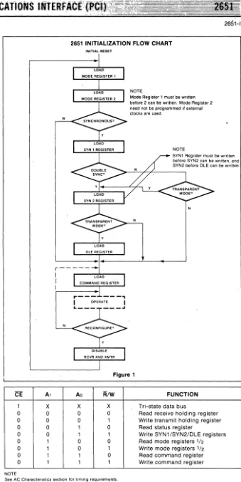
2651 INITIALIZATION FLOW CHART
INITIAL RESET
r--- ---.,
I
I
NOTE
Mode Register 1 must be written before 2 can be written. Mode Register 2 need not be programmed If external clocks are used.
N
N
Figure 1
Ao R/W FUNCTION
X X Tri-state data bus
0 0 Read receive holding register
0 1 Write transmit holding register
1 0 Read status reg ister
2651-1
the mode and command registers. In addi-tion, if synchronous operation is pro-grammed, the appropriate SYN/DLE regis-ters must be loaded. The PCI can be reconfigured at any time during program execution. However, the receiver and trans-mitter should be disabled if the change has an effect on the reception or transmission of a character. A flowchart of the initialization process appears in Figure 1.
0 0 1 1 Write SYN1/SYN2/DLE registers
The internal registers of the PCI are ac-cessed by applying specific signals to the CE, R/W, At and Ao inputs. The conditions NOTE
0 0 0 0 1 1 1 1
0 0
0 1
1 0
1 1
necessary to address each register are See AC Characteristics section for timing requirements.
Read mode registers 1/2
Write mode registers 1/2
[image:25.618.223.562.41.718.2]PRELIMINARY SPECIFICATION
The SYN1, SYN2, and OLE registers are accessed by performing write operations with the conditions A1 =O,Ao= 1, and R/W = 1. The first operation loads the SYN1 regis-ter. The next loads the SYN2 register, and the third loads the OLE register. Reading or loading the mode registers is done in a similar manner. The first write (or read) operation addresses Mode Register 1, and a subsequent operation addresses Mode Reg-ister 2. If more than the required number of accesses are made, the internal sequencer recycles to point at the first register. The pointers are reset to SYN1 Register and Mode Register 1 by a RESET input or by performing a "Read Command Register" operation, but are unaffected by any other read or write operation.
The 2651 register formats are summarized in Tables 5, 6, 7 and 8. Mode Registers 1 and 2 define the general operational charac-teristics of the PCI, while the Command Register controls the operation within this basic frame-work. The PCI indicates its status in the Status Register. These regis-ters are cleared when a RESET input is applied.
Mode Register 1 (MR1)
Table 5 illustrates Mode Register 1. Bits MR11 and MR10 select the communication format and baud rate multiplier. 00 specifies synchronous mode and 1 X multiplier. 1 X, 16X, and 64X multipliers are programmable for asynchronous format. However, the multiplier in asynchronous format applies only if the external clock input option is selected by MR24 or MR25.
MR13 and MR12 select a character length of 5, 6, 7, or 8 bits. The character length does not include the parity bit, if programmed, and does not include the start and stop bits in asynchronous mode.
MR14 controls parity generation. If enabled, a parity bit is added to the transmitted character and the receiver performs a parity check on incoming data. MR15 selects odd or even parity when parity is enabled by MR14.
In asychronous mode, MR17 and MR16 select character framing of 1, 1.5, or 2 stop bits. (If 1 X baud rate is programmed, 1.5 stop bits defaults to 1 stop bits on transmit), In synchronous mode, MR17 controls the number of SYN characters used to establish
2651-1
synchronization and for character fill when the transmitter is idle. SYN1 alone is used if MR17
=
1, and SYN1-SYN2 is used when MR17 = O. If the transparent mode is speci-fied by MR16, OLE-SYN1 is used for char-acter fill, butthe normal synchronization se-quence is used.Mode Register 2 (MR2)
Table 6 illustrates Mode Register 2. MR23, MR22, MR21, and MR20 control the fre-quency of the internal baud rate generator (BPS), Sixteen rates are selectable. When drIven by a 5.0688 MHz input at the BRCLK input (pin 20), the BRG output has zero error except at 134.5, 2000, and 19,200 baud, which have errors of +0.01 0%, +0.235%, and +3.125% respectively. .
MR25 and MR24 select either the BRG or the external inputs TxC and RxC as the clock source for the transmitter and receiver, respectively. If the BRG clock is selected, the baud rate factor in asynchronous mode is 16X regardless of the factor selected by MR11 and MR10. In addition, the corre-sponding clock pin provides an output at 1 X the baud rate.
MR17
J
MR16 MR15 MR14 MR13I
MR12 MR11I
MR10 Parity Type Parity Control Character Length Mode and Baud Rate FactorASYNCH: STOP BIT LENGTH
00 = INVALID 0=000 0= DISABLED 00 = 5 BITS 00 = SYNCHRONOUS 1X RATE 01 = 1 STOP BIT 1 = EVEN 1 = ENABLED 01 = 6 BITS 01 = ASYNCHRONOUS lX RATE 10 = 11/2 STOP BITS 10 = 7 BITS 10 = ASYNCHRONOUS 16X RATE 11 = 2 STOP BITS 11=8BITS 11 = ASYNCHRONOUS 64X RATE
SYNCH: NUMBER SYNCH: TRANS-OF SYN CHAR PARENCY CONTROL
o
= DOUBLE SYN 0= NORMAL 1 = SINGLE SYN 1 = TRANSPARENTNOTE
Baud rate factor ,n asynchronous applies only 'f external clock ,s selected Factor ,s 16X if ,nternal clock is selected. Table 5 MODE REGISTER 1 (MR1)
MR27
I
MR26 MR25 MR24 MR23I
MR22I
MR21I
MR20 Transmitter ReceiverBaud Rate Selection Clock Clock
0= EXTERNAL 0= EXTERNAL 0000 = 50 BAUD 1000 = 1800 BAUD NOT USED 1 = INTERNAL 1 = INTERNAL 0001 = 75 1001 = 2000
0010 = 110 1010 = 2400 0011 = 134.5 1011 = 3600 0100 = 150 1100 = 4800 0101 = 300 1101 = 7200 0110 = 600 1110 = 9600 0111 = 1200 1111 = 19,200
[image:26.613.46.559.391.562.2]PROGRAMMABI F
COMMUNICATIONS
INTERF~CE
(PCI)
PRELIMINARY SPECIFICATION
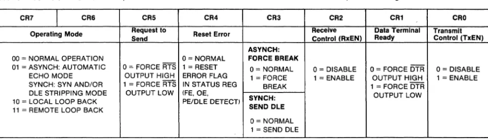
Command Register (CR)
Table 7 illustrates Command Register. Bits CRO (TxEN) and CR2 (RxEN) enable or disable the transmitter and receiver respec-tively. If the transmitter is disabled, it will complete the transmission of the character in the Transmit Shift Register (if any) prior to terminating operation. The TxD output will then remain in the marking state (high!. If the receiver is disabled, it will terminate operation immediately. Any character being assembled will be neglected.
Bits CR1 (DTR) and CRS (RTS) control'l,le DTR and RTS outputs. Data at the outputs is the logical complement of the register data.
In asynchron~)l:s mode, setting CR3 will force and hold the TxD output low (spacing condition) at the end of the current transmit-ted character. Normal operation resumes when CR3 is cleared. The TxD line will go high for a least one bit time before begin-ning transmission of the next character in the Transmit Data Holding Register. In syn-chronous mode, setting CR3 causes the transmission of the DLE register contents prior to sending the character in the Trans-mit Data Holding Register. CR3 should be reset in response to the next TxRDY.
Setting CR4 causes the error flags in the Status Register (SR3, SR4, and SRS) to be cleared. This bit resets automatically.
The PCI can operate in one of four sub-modes within each major mode (synchro-nous or asynchro(synchro-nous!. The operational sub-mode is determined by CR7 and CR6. CR7-CR6
=
00 is the normal mode, with the transmitter and receiver operating inde-pendently in accordance with the Mode and Status Register instructions.In asynchronous mode, CR7-CR6 = 01 places the PCI in the Automatic Echo mode. Clocked, regenerated received data is auto-matically directed to the TxD line while normal receiver operation continues. The receiver must be enabled (CR2
=
1), but theCR7
I
CR6 CR5transmitter need not be enabled. CPU to receiver communications continues nor-mally, but the CPU to transmitter link is disabled. Only the first character of a break condition is echoed. The TxD output will go high until the next valid start is detected. The following conditions are true while in Automatic Echo mode:
1. Data assembled by the receiver is automatically placed in the Transmit HOlding· Register and retransmitted by the transmitter on the TxD output.
2. Transmit clock = receive clock. 3. TxRDY output = 1.
4. The TxEMT/DSCHG pin will reflect only the data set change condition. '
5. The TxEN command (CRO> is ignored.
In synchronous mode, CR7-CR6 = 01 places the PCI in the Automatic SYN/DLE Stripping mode. The exact action taken depends on the setting of bits MR17 and MR16:
1. In the non-transparent, single SYN mode (MR17-MR16 = 10>, characters in the data stream matching SYNl are not transferred to
the Receive Data Holding Register (RHR)' 2. In the non-transparent, double SYN mode
(MR17-MR16 = 00>, characters in the data stream matching SYN1, or SYN2 if immediately preceded by SYN1, are not transferred to the RHR. However, only the first SYNl of an SYN1-SYNl pair is stripped.
3. In transparent mode (MR16 =1), characters in the data stream matching DLE, or SYNl if immediately preceded by DLE, are not trans-ferred to the RHR. However, only the first DLE of a DLE-DLE pair is stripped.
Note that Automatic Stripping mode does not affect the setting of the DLE Detect and SYN Detect status bits (SR3 and SRS!.
Two diagnostic sub-modes can also be configured. In Local Loop Back mode (CR7-CR6 = 10), the following loops are connected internally:
1. The transmitter output is connected to the receiver input.
2. DTR is connected to DCD and RTS is connect-ed to CTS.
CR4 CR3
lalu
2651-1
3. Receive clock = transmit clock.
4. The DTR, RTS and TxD outputs are held high. 5. The CTS, DCD, DSR and RxD inputs are
ig-nored.
Additional requirements to operate in the Local Loop Back mode are that CRO (TxEN), CR1 (DTR), and CRS (RTS) must be set to 1. CR2 (RxEN) is ignored by the PCI.
The second diagnostic mode Is the Remote Loop Back mode (CR7-CR6 = 11!. In this mode:
1. Data assembled by the receiver is automatically placed in the Transmit Holding Register and retransmitted by the transmitter on the TxD output.
2. Transmit clock = receive clock.
3. No data is sent to the local CPU, but the error status conditions (PE, OE, FE) are set. 4. The RxRDY, TxRDY, and TxEMT/DSCHG
out-puts are held high. 5. CRl (TxEN) is ignored.
6. All other signals operate normally.
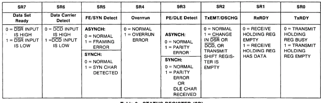
Status Register
The data contained in the Status Register (as shown in Table 8) indicate receiver and transmitter conditions and modem/data set status.
SRO is the Transmitter Ready (TxRDY) sta-tus bit. It, and its corresponding output, are valid only when the transmitter is enabled. If equal to 0, it indicates that the Transmit Data Holding Register has been loaded by the CPU and the data has not been trans-ferred to the Transmit Shift Register. If set equal to 1, it indicates that the Holding Register is ready to accept data from the CPU. This bit is initially set when the Trans-mitter is enabled by CRO, unless a character has previously been loaded into the Holding Register. It is not set when the Automatic Echo or Remote Loop Back modes are programmed. When this bit is set, the TxRDY output pin is low. In the Automatic Echo and Remote Loop Back modes, the output is held high.
CR2 CRl CRD
Operating Mode Request to Reset Error Receive Data Terminal Transmit Send Control fRxEN) Ready Control (TxEN)
ASYNCH: 00 = NORMAL OPERATION 0= NORMAL FORCE BREAK
01 = ASYNCH: AUTOMATIC
o
~ FORCE RTS 1 = RESET 0= NORMAL 0= DISABLE 0= FORCE DTR 0= DISABLE ECHO MODE OUTPUT HIGH ERROR FLAG 1 = FORCE 1 = ENABLE OUTPUT HIGH 1 = ENABLE SYNCH: SYN ANDIOR 1 = FORCERTs IN STATUS REG BREAK 1 = FORCE DTROLE STRIPPING MODE OUTPUT LOW (FE,OE,
SYNCH: OUTPUT LOW 10 = LOCAL LOOP BACK PE/DLE DETECT>
[image:27.617.57.560.577.721.2]PRELIMINARY SPECIFICATION 26!'h-1
SR7 SR6 SR5 SR4 SR3 SR2 SR1 SRO
Data Set Data Carrier FE/SYN Detect Overrrun PE/DLE Detect TxEMT/DSCHG RxRDY
TxRDY
Ready Detect
0= DSR INPUT 0= DCD INPUT ASYNCH: 0= NORMAL 0= NORMAL 0= RECEIVE O=TRANSMIT
IS HIGH IS HIGH 0= NORMAL 1 = OVERRUN ASYNCH: 1 = CHANGE HOLDING REG HOLDING
1 = DSR INPUT 1 =DCD INPUT 1 = FRAMING ERROR 0= NORMAL IN DSR OR EMPTY REG BUSY
IS LOW IS LOW ERROR 1 = PARITY DCD,OR 1 = RECEIVE 1 = TRANSMIT
ERROR' TRANSMIT HOLDING REG HOLDING
SYNCH: SHIFT REGIS- HAS DATA REG EMPTY
0= NORMAL SYNCH: TERIS
1 = SYN CHAR 0= NORMAL EMPTY
DETECTED 1 = PARITY
SR1, the Receiver Ready (RxRDY) status bit, indicates the condition of the Receive Data Holding Register. If set, it indicates that a character has been loaded into the Holding Register from the Receive Shift Reg ister and is ready to be read by the CPU. If equal to zero, there is no new character in the Hold-ing Register. This bit is cleared when the CPU reads the Receive Data Holding Regis-ter or when the receiver is disabled by CR2. When set, the RxRDY output is low.
The TxEMT/DSCHG bit, SR2, when set, indicates either a change of state of the DSR or DCD inputs or that the Transmit Shift Register has completed transmission of a character and no new character has been loaded into the Transmit Data Holding Reg-ister. Note that in synchronous mode this bit will be set even though the appropriate "fill" character is transmitted. It is cleared when the transmitter is enabled by CRO and does not indicate transmitter condition until at
ERROR OR OLE CHAR RECEIVED
Table 8 STATUS REGISTER (SR)
least one character is transmitted. It is also cleared when the Status Register is read by the CPU. When SR2 is set, the TxEMT/-DSCHG output is low.
SR3, when set, indicates a received parity error when parity is enabled by MR14. In synchronous transparent mode (MR16 = 1), with parity disabled, it indicates that a char-acter matching the OLE Register has been received. However, only the first OLE of two successive DLEs will set SR3. This bit is cleared when the receiver is disabled and by the Reset Error command, CR4.
The Overrun Error status bit, SR4, indicates that the previous character loaded into the Receive Holding Register was not read by the CPU at the time a new received charac-ter was transferred into it. This bit is cleared when the receiver is disabled and by the Reset Error command, CR4.
In asynchronous mode, bit SR5 signifies that the received character was not framed by the programmed number of stop bits. (if 1.5 stop bits are programmed, only the first stop bit is checked,) In synchronous non-transparent mode (MR16
=
OJ, it indicates receipt of the SYNl character is single SYN mode or the SYN1-SYN2 pair in double SYN mode. In synchronous transparent mode (MR16=
1), this bit is set upon detection of the initial synchronizing characters (SYNl or SYN1-SYN2) and, after synchronization has been achieved, w~n a DLE-SYNl pair is received. The bit is reset when the receiv-er is disabled, when the Reset Error com-mand is given in asynchronous mode, and when the Status Reg ister is read by the CPU in the synchronous mode.SR6 and SR7 reflect the conditions of the DCD and DSR inputs respectively. A low input sets its corresponding status bit and a high input clears it.
DC ELECTRICAL CHARACTERISTICS
TA = O°C to 70°C, Vee = 5.0V ± 5% 4,5,6LIMITS
PARAMETER TEST CONDITIONS UNIT
Min Typ Max
Input voltage V
VIL Low 0.8
VIH High 2.0
Output voltage V
VOL Low IOL = 1.6mA 0.25
VOH High IOH = -100uA 2.8
IlL Input load current VIN = 0 to 5.5V 10 p.A
Tristate Output leaka'1e current p.A
ILH Data bus high Va = 4.0V 10
ILL Data bus low Va = 0.45V 10
lee Power supply current 90 mA
PRELIMINARY SPECIFICATION
[image:28.617.46.557.87.252.2]