This document contains highly-sensitive confidential information
that may only
be
viewed by employees of Solbourne Computer, Inc.
DO NOT COpy OR DISTRIBUTE THIS MANUAL.
SOLBOURNE COMPUTER, Inc. 1900 Pike Road
Solbourne, Series4lSOO, and Series4lSOO are trademarks of Solboume Computer, Inc
Part Number: l01490-AC
October 1989
Copyright © 1989 by Solbourne Computer, Inc. All rights reserved. No part of this publication may be reproduced, stored in any media or in any type of retrieval system, transmitted in any form (e.g., electronic, mechanical, photocopying, recording> or translated into any language or computer language without the prior written permission of Solbourne Computer, Inc., 1900 Pike Road, Longmont, Colorado 80501. There is no right to reverse engineer, decompile, or disassemble the information contained herein or in the accompanying software.
Solboume Computer, Inc. reserves the right to revise this publication and to make changes from
This manual describes dg, the Solbourne Computer, Inc., standalone/test controller for the Solbourne systems. This manual contains eight sections and three appendices, as follows:
Section 1 - Introduction
This section introduces the Bootable/Standalone Diagnostics program dg.
Section 2 - Getting Started with dg
This section explains how to begin using dg.
Section 3 - Overview of dg Tests
This section presents an overview of the dg tests available.
Section 4 - Memory Tests
The suite of tests for Memory Boards are given in this section.
Section 5 -I/O Tests
The various tests available for the System Board are given in this section.
Section 6 - Graphics Tests
This section presents the tests currently available for Graphics Boards.
Section 7 - Miscellaneous Tests
Miscell~eous tests available under dg are listed in this section.
Section 8 - Commands
This section gives the user commands available when using dg.
Appendix A - MARCH Algorithm
This appendix gives an explaination of how the MARDi algorithm works.
Appendix B - Moving Inversions Test Algorithm
This appendix gives an explaination of how the moving inversions test algorithm works.
Appendix C - Frame Buffer Test Modes
Section 1: Introduction ...•....•...••...•.•... 1-1 1.1 Introduction ...•.••...•... 1-1 1.2 Related Documentation ... 1-1
Section 2: Getting Started with dg ... 2-1 2.1 Introduction ... 2-1 2.2 Invoking the dg Program ... 2-1 2.3 Entering Commands to the dg Prompt ... 2-2 2.4 Using dg Commands ... 2-3 2.4.1 dg Commands ... 2-3 2.5 Starting Test Execution ... 2-4 2.5.1 Using the menu Command ... 2-5 2.5.2 Variations of Test Execution ... 2-8 2.6 Handling Test Failures ... 2-9 2.7 Exiting dg ... 2-10
Section 3: Overview of dg Tests ... 3-1 3.1 Introduction ... 3-1 3.2 Overview of the Menu Structure ... 3-1 3.3 Numerical Test Listing ... 3-4
Section 4: Memory Tests ... 4-1 4.1 Introduction ... 4-1 4.2 Test 1 - Cache Block Virtual Alias Test (affected by prompt) ... 4-1 4.3 Test 2 - Memory Data RAM Test (affected by prompt) ... 4-1 4.4 Test 3 - Memory ECC RAM Test (affected by prompt) ... 4-2
Section 5: System Board Tests ... 5-1 5.1 Introduction ... 5-1 5.2 ASIC Tests ... 5-1 5.2.1 Test 4 - I/O ASIC Register Access Test ... 5-1 5.2.2 Test 5 - I/O ASIC Reset Tests ... 5-2 5.2.3 Test 6 - I/O ASIC FIFO/ECC Test ... 5-3 5.3 LANCE (7990) Tests ... 5-4 5.3.1 Test 7 - 7990 LANCE Initialization Test ... 5-4 5.3.2 Test 8 - 7990 LANCE Internal Loopback Test ... 5-4 5.3.3 Test 9 - 7990 LANCE External Loopback Test (must be prompted) ... 5-5 5.3.4 Test 10 -7990 LANCE Data Alignment Test ... 5-6 5.3.5 Test 11 - 7990 LANCE Cacheable Data Merge Test ... 5-6 5.3.6 Test 12 - 7990 LANCE Address/Cache Data Test (affected by prompt) ... 5-7 5.3.7 Test 13 - 7990 LANCE Cache Block Buswatcher Test ... 5-7 5.4 SCSI (33C93) Tests ... 5-8 5.4.1 Test 14 - 33C93 SBIC (SCSI) Data Path (Write Buffer) Test ... 5-8 5.4.2 Test 15 - SCSI Cacheable Block Data Merge Test ... 5-9 5.4.3 Test 16 - SCSI Multi-bit ECC Error Test ... 5-10
5.4.6 Test 19 - SCSI Cache Block Buswatcher Test •••...•.•....••...•...•. 5-13 5.4.7 Test 20 - SCSI Cache Block Flush Test ... 5-14 5.5 Test 21 - SCSI/LANCE Data 1iansfer Test ....•••••.•..•...•...•...•..•..•....•••••.••..•••••••••••..••...•.... 5-14 5.6 VMEbus Interface Tests ... _... 5-15 5.6.1 Test 22 - VMEbus Address Map RAM Test ... 5-15 5.6.2 Test 23 - VMEbus Data Path Test ... _ •••••..•..•••.•....•... 5-16 5.63 Test 24 - VMEbus Address Path Test .•.•...•••...•.•...•.•...•.•..•••.•...•.•... 5-16 5.6.4 Test 25 - VMEbus Data Multiplexing Test .•....•...•...•... 5-17 5.6.5 Test 26 - VMEbus Interrupt (lACK) Test ... 5-18 5.6.6 Test 27 - RF3500 SCSI Data Path (Write Buffer) Test ... 5-20 5.6.7 Test 28 - VMEbus Cacheable Data Merging Test ... 5-21 5.6.8 Test 29 - VMEbus Block Mode Data Merging Test ... 5-22 5.6.9 Test 30 - VMEbus Cacheable Data Buffer Test ... 5-23 5.6.10 Test 31 - VMEbus Ping-Pong Data Buffers Test ... 5-23 5.6.11 Test 32 - VMEbus Block Mode Address Counter Test ... 5-24 5.6.12 Test 33 - VMEbus Panic Interrupt Test ... 5-24 5.7 BW20 Tests ...•...•...•..•.•..•... 5-25 5.7.1 Test 34 - Frame Buffer RAM Test (affected by prompt) ... 5-25 5.7.2 Test 35 - Frame Buffer Interrupt and Interrupt Registers Test ... 5-26 5.8 Serial Port Tests ... 5-28 5.8.1 Test 36 - Serial Ports Reset Test ... 5-28 5.8.2 Test 37 - Serial Ports Internal Loopback Test ... 5-29 5.8.3 Test 38 - System TUner Test ... 5-29 5.8.4 Test 39 - Profile TUner Test ... 5-30 5.9 Test 40 - RTC-58321 Real Time Clock Test ... 5-31
6.33.4 Test 62 - Single Cursor Pattern RAM Test ... _... 6-22 6.3.3.5 Test 63 -Both Cursors to Single Cursor Pattern RAM Test ... 6-23 6.3.4 Shadow RAM Tests ... _... 6-24 6.3.4.1 Test 64 - Shadow RAM Test ...••... 6-25 6.3.4.2 Test 65 - Shadow RAM to Bt458 Colormap Update Test ... 6-26 635 Frame Buffer RAM Tests ... 6-27 6.3.5.1 Test 66 - Plane Major Mode Test (affected by prompt) ... 6-28 6.35.2 Test 67 - Pixel Major Mode Test (affected by prompt) ... 6-30 6.3.5.3 Test 68 - Pixel Major to Plane Major Test ... 6-31 6.3.6 ROP Tests ... ~... 6-32 6.3.6.1 Registers Tests ... 6-33 6.3.6.1.1 Test 69 - Single Plane Registers Test ... 6-33 6.3.6.1.2 Test 70 - All Planes to Single Plane Registers Test ... 6-34 6.3.6.1.3 Test 71 - BTLA Mode Single Plane Registers Test ... 6-35 6.3.6.1.4 Test 72 - BTLA Mode All Planes to Single Plane Registers Test ... 6-37 6.3.6.2 Mode Tests ... 6-39 6.3.6.2.1 Test 73 - Mode-O Read Access Test ... 6-39 6.3.6.2.2 Test 74 - Mode-l Read Access Test ... 6-40 6.3.6.2.3 Test 75 - Mode-4 Read Access Test ... 6-42 6.3.6.2.4 Test 76 - Mode-5 Read Access Test ... 6-44
6.3.6.2.5 Test 77 - Mode-6 Read Access Test ... 6-45 6.3.6.2.6 Test 78 - Mode-O Write Access Test ... 6-47 6.3.6.2.7 Test 79 - Mode-l Write Access Test ... 6-49 6.3.6.2.8 Test 80 - Mode-2 Write Access Test ... 6-51 6.3.6.2.9 Test 81 - Mode-3 Write Access Test ... 6-53 6.3.6.2.10 Test 82 - Mode-4 Write Access Test ... 6-55 6.3.6.2.11 Test 83 - Mode-5 Write Access Test ... 6-57 6.3.6.2.12 Test 84 - Mode-6 Write Access Test ... 6-59 6.3.6.2.13 Test 85 - Mode-7 Write Access Test ... 6-61 6.3.7 Retrace Interrupts Tests ... 6-63 6.3.7.1 Test 86 - Vertical Retrace Interrupts Test ... 6-63 6.3.7.2 Test 87 - Framecount Register (Counter) Test ... 6-64
6.3.7.3 Test 88 - Retrace/SCC Interrupt Combination Test ... 6-65 6.3.8 Serial Ports Tests ... 6-67 6.3.8.1 Test 89 - Serial Ports Reset Test ... 6-67 6.3.8.2 Test 90 - Serial Ports Loopback Test ... 6-68
Section 7: Miscellaneous Tests ... 7-1 7.1 Introduction ... 7-1 7.2 Test 91 - Random ECC Generation Test (must be prompted) ... 7-1 7.3 Test 92 - Cache Data Bus Test (must be prompted) ... 7-2 7.4 Test 93 - RS-232-C Connector Loopback Test (must be prompted) ... 7-2 75 Test 94 - IDPROM checksum tests (affected by prompt) ... 7-10 7.6 Test 95 - Ethernet TFTPRead Test ... 7-12 7.7 Test 96 - Disk Write/Read Test (affected by prompt) ... 7-13 7.8 Test 97 - Tape Write/Read Test (must be prompted) ... 7-18 7.9 Test 98 - NMI and Test Switch Test (must be prompted) ... 7-22
8.1 Introd uction ... 8-1
Appendix A: MARa-I Algorithm ... _ ... _._ .•.•. _ .. ,_... A-I A.l Introduction ... _... A-l
Appendix B: Moving Inversions Test Algorithm ...•.••..•... B-1 B.l Introduction ... B-1
Figure 3-1.
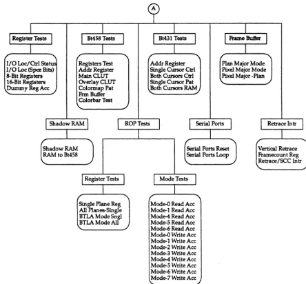
Figure 3-2.
Figure 5-1.
Figure 7-l.
Figure 7-2.
Figure 7-3.
Figure 7-4.
The dg menu Structure ...•...•..•... 3-3
Tests and Test Submenus ... 3-4
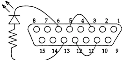
Pin Layout for Transceiver Connector on EXOS 202 ... 5-5
Solbourne Serial Port Loopback Model ... 7-4
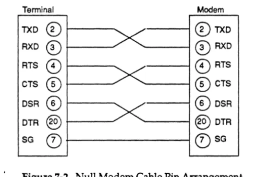
Null Modem Cable Pin Arrangement ... 7-5
Solbourne Serial Port Loopback Model ... 7-8
1.1 Introduction
dg is a standalone test controller for the Solbourne system. This program is used by both manufacturing and field engineering personnel to help detennine which printed circuit board is defective. The primary user of this program is manufacturing.
The software for dg includes:
• The dg standalone/test controller (dg (1»
• Test control commands • Miscellaneous commands • dg tests
1.2 Related Documentation
Information that may be useful while using the dg program is available in the following documentation:
• Series4/600 Service ManUJZl, Part number 101249-AA
• Series4/500 Service ManUJZl, Part number 102161-AA
• Series4/600 Theory ManUJZl, Part number 101250-AA
• Bootable/Standalone Multiprocessor Diagnostics ManUJZl, Part number 101686-AB
• Extended ROM Resident Diagnostics ManUJZl, Part number 101489-AB
2.1 Introduction
This section gives step-by-step instructions and examples for getting started using dg. Additional information on using the tests from the hierarchal menu system of the dg tests is given in Section 3.
In this section, commands you enter are given in boldface type. Command parameters for which you substitute a value are given in italic. Screen output is simulated in constant-width font.
2.2 Invoking the dg Program
The steps to follow the first time dg is invoked are given below.
The user must first bring the Solbourne system to the ROM> prompt. If UNIX is running, it must be shutdown using the halt (1) command.
1. At the ROM> prompt, type:
~
IIt1 -r
IUJ)/i,
f tJ'£
II!)
8 (
t.-. /
1"
ROM> b - f ad.ai ("
6~/atand/dg
dg may also be invoked as follows:
ROM> b - f ad.ai(,,6)~/atand/dg -i file
If -i file is appended to the boot command, the Specified file is opened and dg's internal command buffer is initialized with its contents. For additional information, refer to the fbuf(l) and xbuf(l) commands.
2. When dg is invoked, the following message is displayed:
DG - Standalone Diagnostic Test Controller Version 1.1 August 1, 1989
Copyright (c) 1989 Solbourne Computer, Inc.
Solboume Confidential Information - Do Not Distribute
• The memory configuration table and memory limits are initialized with the values found by the ROM during self-test. (See the eonfig (1) command.)
• The frame buffer configuration table is initialized with the values found by the ROM during self-test and the default frame buffer defaults to the frame. buffer in the highest numbered slot. (See the fbeonfig (1) command.)
• The VMEbus table comes up as empty. (See the vmeeonfig (1) command.)
2.3 Entering Commands to the dg Prompt
dg accepts input when the
DG>
prompt is displayed.
Commands and parameters are case insensitive. Other rules for entering commands include:
1. In general more than one command can be entered in a single command line to the DG>
prompt at the same time.
DG> testa 1 2 3 names on p.sal~ 0 between 5 run
The above command line selects tests 1,2, and 3, turns the printing of test names on, sets the pass limit to 0 (no passlim), the between count is set to 5, and begins test execution with the run command.
~~~NOTE~~~
It is important to remember that error messages from one test are not valid, if failures have occurred during previous tests. The errors from a test must be corrected before advancing to the next test.
2. Commands that process user input in an interactive mode, such as vmeconfig (1) and fbeonfig (1), cause commands that follow on the command line to be ignored.
3. Commands must be separated by white space(s), including tabs or spaces. (Semicolons are not recognized by dg as spaces.)
4. If any of the command(s) entered return an error condition, all following commands are ignored and the DG> prompt is redisplayed.
5. If a command is unrecognized by dg, the following is displayed: Unknown command (command name)
6. All command lines are terminated by a Return.
7. Some commands may display additional error messages if numeric values are entered incorrectly or if the numeric values are not legal. These messages identify the value that is out of range, for example
illegal address (value given)
legal range of values.
8. Memory and I/O addresses and contents must be entered in hexidecirnaI format. Any value that has to do with hardware must also be entered in hexidecirnaI <e.g., register data, memory address, or memory data).
9. Counters and test numbers should be entered in decimal format (e.g., counts and limits). 10. The dg help (1) command can be used any time the DG> prompt is displayed. A
summary of the command given as an argument to help will be displayed.
2.4 Using dg Commands
Example usage of each dg command is given in Section 8 of this manual. All commands can be used with any other commands.
2.4.1 dg Commands
dg command names and their functions follow:
• between (1) -Set or display between count • cd (1) -Change to a different test directory
• config (1) -Generate or display memory configuration file • continue (1) -Set or display continue on error flag
• deposit (1) -Deposit data at specified address • errlim (1) -Set or display error limit
• errors (1) -Display error count
• examine (1) - Examine contents of memory
• fbconfig (1) - Generates (or modifies) the frame buffer configuration file • fbuf (1) - Fill internal command buffer
• help (1) - Display this command list or information on a specific command • limit (1) -Display or set memory test limits
• loop (1) - Set or display loop on test flag • Is (1) - List contents of test directory • menu (1) - Display listing of available tests
• names (1) -Enable or disable printing of test names during test execution • next (1) -Execute next selected test
• passes (1) -Display pass count • passlim (1) -Set or display pass limit • prompt (1) -Set or display prompt flags
Solboume Confidential Information - Do Not Distribute
• quit (1) - Exit from dg debugger program • restart (1) -Restart execution of selected tests • run (1) - Start execution of selected tests
• status (1) -Display or reset state of modes, flags, and counts
• screenload (1) -Loads a raster image file into the specified frame buffer • tests (1) - Select or display tests to be executed
• time (1) -Set or display print time flag and print current date and time • vmeconf (1) - Configure VMEbus devices
• what (1) - Display information about Kbus boards installed in system • xbuf(1) - Load, display, save, or execute the contents of the command buffer
2.5 Starting Test Execution
By default, when dg is invoked all the tests are selected. Tests are executed when the run (1) command is entered at the command line. For example:
DG> run
If the tests command is entered (without an argument, all the selected tests are displayed. For example:
DG> tests
selected tests: 1 2 3 4 5 6 7 8
9 10 11 12 13 14 15 16
17 18 19 20 21 22 23 24
25 26 27 28 29 30 31 32
33 34 35 36 37 38 39 40
41 42 43 44 45 46 47 48
49 50 51 52 53 54 55 56
57 58 59 60 61 62 63 64
65 66 67 68 69 70 71 72
73 74 75 76 77 78 79 80
81 82 83 84 85 86 87 88
89 90 91 92 93 94 95 96
Solboume Comdentiallnformation - Do Not Distribute
The test selection can be modified any time the DC> prompt is displayed by using the tests command. For example:
DG> t •• ts 9 8 .. DG> t •• ts
selected tests: DG>
9
2.5.1 Using the menu Command
8 4
The menu command identifies the test names or their functions. For example:
DG> menu
Menu of installed test programs (-~> denotes menu) : ==> Memory Tests
-==> 10 Tests
==> Graphics Tests -=> Miscellaneous Tests
Displays the top level of the menu directory. The menu command followed by the all argument gives a listing of all the tests and the menu directory in which they reside, as follows:
DG> menu all
Menu of installed test programs (-=> denotes menu) : ==> Memory Tests
1: Cache block virtual alias test (affected by prompt) 2: Memory Data RAM test (affected by prompt)
3: Memory ECC RAM test (affected by prompt) .. => 10 Tests
==> ASIC Tests
4: I/O ASIC register access test 5: I/O ASIC reset tests
6: I/O ASIC FIFO/ECC test -=> LANCE (7990) Tests
7: 7990 LANCE initialization test 8: 7990 LANCE internal loopback test
9: 7990 LANCE external loopback test (must be prompted) 10: 7990 LANCE data alignment test
Solboume Confidential Information - Do Not Distribute
Continued &om previous page
11: 7990 LANCE cacheable data merge test
12: 7990 LANCE address/cache data test (affected by prompt) 13: 7990 LANCE cache block buswatcher test
-=> SCSI (33C93) Tests
14: 33C93 SBIC (SCSI) data path (Write Buffer) test 15: SCSI cacheable block data merge test
16: SCSI Multi-bit ECC error test 17:
18: 19: 20: 21:
SCSI page overflow bit test
SCSI address counter/cache data test SCSI cache block buswatcher test SCSI cache block flush test SCSI/LANCE data transfer test
==> VMEbus interface Tests
22: VMEbus address map RAM test 23: VMEbus data path test
24: VMEbus address path test 25: VMEbus data multiplexing test 26: VMEbus Interrupt (lACK) test
27: RF3500 SCSI data path (Write Buffer) test 28: VMEbus cacheable data merging test
29: VMEbus block mode data merging test 30: VMEbus cacheable data buffer test 31: VMEbus ping-pong data buffers test 32: VMEbus block mode address counter test 33: VMEbus panic interrupt test
-=> BW20 Tests
34: Frame Buffer RAM Test (affected by prompt)
35: Frame Buffer interrupt and Interrupt Registers Tests
-=> Serial Ports Tests
36: Serial ports reset test
37: Serial ports internal loopback test 38: System Timer test
39: Profile Timer test
40: RTC-58321 real time clock test
==> Graphics Tests
==> CG40 Tests
==> Bt458 Tests 41: Registers Test
42: Address Register (Autoincrement) Test 43: Main CLUT (Colormap) Test
44: Overlay CLUT (Colormap) Test
45: Frame Buffer RAM Test (affected by prompt)
46: Frame Buffer Interrupt and Interrupt Registers Tests
Continued &om previous page
--> CG30 Tests
_a> Registers Tests
47: 10 location/control status registers test 48: 10 location (space bits) register test 49: 8-bit registers test
50: 16-bit registers test
51: Dummy registers access test -=> Bt458 Tests
52: Registers test
53: Address register (autoincrement) test 54: Main CLUT (Colormap) test
55: Overlay CLUT (Colormap) test
56: Colormap pattern test (must be prompted) 57: Frame buffer to colormap test
58: Colorbar test pattern (must be prompted) _a> Bt431 Tests
59: Address register (autoincrement) test 60: Single cursor control registers test
61: Both cursors to single cursor control registers test 62: Single cursor pattern RAM test
63: Both cursors to single cursor pattern RAM test -=> Shadow RAM Tests
64: Shadow RAM test
65: Shadow RAM to Bt458 colormap update test -=> Frame Buffer RAM Tests
66: Plane major mode test (affected by prompt) 67: Pixel major mode test (affected by prompt) 68: Pixel major to plane major test
-=> ROP Tests
-=> Registers Tests
69: Single plane registers test
70: All planes to single plane registers test 71: BTLA mode single plane registers test
72: BTLA mode all planes to single plane registers test _a> Mode Tests
73: Mode-O read access test 74: Mode-1 read access test 75: Mode-4 read access test 76: Mode-5 read access test 77: Mode-6 read access test 78: Mode-O write access test 79 : Mode-1 write access test 80: Mode-2 write access test 81: Mode-3 write access test 82: Mode-4 write access test
Solboume Confidential Information - Do Not Distribute
Continued from previous page
83: Mode-5 write access test 84: Mode-6 write access test 85: Mode-7 write access test _a> Retrace Interrupts Tests
86: Vertical retrace interrupts test 87: Framecount register (counter) test 88: Retrace/SCC interrupt combination test _a> Serial Ports Tests
89: Serial ports reset test 90: Serial ports loopback test ==> Miscellaneous Tests
DG>
91: Random ECC generation test (must be prompted) 92: Cache data bus test (must be prompted)
93: RS232 connector loopback test (must be prompted) 94: IDPROM checksum tests (affected by prompt)
95: Ethernet tftp read test
96: Disk write/read test (affected by prompt) 97: Tape write/read test (must be prompted) 98: NMI and Test switch test (must be prompted)
For more information on the hierarchal menu system of dg and test execution, refer to Section 3 and also see the tests (1), run (1), and menu (1) commands in Section 8.
2.5.2 Variations of Test Execution
This subsection discusses some of the basic variations that can be applied to test commands. There are other variations than those given here.
Two results can occur during test execution. The test can pass or the test can fail.
H the test passes, the user may use any of the available dg commands to "customize" the test selection and execution modes, or may exit dg by entering the quit(1) command. The available options to the user include:
• Select other tests for execution
• Tell the controller how many iterations to run using the passlim (1) command followed by
the restart (1) command .
• Controls whether the test names are printed using the names (1) command
• The user can also stop test execution at any time by entering a Control-C rC). Since the tty drivers at the standalone level poll for input there may be a delay between the time the AC is entered and when the test calls the driver routine to check for input. The user should be patient and not repeatedly enter the AC command.
If the test fails, the user can do any of the following:
• Continue the failing test with the run command
• Skip to the next test in the selected sequence of tests using the next (1) command
• Restart the entire sequence using the restart (1) command • Exit dg using the quit command
2.6 Handling Test Failures
Several of the commands given in Section 8 that are used for test control can be used when test failures occur. In the following example, test 1 detects a failure and the loop and quiet commands are used to set up a scope loop.
DG> teata 2 run
Starting Test 2: Cache Block Virtual Alias ~st (affected by prompt)
TEST 2 ERROR: Thu Dec 1 10:03:05 1988
Data error on vaddr Ox10000, paddr Oxff040000 exp
=
Oxff040000act
=
Oxff050000 DG>Note that test 2 has displayed its error message which identified the failing test case and returned to the DG> prompt. If the user wishes to evaluate this test failure by setting up a scope loop, the sequence of commands shown in the following illustration may be entered.
DG> l.oop OD run
TEST 2 ERROR: Thu Dec 1 10:03:05 1988
Data error on vaddr Ox100DO, paddr Oxff040000 exp - Oxff040000
act - Oxff050000 DG>
Solboume Con6.dentiallnformation - Do Not Distribute
DG> quiet on run
(No information is displayed while the test is looping when the quiet command is invoked.)
... c
Test interrupted, type "run" to resume
DG>
No information is displayed while the loop and quiet flags are set. The program is not hung. It is executing in the tightest possible loop of the failing test case. A Control-C must be entered to halt the loop and return to the DG> prompt.
~~~NOTE~~~
It is a common mistake to forget to reset the loop and quiet flags before restarting the test sequence. This causes the first test case in the first test to be executed in a tight loop. See the loop and quiet commands in Section 8 for additional information.
2.7 Exiting dg
3.1 Introduction
This section presents an overview of the dg tests. For instructions on executing tests, refer to Section 2 and the run (1) and tests (1) commands in Section 8.
The infonnation given in this section includes: • An overview of the menu structure • A numerical listing of all dg tests
3.2 Overview of the Menu Structure
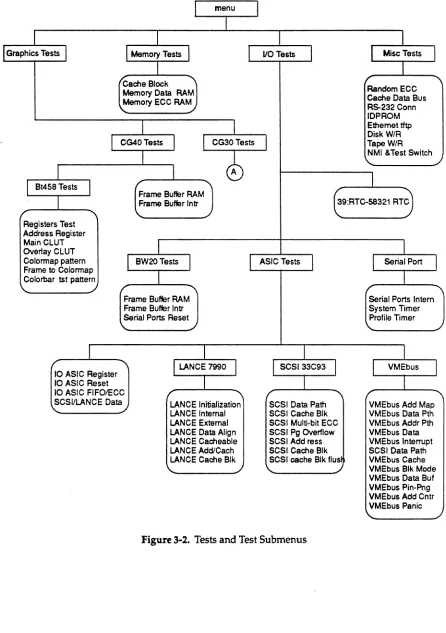
The dg menu of tests is similar to the hierarchal tree-like structure of the UNIX file system. Figure 3-1 illustrates the menu structure of dg.
ASIC Tests
SCSI 33C93
[image:23.615.80.528.337.664.2]Frame Buffer
Solboume Confidential Inlormation - Do Not Distribute
Moving about the dg menu structure has been made easier by the installation of the UNIX-type commands cd (1) and Is (1). Refer to Section 2 and Section 8 for additional information.
menu
I
I
I
I
I
Graphics TestsI
Memory TestsI
I
VOTestsI
I
MiscTestsI
I
I
"Cache Block 'I 'I
Memory Data RAM Random ECC
Cache Data Bus Memory ECC RAM
RS-232 Conn
~
lOP ROM
I
I
Ethernet tftpI
CG40TestsI
I
CG30Tests TapeW/R Disk W/RI
cb
"
NMI &Test Switch ~J
I
I
I
Bt458 TestsI
I
I' ""'I Frame Butler RAM1
E9:RTC-SS321 RTC
I
Frame Butler IntrRegisters Test Address Register Main CLUT
I
I
Overlay CLUT
Colormap pattern BW20Tests
I
I
ASIC TestsI
I
Serial PortI
Frame to ColormapJ
I
Colorbar tst pattern
/ ""'I
Frame Buffer RAM Serial Ports Intern
Frame Buffer Intr System Timer
Serial Ports Reset Profile Timer
"
~I
I
I
I
"\
I
LANCE 7990I
I
SCSI 33C93I
I
VMEbusI
10 ASIC RegisterI
I
I
10 ASIC Reset
10 ASIC FIFOIECC '\ I' ""'I I' ""'I
SCSI/LANCE Data LANCE Initialization SCSI Data Path VMEbus Add Map
~ LANCE Internal SCSI Cache Blk VMEbus Data Pth
LANCE External SCSI Multi-bit ECC VMEbus Addr Pth LANCE Data Align SCSI Pg Overflow VMEbus Data LANCE Cacheable SCSI Add ress VMEbus Interrupt LANCE Add/Cach SCSI Cache Blk SCSI Data Path LANCE Cache Blk SCSI cache Blk flus VMEbus Cache
\.. VMEbus Blk Mode
VMEbus Data Buf VMEbus Pin-Png VMEbus Add Cntr VMEbus Panic
[image:25.612.83.529.98.731.2]Solboume Confidential Information - Do Not Distribute
cy
I
I
I
Register TestsI
I
Bt458 TestsI
I
Bt431 TestsI
I
Frame BuKerI
I
I
/
"'
"\I/O Loc/Ctrl Status Registers Test Addr Register Plan Major Mode I/O Loc (Spce Bits) Addr Register Single Cursor Ctrl Pixel Major Mode 8-Bit Registers MainCLUT Both Cursors Ctrl Pixel Major -Plan 16-Bit Registers Overlay CLUT Single Cursor Pat ./
~yRegAce ./ Colormap Pat Both Cursors RAM./
Frm Buffer Colorbar Test
./
I
Shadow RAMI
I
ROPTestsI
I
Serial PortsI
I
Retrace lntrI
Shadow RAM
I
Serial Ports Reset Vertic::al Retrace RAM to Bt458 Serial Ports Loop Framecount Reg Retrace/SCC lntr\..
I
Register TestsJ
I
ModeTests"'
[image:26.618.89.534.86.498.2]Single Plane Reg Mode-O Read Ace All Planes-Single Mode-l Read Ace BTLA Mode Sngl Mode-4 Read Ace BTLA Mode All Mode-5 Read Ace Mode-6 Read Ace Mode-O Write Ace Mode-l Write Ace Mode-2 Write Ace Mode-3 Write Ace Mode-4 Write Ace Mode-5 Write Ace Mode-6 Write Ace Mode-7 Write Ace \..
Figure 3-2. Tests and Test Submenus (Continued)
3.3 Numerical Test Listing
A numerical listing of all the dg tests is given below. The test number is given on the left side, followed. by the path to the test.
1. memory/Cache block virtual alias test (affected. by prompt) 2. memory/Memory Data RAM test (affected by prompt) 3. memory /Memory ECC RAM test (affected by prompt) 4. 10/ ASIC/I/O ASIC register access test
6. 10/ ASIC/I/O ASIC FIFO/ECC test
7. 10/ ASIC/LANCE 7990/7990 LANCE initialization test 8. 10/ ASIC/LANCE 7990/7990 LANCE intemalloopback test
9. 10/ ASIC/LANCE 7990/7990 LANCE extemalloopback test (must be prompted) 10. 10/ASIC/LANCE 7990/7990 LANCE data alignment test
11. 10/ ASIC/LANCE 7990/7990 LANCE cacheable data merge test
12. 10/ ASIC/LANCE 7990/7990 LANCE address/cache data test (affected by prompt) 13. 10/ ASIC/LANCE 7990/7990 LANCE cache block buswatcher test
14. 10/ASIC/SCSI 33C93/33C93 SBIC (SCSI) data path (Write Buffer) test IS. 10/ ASIC/SCSI 33C93/SCSI cacheable block data merge test
16. 10/ ASIC/SCSI 33C93/SCSI Multi-bit ECC error test 17. 10/ASIC/SCSI 33C93/SCSI page overflow bit test
18. 10/ ASIC/SCSI 33C93/SCSI address counter /cache data test 19. 10/ ASIC/SCSI 33C93/SCSI cache block buswatcher test 20. 10/ ASIC/SCSI 33C93/SCSI cache block flush test 21. 10/ ASIC/SCSI/LANCE data transfer test
22. 10/ ASIC/VMEbus/VMEbus address map RAM test 23. 10/ ASIC/VMEbus/VMEbus data path test
24. IO/ASIC/VMEbus/VMEbusaddresspath test 2S. 10/ ASIC/VMEbus/VMEbus data multiplexing test 26. 10/ ASIC/VMEbus/VMEbus Interrupt (lACK) test
27. 10/ ASIC/VMEbus/RF3S00 SCSI data path (Write Buffer) test 28. 10/ ASIC/VMEbus/VMEbus cacheable data merging test 29. 10/ ASIC/VMEbus/VMEbus block mode data merging test 30. 10/ ASIC/VMEbus/VMEbus cacheable data buffer test 31. 10/ ASIC/VMEbus/VMEbus ping-pong data buffers test 32. 10/ ASIC/VMEbus/VMEbus block mode address counter test 33. 10/ ASIC/VMEbus/VMEbus panic interrupt test
34. 10/BW20/Frame Buffer RAM Test (affected by prompt) 3S. 10/BW20/Frame Buffer interrupt and Interrupt Registers Tests 36. 10 ~fW20/Serial ports reset test
37. 101Serial Port/Serial ports intemalloopback test 38. 10/Serial Port/System Timer test
Solboume Confidential Information - Do Not Distribute
40. IO/RTC-58321 real time clock test 41. Graphics/CG40/BT458/Registers Test
42. Graphics/CG40/BT458/ Address register (autoincrement) test 43. Graphics/CG40/BT458/Main CLUT (colonnap) test
44. Graphics/CG40/BT458/Overlay CLUT (colonnap) test
45. Graphics/CG40/BT458/Colormap pattern test (must be prompted) 46. Graphics/CG40/BT458/Frame buffer to colormap test
47. Graphics/CG40/BT458/Colorbar Test Pattern (must be prompted) 48. Graphics/CG40/Frame Buffer RAM Test (affected by prompt) 49. Graphics/CG40/Frame Buffer Interrupt and Interrupt Registers Tests 50. Graphics/CG30/Register Tests/IO Location/Control Status Registers Test 51. Graphics/CG30/Register Tests/IO location (space bits) register test 52. Graphics/CG30/Register Tests/8-bit registers test
53. Graphics/CG30/Register Tests/l6-bit registers test
54. Graphics/CG30/Register Tests/Dummy registers access test 55. Graphics/CG30/Bt458/Registers test
56. Graphics/CG30/Bt458/ Address register (auto increment) test 57. Graphics/CG30/Bt458/Main CLUT (colormap) test
58. Graphics/CG30/Bt458/Overlay CLUT (colonnap) test 59. Graphics/CG30/Bt431/ Address register (autoincrement) test 60. Graphics/CG30/Bt431/Single cursor control registers test
61. Graphics/CG30/Bt431/Both cursors to single cursor control registers test 62. Graphics/CG30/Bt431/Single cursor pattern RAM test
63. Graphics/CG30/Bt431/Both cursors to single cursor pattern RAM test 64. Graphics/CG30/Shadow RAM/Shadow RAM test
65. Graphics/CG30/Shadow RAM/Shadow RAM to Bt458 colonnap update test 66. Graphics/CG30/Frame Buffer/Plane major mode test (affected by prompt> 67. Graphics/CG30/Frame Buffer/Pixel major mode test (affected by prompt) 68. Graphics/CG30/Frame Buffer/Pixel major to plane major test
69. Graphics/CG30/ROP /Register/Single plane registers test
70. Graphics/CG30/ROP /Register/ All planes to single plane registers test '
~f~
74. Graphics/CG30/ROP/Mode/Mode-l Read access test 7S. Graphics/CG30/ROP /Mode/Mode-4 Read access test 76. Graphics/CG30/ROP /Mode/Mode-S Read access test 77. Graphics/CG30/ROP /Mode/Mode-6 Read access test 78. Graphics/CG30/ROP /Mode/Mode-O Write access test 79. Graphics/CG30/ROP /Mode/Mode-l Write access test 80. Graphics/CG30/ROP /Mode/Mode-2 Write access test 81. Graphics/CG30/ROP /Mode/Mode-3 Write access test 82. Graphics/CG30/ROP /Mode/Mode-4 Write access test 83. Graphics/CG30/ROP /Mode/Mode-S Write access test 84. Graphics/CG30/ROP /Mode/Mode-6 Write access test 8S. Graphics/CG30/ROP /Mode/Mode-7Write access test
·86. Graphics/CG30/Retrace Interrupt/Vertical retrace interrupts test 87. Graphics/CG30/Retrace Interrupt/Framecount register (counter) test 88. Graphics/CG30/Retrace Interrupt/Retrace/SCC interrupt combination test 89. Graphics/CG30/Serial Ports/Serial ports reset test
90. Graphics/CG30/Serial Ports/Serial ports loopback test
91. Miscellaneous/Random ECC generatioI:\ test (must be prompted) 92. Miscellaneous/Cache data bus test (must be prompted)
93. Miscellaneous/RS232 connector loopback test (must be prompted) 94. Miscellaneous/IDPROM checksum test (affected by prompt) 9S. Miscellaneous/Ethernet tftp read test
4.1 Introduction
The dg tests available for memory testing are listed in this section.
4.2 Test 1 - Cache Block Virtual Alias Test (affected
by
prompt)
This test verifies that the virtual cache tags will reference the correct entry in the cache RAMs. This test also verifies that a reference to the same physical location through another virtual . reference is invalidated (i.e., aliases are invalidated).
Data error at vaddr OxlOOOO, paddr Oxff040000 exp ~ Oxff040000
act - Oxff050000
This test performs a series of memory page writes and reads in which all physical page address from XXXXOOOO to xxxxeOOO (hex) are written and read using all combinations of virtual page addresses from XXXXOOOO to xxxxeOOO including FF space addresses.
A write to a physical page using a virtual page address creates a unique physical-to-virtual mapping within the MMU. When the physical page is accessed using a different virtual page address, the MMU must break the existing physical-to-virtual mapping so that a new one may be created. To do this, the MMU performs a "purge" operation in which the cached data block is written back to the physical location in memory and re-read into the cache at the new virtual index. This creates the new physical-ta-virtual mapping.
This test insures that the MMU logic which detects the purge condition is operational and that the data (unique for each physical page) is correctly transferred between the cache and the memory system.
If the prompt flag for this test is set, the test prints out status messages that indicate which physical and logical addresses are being used (however this slows thes execution).
4.3 Test 2 - Memory Data RAM Test (affected
by
prompt)
This test is an extended version of the ROM power-up self-test Addressing and Data Test. The test program performs a MAROi test algorithm to verify the addressing and data paths (see the Appendix A for information on the MAROi test algorithm).
The test program determines the test area from the Kbus memory limit entry in the memory limit table (refer to the limit(l) command to modify the test area).
Solboume Confidential Information - Do Not Distribute
During the read-write-read sequence, the target memory block is cached and checked for correct data. The data in the cache is then complemented and the block is flushed back to memory. The target block is then re-read and verified to contain the complemented data.
Legal error codes for the Data RAM Test are:
• 0x00 -Data fault exception occurred during write of memory with initial data pattern • OxlO - Data fault exception occurred during flush of a memory block on write of memory
with initial data pattern
• Ox20 - Data fault exception occurred on first read of forward pass • OxBO - Data miscompare occurred on first read on forward pass
• 0x30 -Data fault exception occurred during flush of target memory block back to memory during forward pass
• Ox40 - Data fault exception occurred on second read of forward pass
• Oxao -Data miscompare occurred on second read on forward pass • OxSO - Data fault exception occurred on first read of reverse pass • OxeD - Data miscompare occurred on first read on reverse pass
• Ox60 - Data fault exception occurred during flush of target memory block back to memory during reverse pass
• Ox70 - Data fault exception occurred on second read of reverse pass • OxeO - Data miscompare occurred on second read on reverse pass
An example of a Data RAM Test failure follows:
Error occurred in data RAM memory test
Error code - OxeO Virtual addr - Ox00800000
Physical addr
=
OxOOeaOOOO Board slot= 2
A data failure was found in the second read on the reverse pass.exp - Ox55555555 act - Ox5555555d xor - Ox00000008
4.4 Test 3 - Memory ECC RAM Test (affected
by
prompt)
The test is an extended version of the ROM power-up self-test AddreSSing and Data Test. The test program performs a MARCH test algorithm to verify the addressing and data paths (see Appendix A for information on the MARCH test algorithm).
The Error Correction Code (ECC) test uses double word stores and loads to/from memory, the data RAM test uses word.
The total test area is blocked into 8 megabyte (or less) blocks which are tested separately.
During the read-write-read sequence, the target memory block is cached and checked for correct data. The data in the cache is then complemented and the block is flushed back to memory.
The target block is then re-read and verified to contain the complemented data. Legal error oodes for the ECC test are:
• 0x00 -Data fault exception occurred during write of memory with initial data pattern
• OxlO - Data fault exception occurred during flush of a memory block on write of memory with initial data pattern
• Ox20 - Data fault exception occurred on first read of forward pass
• 0xS0 - Data miscompare occurred on high word in first read on forward pass • Ox90 - Data miscompare occurred on low word in first read on forward pass
• Ox30 - Data fault exception occurred during flush of target memory block back to memory during forward pass
• Ox40 - Data fault exception occurred on second read of forward pass
• Oxao -Data miscompare occurred on high word in second read on forward pass • OxbO - Data miscompare occurred on low word in second read on forward pass • 0xS0 - Data fault exception occurred on first read of reverse pass
• OxcO - Data miscompare occurred on high word in first read on reverse pass • OxdO - Data miscompare occurred on low word in first read on reverse pass
• Ox60 - Data fault exception occurred during flush of target memory block back to memory during reverse pass
• Ox70 - Data fault exception occurred on second read of reverse pass
• OxeO - Data miscompare occurred on high word in second read on reverse pass
• 0xf0 -Data miscompare occurred on low word in second read on reverse pass
An example of an ECC test failure follows:
Error occurred in ECC RAM memory test
Error code = Ox40 Virtual addr = OxOOBOOOOO
Physical addr = OxOOeaOOOO Board slot = 2
5.1 Introduction
The dg tests available for System Board are listed in this section.
5.2
ASIC Tests
The following tests verify that the I/O ASIC registers can be accessed by the CPU and that the I/O ASIC can fetch good data from memory.
5.2.1 Test 4 - 110 ASIC Register Access Test
This test verifies that the I/O ASIC will retain data in internal registers and verify the access to the Western Digital (33C93) SCSI Bus Interface Controller (SBIC) and the AMD 7990 Local Area Network Controller for Ethernet (LANCE) chips. Refer to the technical manuals of these devices for additional infonnation.
For each test, the invlid bits are masked before comparing data.
The first part of this test checks all I/O ASIC registers for data retention. Each register has a series of patterns written, read back and verified.
Data error in Ethernet receive address register exp OxOOOOOOOO
act
=
Ox00000040The test continues by verifying that each of the I/O ASIC's five (5) read/write rergisters are unique. The test sequence for this test is as follows:
clear all registers
writing the test register to all ones check all for proper data
write all registers to all ones clear the test register
check all for proper data
Solboume Confidential Information - Do Not Disbibute
Data retention error in test register
test register
=
Ethernet receive address register exp - OxOOOlffffact - OxOOOlffef
In the above example, the test registers did not retain the value written to it.
Addressing error on ASIC
test register - SCSI DMA address register value written
=
OxOOOOOOOOregister modified
=
SCSI control/address register exp ~ Ox00007ffdact
=
OxOOOOOOOOIn the above example, writing to the SCSI DMA address register caused the SCSI control/address register to be modified.
The next two tests verify accessability and data retention of the AMD 7990 LANCE chip and the WD 33C93 SBIC chip. Each device is presented a pattern and read back. The LANCE has a 16 bit data bus and the 33C93 has an 8 bit.
The LANCE test uses CSR1 for the test.
Data retention error in LANCE chip exp so Oxfffe
act
=
OxfefeThe 33C93 test uses the total cylinders, low byte, register for the test.
Data retention error in SCSI chip exp OxOS
act
=
OxOO5.2.2 Test 5 - 110 ASIC Reset Tests
This test verifies the reset circuitry associated with the I/O ASIC. Three resets are available:
2. Reset the 33C93 SCSI Controller 3. Reset the VMEbus
These resets are an address that is strobed. There is a bit for each device to reset. This test verifies that each reset works and that each reset does not cause another reset to occur. (At this time there is no reliable way to verify a VMEbus reset, this portion of the test is bypassed.) The I/O ASIC clears the R/W and prefetch bits in the SCSI control when it is reset. This is the indication that the I/O ASIC has been reset. The I/O ASIC reset is a hardware generated pulse.
Data retention error in ASIC SCSI control register exp - Ox03
act - OxOO
The I/O ASIC reset did not clear by itself.
The ASIC was not reset when reset address was strobed exp OxOO
act
=
Ox03The I/O ASIC reset did not occur.
When reset, the SCSI chip will not load a value into any register. This is the indication that it is reset.
SBIC chip not reset after reset latch set exp ... non zero
act .. OxOO
SBIC chip reset after reset latch reset or data error exp .. OxOO
act
=
OxffPlease refer to the I/O ASIC Specification manual, the 33C93 Technical Reference for further information.
5.2.3 Test 6 -
VO
ASIC FIFOIECC Test
This test verifies the I/O ASIC will fetch a cache block from Kbus memory and that single bit errors in any cacheline will be corrected. Every data bit in every cache line is verified to be correctable. The test verifies the following conditions:
Solboume Confidential Information - Do Not Distribute
4. A zero bit corrected to a one in a field of ones
The LANCE chip is used to force the I/O ASIC to fetch the test cache block.
The cache block is written to memory with one cache line with bad data and good ECC. The I/O ASIC is forced to fetch the block and the cache block is read again. The data read is verified to be corrected.
I/O ASIC FIFO/ECC error check byte - OxOc
addr exp
OxOOOeOOOO OxOOOOOOOOOOOOOOOO
act Ox0000000080000000
xor
Ox0000000080000000
In the above example, the I/O ASIC did not correct the bad bit in the cache line or it did not fetch the block.
5.3 LANCE (7990) Tests
The following tests verify that the AMD7990 LANCE chip and the interface between the LANCE and the I/O ASIC are functional.
5.3.1 Test 7 - 7990 LANCE Initialization Test
This test verifies that the AMD 7990 LANCE chip can initialize through the I/O ASIC from Kbus memory. To verify the initialization, the LANCE status register is verified to contain the expected status.
Ignored bits are masked off.
LANCE initialization error exp status
=
Ox0020 act status = Ox0030 mode value = Ox0002In the above example, the LANCE chip received the wrong mode value. Refer to the AMD 7990 technical manual for further information.
5.3.2 Test 8 - 7990 LANCE Internal Loopback Test
up a transmit packet of 32 bytes, the maximum for the LANCE, and transmits it to itself. The received packet is then verified.
The expected vector for the LANCE chip is Ox87.Interrupts are checked for valid on: 1. Initialization
2. Transmit packet 3. Receive packet
Unexpected interrupt active after LANCE initialization No interrupts expected
vector received K OxBO
In the above example, a device that is not being tested generated an interrupt when the LANCE did something.
Data error on internal LANCE loopback
addr exp act
OxOOOcOOcO Ox0001020304050607 OxOOOl 020384 050607
xor
OxOOOOOOOOBOOOOOOO
In the above example, a bad bit was found in the I/O ASICs' Ethernet cacheable block buffer.
5.3.3 Test 9 - 7990 LANCE External Loopback Test (must be prompted)
This test verifies the operation of the LANCE chip with the data encoding component's on the System Board.
[image:39.615.195.397.510.610.2]An externalloopback connector must be installed before this test is run. Figure 3-3 shows the pin layout for the transceiver connector.
Solboume Confidential Information - Do Not Distribute
Time out on LANCE transmit LANCE status - Ox0033
In the above example, the external loopback connector is not connected or an external component is bad.
5.3.4 Test 10 - 7990 LANCE Data Alignment Test
This test verifies that the I/O ASIC/LANCE interface will transfer different byte counts correctly. This verifies the SE bus data multiplexer in the ASIC for proper operation.
Data error on internal LANCE loopback
addr exp act
OxOOOcOOc8 Ox0855555555555555 Ox0055555555555555
xor Ox0800000000000000
In the above example, the I/O ASIC got a single byte transfer from the wrong side of the SEbus. Please refer to the I/O ASIC Specification Manual and the AMD Local Area Network Controller Am7990 (Lance) Technical Manual for further information.
5.3.5 Test 11- 7990 LANCE Cacheable Data Merge Test
This test verifies the I/O ASIC function of merging new data with existing data when the new data does not start on a 32 byte (cache block) boundary.
The test begins by initializing the test cache block with a known pattern. The test does an internalloopback of 8 bytes (all zeroes) into the prepared cache block at a known offset. Since the LANCE appends 4 byte of EeC to the data, these bytes are expected. The cache block is verified to contain the 8 bytes of zeroes and that none of the other bytes were modified. This procedure is repeated for every 16 bit word position in a cache block (14).
ASIC/LANCE addr OxffOf0180 OxffOf0188 OxffOf0190 OxffOf0198
data merging error exp OxfffeOOOOOOOOOOOO OxOOOOf5f4f3f2flfO Oxefeeedecebeaege8 Oxe7e6e5e4e3e2eleO act OxOOOOOOOOOOOOOOOO OxOOOOOOOOOOOOOOOO OxOOOOOOOOOOOOOOOO OxOOOOOOOOOOOOOOOO xor OxfffeOOOOOOOOOOOO OxOOOOf5f4f3f2flfO Oxefeeedecebeaege8 Oxe7e6e5e4e3e2eleO
Refer to the Kbus Specification Manual, I/O ASIC Specification Manual, and AMD Local Area Network Controller Am7990 (LANCE) Technical Manual for further information.
5.3.6 Test 12 - 7990 LANCE Address/Cache Data Test (affected
by
prompt>
This test verifies the operation and selection of the
I/O
ASIC/LANCE interface transmit registers (TXt and TX2) and verifies the data integrity of the LANCE cache block buffer. The test verifies that:t.
TX address registers are unique and do not interact2. The value in the TX address registers is presented correctly 3. The LANCE cache block buffer has no data failures
The LANCE is set up with 2 receive descriptors/buffers and 2 transmit descriptors/buffers, one uses TXt, the other TX2.
The test starts with TX2 pointing to a fixed transmit buffer and TXt to a moving buffer. Psuedo random data is set into the buffer for TXt and the TX2 data buffer is set to zero. An internal loopback is done using TXt. The data is verified, and the receive buffer is returned to the LANCE. A loopback is then done with TX2 using random data and TXt zero, the data checked and buffer returned. This procedure is repeated using TX2 pointing to the moving buffer and
TXt the fixed.
The moving buffers address is updated, checked for valid and the procedure is repeated until all test addresses are complete.
If this test is prompted, the address increments in the valid range, else the address is taken from a pattern table.
Data error in LANCE cache block
addr exp act
OxOOfcOOcO Ox43856bc2d88ef179 Ox438d6bc2d88ef179
xor Ox0008000000000000
In the above example, the I/O ASIC has a bad bit in the LANCE cache buffer. The I/O ASIC used wrong TX buffer on transmit. The I/O ASIC transmitted a packet using the wrong TX
address register.
Please refer to the Kbus Specification Manual, the I/O ASIC Specification Manual, the AMD Local Area Network Controller Am7990 (Lance) Technical Manual for further information.
5.3.7 Test 13 - 7990 LANCE Cache Block Buswatcher Test
This test verifies the operation of the LANCE interface cacheable buffer buswatcher.
Solboume Confidential Information - Do Not Distribute
H the I/O ASIC provides the data, it will be corrected. H memory supplies it, it will not be corrected. The corrected data is all OO's.
The test is repeated for each test address.
I/O ASIC/LANCE buswatcher error addr
OxOOff9000
exp
OxOOOOOOOOOOOOOOOO
act
Ox0800000000000000
xor
Ox0800000000000000
In the above example, the I/O ASIC did not supply the data when it was read.
Please refer to the Kbus Specification Manual, the I/O ASIC Specification Manual, the AMD Local Area Network Controller Am7990 (Lince) Technical Manual for further information.
5.4 SCSI (33C93) Tests
The following tests verify that the Western Digital 33C93 chips and the interface between the SBIC and I/O ASIC are functional.
5.4.1 Test 14 - 33C93 SBIC (SCSI) Data Path (Write Buffer) Test
This test verifies the operation of the WD 33C93 SBIC chip (SCSI) with the I/O ASIC.
The chip is set with a SCSI id of 7 (highest priority) and interrupts are verified to occur and be the correct vector.
The test sequence is as follows:
• The test waits for a minimum of 5 seconds to allow the device to recover from the SCSI bus reset.
• The test performs a SCSI TEST UNIT READY command. This first command will fail with a check condition status and a sense key of Ox06. This error is expected and accounted for, it is the drive saying it was reset.
• The data to transfer to the device is set up, an incrementing pattern of 512 bytes is used. • The data is transferrecI to the
devic~
using the ScsI WRITE BUFFER command.• The data is transferred from the device using the SCSI READ BUFFER command. • The data read is verified to be the same data that was sent.
SCSI transfer error
addr exp
OxOOOcOOOO Ox00010203040S0607
act Ox00010203840S0607
xor Ox0000000080000000
The ''Timeout on access to target 0 after reset" error specifes that SCSI device address 0 and Logical Unit Number (LUN) 0 could not be selected. Verify the device:
1. Cables are not damaged and connected 2. Is addressed as device 0
3. Is addressed as LUN 0
SCSI errors return the command that was issued. The commands used are:
description command OxOO Ox3b Ox3c device OxOO OxOO OxOO
SCSI command, TEST UNIT READY SCSI command, WRITE BUFFER SCSI command, READ BUFFER
Errors returned from the device will display: 1. SCSI status
2. Target status 3. Command phase
4. SBIC chips status (auxilliary status)
For example:
SCSI status exp ... Ox02 act 0= Ox02
target status Ox02 Ox02 command phase Ox02 Ox02 auxilliary status Ox02 Ox02
Please refer to the 33C93 Technical Reference and the Small Computer Systems Interface (SCSI)
specification for further information.
5.4.2 Test 15 - SCSI Cacheable Block Data Merge Test
Solboume Confidential Information - Do Not Distribute
The test begins by initializing the test cache block with a known pattern. The test reads one zero byte from the device buffer into the prepared cache block at a known offset. The cache block is verified to contain the zero byte and that none of the other bytes were modified. This procedure is repeated for every byte position in a cache block (31). .
iSCSI cache addr
pxffOfOOOO OxffOf0008 OxffOf0010 OxffOf0018
block merge error exp OxffOOfdfcfbfaf9f8 Oxf7f6f5f4f3f2flfO Oxefeeedecebeaege8 Oxe7e6e5e4e3e2eleO act OxOOOOOOOOOOOOOOOO OxOOOOOOOOOOOOOOOO OxOOOOOOOOOOOOOOOO OxOOOOOOOOOOOOOOOO xor OxffOOfdfcfbfaf9f8 Oxf7f6f5f4f3f2flfO Oxefeeedecebeaege8 Oxe7e6e5e4e3e2eleO
In the above example, the I/O ASIC did not merge the data in RAM, but rather used what was already in the cacheable buffer.
Please refer to the Kbus Specification Manual, I/O ASIC Specification Manual, 33C93 Technical Reference, and the Small Computer Systems Interface (SCSI) Specification for further information.
5.4.3 Test 16 - SCSI Multi-bit ECC Error Test
This test verifies the operation of the I/O ASIC when a multi-bit ECC error in ram is detected. The five areas verified are:
1. The I/O ASIC will detect a multi-bit ECC error
2. The I/O ASIC will set the scsi_err bit in the interrupt status register
3. The I/O ASIC will continue to fetch the block and set the scsCerr bit when a zero is written to the scsCerr bit
4. The I/O ASIC will reset the scsCerr bit when a new address is written
5. The I/O ASIC will reset the scsCerr bit when the multi-bit error condition in the cache block referenced has been cleared
The test begins by setting up a cache block with a multi-bit ECC error. A write to the SCSI device is attempted using the address of the error block. Operations 1 - 4 above are verified. The test is repeated to verify operation 5.
SCSI ECC error was not reset by re-writing address
In the above example, the I/O ASIC did not clear the error when the address register was set to a good cache block in memory.
In the above example, the I/O ASIC did not clear the error when good data was written to the test cache block.
Refer to the Kbus Specification Manual, the I/O ASIC Specification manual, the 33C93 Technical Reference and the the Small Computer Systems Interface (SCSI) specification for further information.
5.4.4 Test 17 - SCSI Page Overflow Bit Test
This test verifies the I/O ASIC function halting a SCSI transfer when the transfer crosses a system page address boundary (every 8192 bytes).
The test verifies that during a SCSI read operation the I/O ASIC will: • Stop at the page boundary
• Hold off the SCSI chip transfer, the transfer did not complete • The address register contains the correct value
• The page_overflow bit in the status register is set • A page overflow interrupt is generated
• Data in the next system page is not modified
The test verifies that during a SCSI write operation the I/O ASIC will: • Stop at the page boundary
• Hold off the SCSI chip transfer, the transfer did not complete • The address register contains the correct value
• The page_overflow bit in the status register is set • A page overflow interrupt is generated
The read test writes 8K of zeroes to the devices buffer and sets a byte of Oxff to the first byte of the next page. The test then reads 8K bytes and sets the address to system page boundary + 4K. The read is then started and a timeout is set. When the I/O ASIC encounters a page boundary, all conditions listed above are verified and the read is allowed to complete.
The write test sets the address to system page boundary + 4K. The write is then started and a timeout is set. When the I/O ASIC encounters a page boundary, all conditions listed above are verified and the write is allowed to complete.
SCSI read completed with page overflow active
In the above example, the I/O ASIC flagged the overflow but did not stop the write to memory.
Solboume Confidential Information - Do Not Distribute
In the above example, the I/O ASIC did not detect the page overflow condition.
Ttmeout on page overflow interrupt
In the above example, the I/O ASIC did not interrupt the processor on a page overflow condition.
Unexpected vector after page overflow on read exp
=
Ox83act .. Ox87
In the above example, the I/O ASIC is interrupting on the wrong line or there is a failure on the System Board.
Page overflow did not prevent write to next page exp Oxff
act c OxOO
In the above example, the I/O ASIC did not prevent a write to the next address on a page overflow.
Address miscompare after a page overflow on read exp c OxOOOflfff
act ... OxOOOf2000
In the above example, the SCSI address incrementor in the I/O ASIC is bad. Page overflow bit active after clear on read
In the above example, the I/O ASIC did not clear the overflow bit after the write completed.
Write to memory did not complete after a page overflowO)i exp ... OxOO
act
=
OxffSCSI write completed with page overflow activeO);
In the above example, the I/O ASIC flagged the page overflow but did not stop on the condition.
SCSI write completed without page overflow active
In the above example, the I/O ASIC did not stop on a page overflow condition.
Time out on SCSI write after a page overflow page overflow bit inactive
In the above example, the I/O ASIC did not continue the transfer when a new address was written, if the page overflow bit is "active," the I/O ASIC did not clear the bit.
Page overflow bit active after clear on write
In the above example, the I/O ASIC did not clear the overflow bit after the write completed. Please refer to the Kbus Specification Manual, I/O ASIC Specification Manual, and WD 33C93 SBIC Technical Manual for further information.
5.4.5 Test 18 - SCSI Address Counter/Cache Data Test
This test verifies the operation of the SCSI address counter and checks the SCSI cache block buffer for data errors. The test is a write/read loop to/from the SCSI devices buffer.
The test writes and reads 8192 bytes of data to the SCSI devices buffer on each pass. The data used is random and the data is checked after every read. Data errors may be from address or cache buffer faults.
Please refer to the Kbus Specification Milnual, the I/O ASIC Specification Manual, and the WD
33C93 SBIC Technical Milnual for further information.
5.4.6 Test 19 - SCSI Cache Block Buswatcher Test
This test verifies the operation of the SCSI interface cacheable buffer buswatcher.
Solbourne Confidential Information - Do Not Distribute
again.
If the I/O ASIC provides the data, the data will be corrected. If memory supplies it, it will not be corrected. The corrected data is all OO's.
The test is repeated for each test address.
I/O ASIC/SCSI buswatcher error addr
OxOOffeOOO
exp
OxOOOOOOOOOOOOOOOO
act
Ox0800000000000000
xor
Ox0800000000000000
In the above example, the I/O ASIC did not supply the data when it was read.
Please refer to the Kbus Specification Manual, the I/O ASIC Specification Manual, and the WD 33C93 SBIC Technical Manual for further information.
5.4.7 Test 20 - SCSI Cache Block Flush Test
This test verifies the operation of the SCSI interface cacheable buffer flush when the flush address is strobed.
The test begins by writing a known pattern to the SCSI device. The data is then read back with the last byte being written to the first byte of the cache block buffer. The SCSI address register is set to the next to last byte of the cache block. The SCSI flush address is strobed and the test data is verified to be correct.
The test is repeated for each byte offset in the cache block 0-31).
SCSI cache flush error bytes into cache block
=
1addr exp
OxOOffeOOO Oxc300000000000000
act
OxOOOOOOOOOOOOOOOO
xor
Oxc300000000000000
In the above example, the I/O ASIC did not flush the data when the flush address was strobed. Please refer to the Kbus Specification Manual, the I/O ASIC Specification Manual, and the WD 33C93 SBIC Technical Manual for further information.
5.5 Test 21 - SCSIILANCE Data Transfer Test
This test verifies the operation of the I/O ASIC when the SCSI and LANCE devices are running at the same time.
If the test is prompted, the number of SCSI write/reads before a data check is wanted and the number of data check iterations wanted is asked for. Entering "c(' or "(1' to any of these prompts exits the test. The test defaults to 10 for each loop.
Please refer to the Kbus Specifiaztion Manual, the I/O ASIC Specification Manual, the WD 33C93 SBIC Technical Manual, and the AMD Local Area Network Controller Am7990 (lAnce) Technical Manual for further information.
5.6 VMEbus Interface Tests
The following tests verify that the VMEbus interface on the System Board is functional. This includes tests for the I/O ASIC VMEbus port, the VMEbus address map, and the ability to run VMEbus cycles. Some of the tests in this subsection require VMEbus boards to be installed. Refer to the test descriptions and the vmeconfig command to find the command to be used to enable them.
5.6.1 Test 22 - VMEbus Address Map RAM Test
This test verifies that the VMEbus address map RAM on the System Board is accessible via RIO transactions. It does not verify that Kbus/VMEbus address translations can be performed. The VMEbus map RAM is a 2048 word memory and is accessible at low address 83000000 and high address 83ffeOOO. The adjacent locations in the RAM are at 2000 hexadecimal increments. Currently, each RAM location is 32 bits. However, only four buts can be read. This test only checks four bits from each location in the RAM.
Strategy: Write random byte sequence to 2048 VMEbus map RAM locations. Read and verify contents of VMEbus map RAM.
Possible error messages follow:
VMEbus address map write/read error
RIO address
=
OxYYYYYYYY exp .. EEEEEEEEact = AAAAAAAA xor .. XXXXXXXX
where:
YYYYYYYY - RIO address where error occurred
EEEEEEEE - value expected to be read from address AAAAAAAA - actual value read from address
XXXXXXXX - xor of expected and actual values
If this test fails, the control logic for accessing the RAM should be checked to be functional. If
Solboume Confidential Information - Do Not Distribute
5.6.2 Test 23 - VMEbus Data Path Test
This test verifies correct data path access to the VMEbus using RIO cycles. This test requires a VMEbus Memory Board installed in the VMEbus backplane and the boards' presence listed in the VMEbus configuration table (see the command 'vmeconfig' for more information).
The test program writes and reads the VMEbus RAM board as a 16 bit device and an 8 bit device. The 8 bit device test verifies that the correct VMEbus data strobe line is used and that
the unused data strobe does not. The test is run for each data strobe line.
VMEbus data error, 16 bit accesses address - Ox86100000
act - Oxfffe exp ... Oxffff xor ... OxOOOl
VMEbus data error, 8 bit accesses address
=
Ox86100000act
=
Oxff02 exp - OxffOO xor ... Ox00025.6.3 Test 24 - VMEbus Address Path Test
This test verifies that address lines on the VMEbus backplane do not interact with each other. This test requires a VMEbus Memory Board installed in the VMEbus backplane and the boards' presence listed in the VMEbus configuration table (see the vmeconfig-(1) command for more information).
The test writes and reads the VMEbus RAM board as a 16 bit device. The test program sets the entire VMEbus RAM to OXOOOO, then each single bit address line is set to Oxffff. For example:
address contents
OxOOOOOO OxOOOO
OxOOOOO2 Oxffff
OxOOOOO4 Oxffff
OxOOOOO6 OxOOOO
OxOOOOO8 Oxffff
OxOOOOOa OxOOOO
OxOOOOOc OxOOOO
OxOOOOOe OxOOOO
OxOOOO1O Oxffff
OxOOOO12 OxOOOO
In this way any address line that interacts with another one will write the opposite data to the location.
The test is repeated using a single low bit in the address.
VMEbus addressing error address = Ox86100000 act
=
Oxffffexp - OxOOOO
5.6.4 Test 25 - VMEbus Data Multiplexing Test
This test verifies the RIO data mutiplexing of the I/O ASIC to the VMEbus. It ensures the data going to any VMEbus device or ram will be presented in the correct position and without error. This test requires a VMEbus ram board to be installed and configured (see command 'vmeconf' for further information) before this test will run.
The first part of this test is a simple data path check, verifying the 32 bit data path. This check is made to both positions of the 64 bit Kbus data path. After the 32 bit path is known to work, the 16 and 8 bit transfers are done using 32 bit transfers