ISSN Online: 1947-3818 ISSN Print: 1949-243X
Design and Implementation of a Three-Phase
Active T-Type NPC Inverter for
Low-Voltage Microgrids
Rick Chen
1, Ying-Yu Tzou
21AcBel Polytech Inc., Taiwan
2Institute of Electrical Control Engineering, National Chiao Tung University, Taiwan
Abstract
This paper presents the design and implementation of a 3 kVA three-phase active T-type neutral-point clamped (NPC) inverter with GaN power devices for low-voltage microgrids. The designed inverter is used in a battery-based energy system (BESS) for power conversion optimization in applications to low-voltage microgrids. A modular design method has been developed for the design and implementation of the AT-NPC inverter. Experimental verifica-tion has been carried out based on a 3-kW three-phase T-Type NPC grid- connected inverter. FPGA based digital control technique has been developed for the current control of the three-level three-phase grid inverter. A maxi-mum efficiency of 98.49% has been achieved within a load range from 50% to 75%.
Keywords
Active T-Type NPC Inverter, Modular Design Methodology, Loss Analysis, Efficiency Optimization
1. Introduction
Multi-level converters (MLC) have been traditionally adopted for static power conversion and motor drives in medium voltage applications [1] [2]. Although various converter topologies have been developed for medium voltage applica-tions, the three-level neutral-point clamped (NPC) converter topology is the most frequently selected for industrial applications due to its advantages of sim-plicity and reliability [3] [4] [5]. With the advances of modularized power devic-es developed for the implementation of active T-type NPC inverters [6] [7] [8] [9], AT-NPC inverters are becoming a competitive choice for PV inverters and How to cite this paper: Chen, R. and Tzou,
Y.-Y. (2017) Design and Implementation of a Three-Phase Active T-Type NPC Inverter for Low-Voltage Microgrids. Energy and Power Engineering, 9, 70-77.
https://doi.org/10.4236/epe.2017.94B009
motor drives in low voltage applications [10]-[15].
2. T-Type NPC Inverter
The 3-level active T-type NPC inverter, as show in Figure 1(b), provides an ad-ditional middle point of its DC-link voltage for its voltage switching, and thus the inverter voltage is reduced to half compared with the conventional 2-level inverter as shown in Figure 1(a). The reduction of voltage switching level pro-vides advantages such as lower switching losses, smaller filters for both the dc-link capacitor and output filters, lower EMI and leakage current, higher power density with improved efficiency.
The drawbacks of the AT-NPC inverters are extra AC switches with their cor-responding isolated gate drives are required, more sophisticated PWM strategy and balancing control scheme are required. However, with the development of new generation wide bandgap (WBG) semiconductors such as Gallium Nitride (GaN) and Silicon Carbide (SiC), and the high-performance advanced FPGA embedded microprocessors, an active T-type inverter phase leg may become a standard power module for the implementation of an idea renewable power conversion system.
Vertical GaN devices provide advantages such as high voltage blocking capa-bility, very low conduction resistance with very small footprint, and high oper-ating temperature, but still exists a major challenge for reliable mass production.
(a)
[image:2.595.216.537.405.714.2](b)
On the other hand, lateral GaN-on-Si devices are a promising alternative. A High-electron-mobility transistor (HEMT), also known as heterostructure FET (HFET), is a field-effect transistor incorporating a junction between two mate-rials with different band gaps. GaN HEMT power devices can achieve low on- state resistance and high-speed switching performance, and provides a possibili-ty to miniaturize the connected power filter components with sophisticated dig-ital control techniques [16]-[21].
3. Implementation and Experimental Results
Practical implementation issues of the AT-NPC inverters using advanced WBG power semiconductor devices have got attentions in recent years [22] [23]. There still left many design and implementation issues for the integrated design and control of the AT-NPC inverters with innovative power semiconductor devices and advanced SOPC control technologies. This paper presents the design and implementation of a 3 kW three-phase 3-L AT-NPC inverter using the GaN HEMT power semiconductor devices from Transform. Table 1 gives some key parameters of the designed inverter.
An FPGA-based predictive control scheme has been developed for the current control and efficiency optimization of the designed three-phase T-type NPC grid-tied inverter. T-type inverter has the features of low conduction losses, low switching losses and superior output waveform quality. These benefits will be-come significant as the switching frequency decreases. The proposed control scheme is very promising for high power applications. The 3LT2C basically combines the advantages of the 2-level converter such as low conduction losses and small part count with the advantages of the 3-level converter such as low switching losses and superior output voltage quality.
[image:3.595.210.538.600.734.2]We adopt a modular design method for the design and implementation of the AT-NPC inverter. The converter is designed with a half-bridge AT-NPC inverter as a basic power module. A basic power module includes its own input and out-put filter, gate drive circuits, protection circuits, sensing and control interface circuits, and a local FPGA-based current controller. Other converters can be constructed with several basic AT-NPC modules. Figure 2 shows the modula-rized grid converter design methodology.
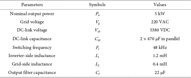
Table 1. Parameters of the constructed 3L AT-NPC inverter.
Parameters Symbols Values
Nominal output power Pn 5 kW
Grid voltage Vg 220 VAC
DC-link voltage Vdc 5380 VDC
DC-link capacitance Cdc 2 × 470 μF in parallel
Switching frequency Fs 48 kHz
Inverter-side inductance L1 1.2 mH
Grid-side inductance L2 0.4 mH
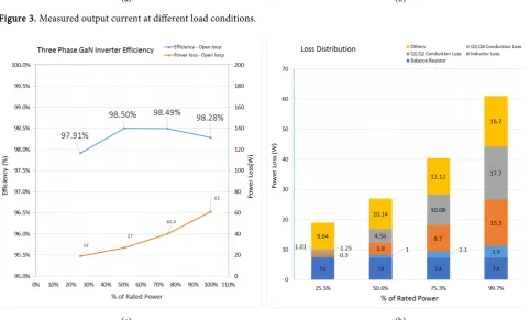
Loss model based on a defined switching waveforms and device characteristics can be used for the efficiency analysis of inverters [24] [25] [26]. The inverter is designed to be operated with a wide range of adjustable switching frequencies from 3 kHz to 60 kHz. Figure 3 shows the experimental results of measured output current of the designed 3 L AT-NPC inverter at different loading condi-tions. Figure 4 shows the measured efficiency and loss distribution as functions of load. A maximum efficiency of 98.49 has been achieved within a load range from 50% to 75%.
[image:5.595.63.539.222.588.2] [image:5.595.58.541.420.711.2](a) (b) Figure 3. Measured output current at different load conditions.
Efficiency optimization with adjustable switching frequency and adjustable DC-link voltage can be carried out with a programmable FPGA-based inverter controller. The designed inverter is tested with a nominal switching frequency of 48 kHz. Efficiency performance measures are functions of load current, switch-ing frequency, and dc-link voltage. For the selected power devices, conduction loss plays a dominant role for ratings above 70%. Experimental results suggest that an efficiency optimization strategy is required to reduce the conduction losses above a specific load ratio while to reduce the switching losses when the load is lower than this specific load ratio.
4. Conclusion
This paper has presented the design and implementation of a 3 kVA three-phase active T-type neutral-point clamped (NPC) inverter with GaN HEMT power de-vices for low-voltage microgrids. For the selected power dede-vices, conduction loss plays a dominant role for ratings above 70%. Experimental results suggest that an efficiency optimization strategy is required to reduce the conduction losses above a specific load ratio while to reduce the switching losses when the load is lower than this specific load ratio. A maximum efficiency of 98.49% has been achieved within a load range from 50% to 75%.
References
[1] Nabae, A., Takahashi, I. and Akagi, H. (1981) A New Neutral-Point-Clamped PWM Inverter. IEEE Trans. Ind. Appl., 17, 518-523.
https://doi.org/10.1109/TIA.1981.4503992
[2] Franquelo, L.G., Rodriguez, J., Leon, J.I., Kouro, S., Portillo, R. and Prats, M.A.M. (2008) The Age of Multilevel Converters Arrives. IEEE Ind. Electron. Mag., 2, 28-39. https://doi.org/10.1109/MIE.2008.923519
[3] Rodriguez, J., Bernet, S., Wu, B., Pontt, J.O. and Kouro, S. (2007) Multi-Level Vol-tage-Source-Converter Topologies for Industrial Medium-Voltage Drives. IEEE Trans. Ind. Electron., 54, 2930-2945.https://doi.org/10.1109/TIE.2007.907044
[4] Rodriguez, J., Bernet, S., Steimer, P.K. and Lizama, I.E. (2010) A Survey on Neutral- Point-Clamped Inverters. IEEE Trans. Ind. Electron., 57, 2219-2230.
https://doi.org/10.1109/TIE.2009.2032430
[5] Koutroulis, E. and Blaabjerg, F. (2013) Design Optimization of Transformerless Grid-Connected Pv Inverters Including Reliability. IEEE Trans. on Power Electron-ics, 28, 325-335.https://doi.org/10.1109/TPEL.2012.2198670
[6] Schweizer, M., Friendly, T. and Kolar, J.W. (2013) Comparative Evaluation of Ad-vanced Three-Phase Three-Level Inverter/Converter Topologies against Two-Level Systems. IEEE Trans. Ind. Electron., 60, 5515-5527.
https://doi.org/10.1109/TIE.2012.2233698
[7] Teichmann, R. and Bernet, S. (2005) A Comparison of Three-Level Converters ver-sus Two-Level Converters for Low-Voltage Drives, Traction, and Utility Applica-tions. IEEE Trans. on Industry Applications, 41, 855-865.
https://doi.org/10.1109/TIA.2005.847285
tion Control Conference (IPEMC), 229-232. https://doi.org/10.1109/IPEMC.2012.6258835
[9] Maximilian, S., Benjamin, S. and Uwe, J. (2016) Evaluation of a NPC1 Phase Leg Built from Three Standard IGBT Modules for 1500 VDC Photovoltaic Central In-verters Up to 800 Kva. 18th European Conference on Power Electronics and Appli-cations (EPE’16 ECCE Europe), 1-8.
[10]Mario, S. and Johann, W.K. (2013) Design and Implementation of a Highly Efficient Three-Level T-Type Converter for Low-Voltage Applications. IEEE Trans. on Power Electronics, 28, 899-907. https://doi.org/10.1109/TPEL.2012.2203151
[11]Mario, S. and Johann, W.K. (2011) High Efficiency Drive System with 3-Level T- Type Inverter. 14th European Conference on Power Electronics and Applications (EPE Conf. Proc.), 1-10.
[12]Morita,T., Tamura, S., Anda, Y., Ishida, M., Uemoto, Y., Ueda, T., Tanaka, T. and Ueda, D. (2011) 99.3% Efficiency of Three-Phase Inverter for Motor Drive Using Gan-Based Gate Injection Transistors. IEEE APEC Conf. Proc., 481-484.
https://doi.org/10.1109/apec.2011.5744640
[13]Mecke, R. (2015) Energy Efficiency of Two-Level and Multilevel Inverters—A Drive System Comparison. 17th European Conference on Power Electronics and Applica-tions (EPE ECCE-Europe), Geneva, 1-8. https://doi.org/10.1109/EPE.2015.7309068 [14]Xuan, Y., Tian, M.F., Song, X.M., Chen, W.J. and Yang, X. (2015) Design and
Im-plementation of a High Power Three-Level T-Type Inverter for A Photovoltaic Sys-tem. 9th International Conference on Power Electronics and ECCE Asia (ICPE- ECCE Asia), 2808-2813.
[15]Ramkrishan, M., Stig, M.-N. and Sergio, B.-M. (2013) Design of Neutral-Point Vol-tage Controller of a Three-Level NPC Inverter with Small DC-link Capacitors. IEEE Trans. on Industry Electronics, 60, 1861-1871.
https://doi.org/10.1109/TIE.2012.2202352
[16]Transphorm. (2014) GaN Power Low-Loss Switch, TPH3006LS Datasheet.
http://www.transphormusa.com/
[17]GaN Systems. (2015) 650V Enhanced Mode GaN Transistor, GS66508 Datasheet.
http://www.gansystems.com/
[18]Cree. (2014) Silicon Carbide Power MOSFET, C3M0064090J Datasheet.
http://www.wolfspeed.com/
[19]Liu, Z., Huang, X., Zhang, W., Lee, F. C. and Li, Q. (2014) Evaluation of High Vol-tage CascodeGaN HEMT in Different Packages. Proceedings of IEEE Appl. Power Electron. Conf. Expo. (APEC), 168-173. https://doi.org/10.1109/APEC.2014.6803305 [20]Jones, E.A., Wang, Fred, Costinett, Daniel, Zhang, Z.Y., Guo, B., Liu, B. and Ren, R.
(2015) Characterization of an Enhancement-Mode 650-V GaN HFET. Proceedings of IEEE Energy Convers. Congr. Expo. (ECCE), 400-407.
[21]Joshin, K., Kikkawa, T., Masuda, S. and Watanabe, K. (2014) Outlook for GaN HEMT Technology. FUJITSU Sci. Tech. J., 50, 138-143.
[22]Wang, Z., Honea, J. and Wu, Y. (2015) Design and Implementation of a High-Effi- ciency Three-Level Inverter UsingGaN HEMTs. Proceedings of PCIM Europe, In-ternational Exhibition and Conference for Power Electronics, Intelligent Motion, Renewable Energy and Energy Management, Nuremberg, 1-7.
[23]Gurpinar, E. and Castellazzi, A. (2016) Single-Phase T-Type Inverter Performance Benchmark Using Si IGBTs, SiC MOSFETs, and GaN HEMTs. IEEE Transactions on Power Electronics, 31, 7148-7160.
Phase Grid-Tied PV Inverter. IEEE International Conference on Industrial Tech-nology, Chengdu, 1-5.
[25]Zhou, H., Hu, B., Qu, K.W., Liu, Y. and Tong, C.N. (2012) The Efficiency Analysis for Three-Level Grid Connected Photovoltaic Inverters. IEEE International Sympo-sium on Industrial Electronics, 1086-1090.
[26]Lee, K., Shin, H. and Choi, J. (2015) Comparative Analysis of Power Losses for 3-Level NPC and T-Type Inverter Modules. IEEE International Telecommunica-tions Energy Conference (Intelec), Osaka, 1-6.
Submit or recommend next manuscript to SCIRP and we will provide best service for you:
Accepting pre-submission inquiries through Email, Facebook, LinkedIn, Twitter, etc. A wide selection of journals (inclusive of 9 subjects, more than 200 journals)
Providing 24-hour high-quality service User-friendly online submission system Fair and swift peer-review system
Efficient typesetting and proofreading procedure
Display of the result of downloads and visits, as well as the number of cited articles Maximum dissemination of your research work