Master’s Thesis by
Joris Mosheuvel
Committee:
prof.dr.ir. M.J.G. Bekooij (CAES) dr.ir. A.B.J. Kokkeler (CAES)
ir. B.H.J. Dekens (CAES)
The ultimate Software-Defined Radio (SDR) front-end can concurrently cap-ture and process any number of radio signals. In this thesis we present the im-plications and problems of the Full-Spectrum Receiver (FSR) which attempts to facilitate this functionality. We study the requirements for a practical re-ceiver in order to relate the performance of an FSR to the classic radio rere-ceiver implementations. We identify the main difficulties and trade-offs in the archi-tecture in both the signal reception and digital processing. We implement a prototype FSR on a Virtex-6 Field-Programmable Gate Array (FPGA) and use it to validate our statements.
For this research I thank my professor Marco Bekooij for the intensive support on this difficult topic. I thank professor Andr´e Kokkeler for reviewing my thesis and providing valuable feedback. I thank my supervisor Berend Dekens for the support with the hardware, software and a great deal of improvements to my work. My gratitude goes out to Koen Blom and Rinse Wester for providing me with the required information on signal processing to get me started on this topic. I especially thank Mark de Ruiter for his insight and valuable contributions in both the on- and off-topic discussions we had. Last, but not least, I thank Daphne Heij for her invaluable support for my work.
1 Introduction 1
1.1 Motivation . . . 1
1.1.1 Background . . . 1
1.1.2 Design of the Full-Spectrum Receiver . . . 2
1.1.3 Uses for Full-Spectrum Receivers . . . 3
1.2 Problem definition . . . 4
1.2.1 Requirements . . . 5
1.2.2 Feasibility . . . 6
1.2.3 Costs . . . 7
1.2.4 Trade-offs . . . 8
1.3 Prototype Full-Spectrum Receiver . . . 11
1.4 Research questions . . . 12
1.5 Contributions . . . 12
1.6 Report outline . . . 12
2 Related Work 13 2.1 Receiver Architectures . . . 13
2.1.1 Direct Conversion Receivers . . . 13
2.1.2 Bandpass Receivers . . . 14
2.1.3 Full-Spectrum Receivers . . . 14
2.2 Multirate Digital Signal Processing . . . 15
2.2.1 Digital Down-Converter Mixing Stage . . . 15
2.2.2 Digital Filter Design . . . 16
3 Design Considerations 17 3.1 Reception Characteristics . . . 17
3.1.1 Signal Specifications . . . 17
3.1.2 Maximum Received Power . . . 18
3.1.3 Minimum Received Power . . . 19
3.1.4 Thermal Noise . . . 19
3.1.5 Quantization Noise . . . 20
3.1.6 Inter-modulation Distortions . . . 20
3.1.7 Spurious Free Dynamic Range . . . 22
3.1.8 Summary . . . 23
3.2 Digital Signal Processing . . . 23
3.2.1 Frequency Translation Using Decimation . . . 24
3.2.2 Decimating FIR-filter Implementation . . . 25
3.2.3 Frequency Translation With Mixing . . . 26
3.2.4 Summary . . . 27
3.3 Conclusions . . . 28
4 Full-Spectrum Receiver Design 29 4.1 Receiver Hardware . . . 29
4.1.1 LNA: ZFL-1000LN+ . . . 29
4.1.2 ADC-board: FMC125 . . . 30
4.1.3 FPGA: ML605 . . . 32
4.2 Test Equipment . . . 32
4.2.1 Universal Software Radio Peripheral . . . 33
4.2.2 Vector Signal Generator . . . 33
4.3 Trade-Offs . . . 33
4.3.1 Aliasing Explained . . . 33
4.3.2 Folding . . . 34
4.3.3 Nyquist Bandwidth . . . 35
4.3.4 Noise Folding . . . 36
4.4 Expectations . . . 38
4.4.1 Signal Strength Expectations . . . 38
4.4.2 Signal Transmission . . . 39
4.5 Realization . . . 42
4.5.1 Software Operation . . . 42
4.5.2 Hardware Implementation . . . 44
4.6 FFTs for Measurements . . . 45
4.7 Evaluation . . . 46
4.7.1 Wired Receiver . . . 46
4.7.2 Wireless FM-Radio . . . 50
4.8 Conclusions . . . 50
5 Conclusions 52 5.1 Future work . . . 54
System manual 55
Downsampler 57
1.1 Super-heterodyne receiver according to [1]. . . 2
1.2 Full-spectrum receiver. . . 3
1.3 Implementation of a conventional 8-channel receiver. . . 4
1.4 Dynamic range of two signals. . . 6
1.5 Cost functions of the FSR and the SHR. . . 8
1.6 ADC survey of SNDR vsfs from [2]. . . 10
1.7 Bandpass receiver according to [3] . . . 10
1.8 Direct conversion receiver according to [3] . . . 11
2.1 Direct Conversion Receiver topology from [3]. . . 13
2.2 Bandpass receiver topology from [3]. . . 14
2.3 Architectural overview of the DDC. . . 15
3.1 FM-baseband spectrum, from [4]. . . 18
3.2 Quantization noise caused by representing a continuous valued sig-nal with a 3 bit valued sigsig-nal. . . 21
3.3 Inter-modulation distortion of two sine waves. . . 21
3.4 Maximum signal, spur and minimum FM signal strengths. . . 23
3.5 High order filter providing a 200 [kHz] bandpass filter at fs = 1.25 [GHz] with 13 [dB] OOB attenuation. . . 25
3.6 Extended version of half-band filter from [5]. . . 25
3.7 3-taps half-band filter transfer function created using FDA-Tool. . 26
4.1 Designed system hardware overview. . . 29
4.2 FPGA Mezzanine Card, FMC125 [6]. . . 30
4.3 FMC125 block diagram from [6]. . . 31
4.4 Aliases of a baseband signal . . . 34
4.5 Frequency band planning. . . 34
4.6 Different subsampling rates. . . 35
4.7 Graphic illustration of noise folding to baseband [7]. . . 36
4.8 Clock and aperture jitter [8]. . . 37
4.9 Graphical representation of the SNR in our receiver. . . 40
4.10 Graphical representation of the RF-transmission characteristics. . . 41
4.11 GRC FM-Receiver implementation. . . 43
4.12 Firmware design for the ML605 with an FMC125 from [9]. . . 44
4.13 Overview of SNR and SFDR when using the FFT. . . 45
4.14 FFT of a dual-tone signal at 400 [MHz] showing the IMD. . . 48
4.15 FFT of a dual-tone signal at 433 [MHz] via wireless communication. 50 4.16 FFT of a dual-tone signal at 433 [MHz] via wireless communication using a SAW-filter. . . 51
fs
2 half the sample frequency.
fc Carrier Frequency.
fs sample frequency.
ADC Analog-to-Digital Converter.
ASIC Application Specific Integrated Circuit.
BPF Bandpass Filter.
BPR Band-Pass Receiver.
CIC Cascaded Integrator-Comb.
CORDIC COrdinate Rotation for DIgital Computers.
DC Direct Current.
DCR Direct Conversion Receiver.
DDC Digital Down Converter.
DDS Direct Digital Synthesizer.
DR Dynamic Range.
DVB Digital Video Broadcasting.
EEPROM Electrically Erasable Programmable ROM.
FBC Full-Band Capture.
FDA-Tool Filter Design and Analysis-Tool.
FE Front-End.
FFT Fast-Fourier Transform.
FIFO First-In First-Out.
FIR Finite Impulse Response.
FM Frequency Modulation.
FMC FPGA Mezzanine Card.
FOM Figure of Merit.
FPGA Field-Programmable Gate Array.
FSR Full-Spectrum Receiver.
GPS Global Positioning System.
GRC GNU-Radio Companion.
HF High-Frequency.
HPC High Pin-Count.
IF Intermediate Frequency.
IIR Infinite Impulse Response.
IMD Inter-Modulation Distortion.
IP intercept Point.
ISSCC International Solid-State Circuit Conference.
LFTX Low-Frequency Transmit.
LNA Low-Noise Amplifier.
LPF Low-Pass Filter.
LSB Least Significant Bit.
LUT Look-Up Table.
LVDS Low-Voltage Differential Signal.
NCO numerically Controlled Oscillator.
NF Noise Figure.
OOB Out Of Band.
RAM Random-Access Memory.
RDS Radio Data System.
RF Radio Frequency.
RMS Root Mean Square.
RX Receive.
S/H Sample-and-Hold.
SAW Surface Acoustic Wave.
SDR Software-Defined Radio.
SFDR Spurious-Free Dynamic-Range.
SHR Super-Heterodyne Receiver.
SJNR Signal to Jitter Noise Ratio.
SMC Sub-Miniature version C.
SNDR Signal-to-Noise and Distortion Ratio.
SNR Signal-to-Noise Ratio.
SPI Serial Peripheral Interface.
TX Transmit.
USB Universal Serial Bus.
USRP Universal Software Radio Peripheral.
VGA Variable-Gain Amplifier.
VSG Vector Signal Generator.
Introduction
In this thesis we cover the design and implementation trade-offs of a Full-Spectrum Receiver (FSR). The FSR receives all signals from Direct Current (DC) voltage up to a certain maximum frequency without any analog filter-ing, to allow concurrent reception of multiple Radio Frequency (RF) signals using a single Front-End (FE). In this section we present the motivation for our research by presenting the FSR and compare it to other (conventional) receivers. We point out the main problems for the FSR architecture. We introduce the research questions to provide a general direction to our work . We present the contributions of our work in this report. Lastly we give the outlines of this thesis in order to give a general overview of the chapters.
1.1
Motivation
In this section we describe why we started our research on FSRs and why we are interested in this research. In order to do that we begin with the conven-tional architecture for receivers, the Super-Heterodyne Receiver (SHR). We address the shortcomings of the SHR and modify its structure to show what we try to overcome with the FSR. We finish this section with requirements of what would make a practical FSR.
1.1.1 Background
This research was inspired by the publication of RF-Engines [10] that presents a Wide-Band (WB) Digital Down Converter (DDC) for Field-Programmable Gate Arrays (FPGAs) with a sample frequency (fs) of 2 [GHz]. The DDC
performs the digital mixing and filtering for signals between DC and 1 [GHz]. Conventionally these steps are performed in the analog domain, specifically when sample frequencies in the GHz range (and above) are involved, because of the, otherwise, high data rates. It inspired us to look into the techniques of digital signal processing that are required for such a system.
but also maritime frequencies, bands open for amateur radio enthusiasts and many others [11].
Because digital filters can be reconfigured to isolate any band up to half the sample frequency (fs
2), the system becomes very flexible. This allows the reception of many frequency bands concurrently, using the same FE. This is called an FSR or Full-Band Capture (FBC) receiver. The FSR architecture looks like the ideal receiver architecture for Software-Defined Radio (SDR) which can receive, concurrently, every channel that the Analog-to-Digital Con-verter (ADC) digitizes [12].
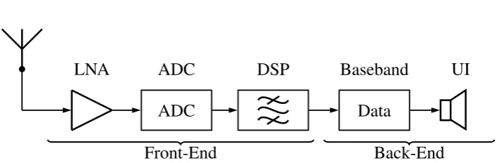
1.1.2 Design of the Full-Spectrum Receiver
The SHR is currently the most used radio receiver for RF-reception. It is a receiver with excellent reception characteristics, but it limits the received signals to certain Carrier Frequency (fc) by its mixers and the bandwidth
because of analog filters. On top of that the SHR makes use of an Intermediate Frequency (IF) stage, increasing the system complexity. In the FSR we want to capture all signals from DC up to fs
2 without pre-conditioning the bandwidth orfcof the signal before it is digitized.
BPF1 LNA BPF2 Mixer1 BPF3 VGA D Baseband
∼ LPF ADC S Data
[image:16.595.142.494.400.493.2]∼ P
Figure 1.1: Super-heterodyne receiver according to [1].
In figure 1.1 we present the architecture of the SHR. The first Band-Pass Filter (BPF) performs the pre-selection of the signal to reject images that are far away in the frequency band. BPF2 then performs another image-rejection after the amplification by the Low-Noise Amplifier (LNA). The first mixer (⊗) performs the frequency shift from RF to some IF to have BPF3 filter out the desired channel. The Variable-Gain Amplifier (VGA) performs an amplification so that the signal matches the full scale of the ADCs. The second mixer performs a translation from IF to baseband, after that the signal passes an Low-Pass Filter (LPF) and is finally digitized by the ADCs.
LNA
ADC
DSP
Baseband
UI
ADC
Data
[image:17.595.95.451.111.227.2]Front-End
Back-End
Figure 1.2: Full-spectrum receiver.
digital domain where they can be adjusted as desired. The mixing in the SHR is performed to shift the desired signal to the passband of the filters. Because we remove the filters in the FSR, mixing between stages becomes obsolete and we can remove them as well. The frequency translation to baseband remains necessary, but this can be performed in the digital part. Because the amplification of the VGA and the LNA is limited by the highest interferer, we have to determine its power. Then we can merge them to perform a fixed amplification and end up with the receiver architecture of figure 1.2.
1.1.3 Uses for Full-Spectrum Receivers
FSR technology is already successfully implemented in chips for DVB-receivers by NXP, Max Linear and Broadcom [13] [14] to replace the expensive tuners that are conventionally employed in those systems. When comparing the num-ber of components in figures 1.1 and 1.2 we can clearly see that the FSR has much less (analog) blocks than the SHR. The reduced number of components makes the FSR circuitry cheaper, creating budget for a better ADC.
The DVB-FSRs are employed in home entertainment systems and receive digital television and radio on several channels at the same time, limited only by the number of filtering paths and demodulators. We found that this ap-plication is possible because in wired systems the signal strengths are kept quite similar. This means the ADC does not have to cover such a wide range of strengths which relaxes the requirements on the design of the ADC. In wireless RF-communication the antenna is the first part of the receiver that introduces a certain bandwidth, making its design crucial for receivers. Mul-tichannel antennas are developed [15] as a (partial) solution to counter this property.
High-end FSRs could be interesting for intelligence agencies to monitor the
due to the sample frequency) and the number of demodulators for the different channels and transmission schemes (FM, QAM, PSK, etc.). Lastly the FSR lends itself perfectly for wideband communications because they are designed to receive a large bandwidth.
The FSR seems a very promising receiver architecture and very worthwhile to look into but there will be some considerations and trade-offs involved. The main challenge in its development will be for the ADC to receive both strong and weak signals at the same time.
[image:18.595.175.467.328.532.2]1.2
Problem definition
Figure 1.3: Implementation of a conventional 8-channel receiver.
1.2.1 Requirements
In this section we present the requirements for the signals that we want to receive with our FSR; this defines the specifications of our system. From [16] we find that the typical maximum signal strength for signals in the ether is defined as −13 [dBm]. Taking into account a small margin for this value we define the maximum input power 3 [dB] higher: Pin,max = −10 [dBm]. The smallest signal that can be received, defines the sensitivity of the receiver.
WiFimin WiFimax Bluetooth GPS FM
Sensitivity [dBm] -90 -65 -70 -130 -100
Maximum input signal [dBm]
-30 -30 -10 -90 (?) -13
Dynamic Range [dB] 60 35 60 40 87
Table 1.1: Table showing the minimum, maximum and range of signal strengths for various standards.
In table 1.1 the signal strengths are given for WiFi (802.11a/b/g/n) mini-mum and maximini-mum data rates [17], Classic Bluetooth [18], Global Positioning System (GPS) [19] and FM [20]. WiFi signals use a 22 [MHz] band, Bluetooth 1 [MHz], GPS 2 [MHz] and FM-radio ∼200 [kHz].
We choose to design an FM receiver as its modulation and demodulation is easily performed with the available tools. While FM can contain multiple signals for stereo and Radio Data System (RDS), we focus on a receiver for mono-audio as it is sufficient for our tests. A sensitivity of at least −90 [dBm] is a little higher than conventional FM receivers but it will allow us to re-ceive commercial radio signals not too far from the broadcasting tower. The strongest signal that can be expected is−10 [dBm] and the ADC will have to facilitate for this signal power as well.
An LNA is commonly used in receivers to increase the sensitivity. Ampli-fication only works if the signal power does not exceed the maximum input of the ADC. In conventional receivers interferers are filtered out early in the re-ceiver chain by BPFs. With a VGA the Dynamic Range (DR) of the rere-ceiver can be increased, because the desired signal may be amplified according to its strength. If no filtering is applied, like in the FSR, the maximum possible amplification depends on the strongest signal, which might be an interferer. With the maximum signal power that the FSR should handle we defined its full-scale of the. With it, we can use an LNA to provide a constant amplifica-tion.
LNAs typically amplify between 15 and 25 [dB] with a Noise Figure (NF)1 under 4 [dB]. The LNA will behave as a BPF because they can not uniformly amplify all frequencies . Typical values for our application range vary from
100 [kHz] up to 2[GHz] but other bands are possible. Because there is a lot of well designed LNAs suitable for use in FSRs, we expect its bandwidth not to be an issue. The amplification and noise-figure however, will have a definite impact on the performance of the receiver. We defined that the FSR receiver should detect signals at −90 [dBm]. With the LNA amplification of 20 [dB] and an NF of 4 [dB], the receiver can detect signals as low as −90 + 20 + 4 =−66 [dBm]. The strongest signal will be 10 [dBm] at the input of the ADC resulting in a DR of 76 [dB].
Because we are designing an FSR, we should be able to receive at least two channels as a proof of concept. Our ADC has an fs between 200 [MHz]
and 5 [GHz] so we can capture signals up to 2.5 [GHz] which covers the IEEE-802.11b WiFi band (2.4 [GHz]).
Because of the bandwidth of to the LNA we will be limited to the band from 100 [kHz] to 1000 [MHz]. The flatness and roll-off of the LNA will define whether its possible to take afc outside this band.
1.2.2 Feasibility
Amplitude
Potential Gain
S
1
S
2
P
in
,
max
P
in
,
min
DynamicRange
FS
SHR filter
Frequency
Figure 1.4: Dynamic range of two signals.
be-cause it is limited by the quantization step, we can calculate it when we know the number of bits (N) with equation 1.1.
DR = 20log10 2N (1.1)
If we want to receive S2 the ADC can sample the analog signal and it can be processed digitally. Signal S1 is represented by the LSB of the ADC, a single bit, which makes it very sensitive to errors caused by noise. On top of that the distortions caused by S2 can make it difficult to detect S1 as well.
In an SHR the analog filters are used to remove these strong interferers after reception. When S2 is filtered out, S1 can be amplified to match the full-scale of the ADC for the best reception. In the FSR there is no filtering before the ADC. This means that every signal, weak and strong, will appear at its input. Therefore it is important to determine how the FSR can deal with the reception of weak and strong signals at the same time.
On top of strong signals posing a challenge for the reception of small signals, Inter-Modulation Distortions (IMDs) caused by the harmonics can introduce problems as well. Due to nonlinearities of the LNA and the ADC, harmonics of these signals may be introduced and appear near or on top of the (small) signal of interest, causing distortions in the reception.
The bandwidth of each part in the receiver chain will put constraints and limitations on our receiver. The antenna, the LNA [21] and the ADC (mainly the Sample-and-Hold (S/H) circuit [22]) will each have a defined transfer func-tion which influences the signal. Each of the individual parts introduces some noise which can be combined for the whole receiver chain in the total NF of the receiver. The characteristics of the components that we use to build the system, require attention when determining the feasibility of an FSR that fulfills our requirements.
The digital signal processing that needs to be performed is not trivial because billions of samples per second will be produced by the ADC. The FPGA possibilities may be used to its maximum and special design tricks could be necessary to implement the hardware that can handle this kind of high data-rates.
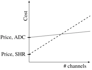
1.2.3 Costs
reception with multiple antennas to prevent the exclusion of channels. There-fore we leave out the antenna from the equation for the cost function. Both systems require a demodulator, so we leave it out of the equation as well. For an FSR system we require one amplifier, a good ADC and a DSP. When we want to make an SHR, we require 4 analog filters, two amplifiers, at least one mixer and an ADC.
For receiving additional channels with SHRs, we need a complete receiver per additional channel. This means that for each added channel, the cost per channel is increased by the cost of a single receiver. In the FSR implementation we require a second digital signal path, but no new ADC or other hardware is required, this gives it a much lower increase in cost.
We expect the traditional SHR to be a lot cheaper than the FSR imple-mentation due to a lower graded ADC, which gives it an initial advantage. For each additional channel we expect that for the FSR the increase in hardware cost is lower for than for an SHR, as we show in figure 1.5. So there will be an break-even point after which it will be cheaper to use an FSR instead of an SHR with a certain amount of receiving channels.
Cost
# channels Price, ADC
[image:22.595.231.414.369.507.2]Price, SHR
Figure 1.5: Cost functions of the FSR and the SHR.
1.2.4 Trade-offs
For ADCs there are typically 3 degrees of freedom: power, bandwidth and res-olution, from which a number of possibilities and limitations can be derived. In this section we cover the trade-offs we can make between these parame-ters. We also present two alternative implementations that make an efficient exchange between these parameters using specific signal processing effects.
Figure of Merit
scientists to compare ADCs. It also provides developers to make a rough estimation of the trade-off involved in ADC-design.
In [23] a classification is made to distinguish between different FOMs. They vary in the parameters they cover but almost all include the DR in some way. Usually the Signal-to-Noise and Distortion Ratio (SNDR) (equation 1.2) is used. This expresses the performance of the ADC in a relation between the maximum input (Pin,max) and the degradation caused by (quantization) noise (PNoise) and nonlinearities of the system (PDistortion).
SNDR = Pin,max PNoise+ PDistortion
(1.2)
FOMWaldenstates a one-to-one relation between resolution, expressed with the SNDR, and bandwidth: +1 bit ∝ 2×fs; this holds well for low-speed
ADCs (≤100 [MHz]) up to gigahertz converters. FOMThermal states that that bandwidth and resolution may be exchanged at a higher cost where each +1 bit ∝ 4×fs. This results in an exponential increase of the power if either is
increased; this holds for high-speed ADCs (≥1 [GHz]).
FOMWalden= GA1= SNDRdB+ 20×log10( fs
P) (1.3)
FOMThermal = GB2 = SNDRdB+ 10×log10( fs
P) (1.4)
However, from [24] we observe that for the high-frequency (flash) ADCs the power dissipation increases tenfold for each additional bit. The FOMs presented in [23] appraise resolution accordingly to make a proper estimation of the trade-offs involved for an FSR implementation. Therefore we can not use these FOMs as they are a tool for ADC designers. Instead we have to consider the direct comparison between the DR and the fs as a measure to
define the performance of ADCs.
In figure 1.6 we present the relation between the resolution and the band-width of different ADCs presented at the International Solid-State Circuit Conference (ISSCC) and at theVLSI and Embedded Systems Conference˝[2]. For low speed ADCs we can see the 30 [dB] degradation of the SNDR per decade of bandwidth is correct according to FOMW alden, but this does not
hold for high speed ADCs where−70 [dB / decade] is a more suitable approx-imation.
Bandpass Sampling Receiver
Sample Frequency (Hz)
SNDR (dB)
Figure 1.6: ADC survey of SNDR vsfs from [2].
BPF LNA ADC D Baseband
∼
LPF S Data [image:24.595.135.499.127.328.2]P
Figure 1.7: Bandpass receiver according to [3]
(fs<fc), where an image of the signal is projected in the baseband. Aliasing
removes the need for a frequency shift so a mixer is not needed in this design. Out Of Band (OOB)-interferers will be filtered out by the BPF so the requirements of the ADC DR are relaxed to only handle signal strength varia-tions of the targeted signal. The challenge of this architecture is in the design of a good filter with a very sharp roll-off, which completely blocks any inter-ferers while allowing the signal of interest to pass.
Direct conversion receiver
BPF LNA I
∼ LPF ADC
Q
Figure 1.8: Direct conversion receiver according to [3]
The bandwidth of a direct conversion receiver is fixed due to its filters. The mixing stage may be implemented using a digital VCO which allows a wide reception range and good channel selection. Because of the analog filters the constraints on the ADC are relaxed. This architecture requires a very careful design to prevent a DC offset from the mixer to appear at the ADC.
1.3
Prototype Full-Spectrum Receiver
The components of our prototype are based around an ML605 FPGA development-board from Xilinx [25]. To its High Pin-Count (HPC)-connector, we connect an FMC125 daughterboard, developed by 4DSP, containing an 8-bit, 5 [GHz] ADC from e2v [26]. For the (wireless) reception of the signals, we have an LNA [21] available to amplify the RF signal before it is fed to the ADC. The signal from the ADC is processed in the FPGA and sent via an Ethernet cable to a Personal Computer (PC).
1.4
Research questions
Following our wish to implement an FSR we formulated the following research question:
Can a Full-Spectrum Receiver, which meets our requirements for a practical receiver, be implemented using the available hardware for the prototype?
If not then:
1. what can we do to get as close as possible to our requirements?
2. what can we do to limit the design effort such that building the prototype fits in the scope of a graduation project?
3. given the current technology trends, when will it become possible to build a full spectrum receiver that meets our requirements?
1.5
Contributions
The main contribution of this thesis is a clear presentation on the requirements and the trade-offs involved in designing an FSR. The implementation with the available components, gives valuable insight about the reception characteris-tics and allows verification of the theory. After evaluating the results we could present the implications of the implemented receiver architecture. We present solutions to improve the receiver performance for future research. By studying the trends of ADCs we make a prediction when the implementation of an FSR that meets our requirements can become a reality.
1.6
Report outline
Related Work
This chapter presents the work of other researchers working on receiver tech-nologies that are used by or closely related to Full-Spectrum Receivers (FSRs). First we cover the research on several conventional receiver architectures. The second part of this chapter covers work on digital signal processing techniques.
2.1
Receiver Architectures
BPF LNA I
∼ LPF ADC
Q
Figure 2.1: Direct Conversion Receiver topology from [3].
In this section we present two other receiver architectures which use ana-log circuits to overcome the issues that the FSR suffers from and work that is performed on FSRs. Other receivers sacrifice bandwidth to enable the con-current capturing of their signals. A comparison of the techniques is given in [1].
2.1.1 Direct Conversion Receivers
The Direct Conversion Receiver (DCR)1, figure 2.1, originates from the homo-dyne receiver topology [27]. The Radio Frequency (RF) signal is first filtered to remove Out Of Band (OOB) and especially High-Frequency (HF) signals that could alias back to baseband. Then it is mixed to baseband using an
oscillator running at Carrier Frequency (fc), so the Analog-to-Digital
Con-verter (ADC) may sample at a frequency much lower than fc (but at least
at twice the bandwidth). This receiver topology has the serious drawback of introducing a Direct Current (DC)-voltage drift, caused by mixing the input with the local oscillator. This can be a major issue for some radio standards as presented in [28]. Nevertheless DCRs are used more often in receivers, for example in mobile handsets, due to their low part-count and complexity compared to the Super-Heterodyne Receiver (SHR).
2.1.2 Bandpass Receivers
BPF LNA ADC D Baseband
∼ LPF S Data
[image:28.595.145.478.262.400.2]P
Figure 2.2: Bandpass receiver topology from [3].
The Band-Pass Receiver (BPR)2 (figure 2.2) makes a very efficient trade-off between bandwidth and sample frequency (fs)3 by using aliasing (caused
by subsampling). The BPR requires a filter with a very sharp frequency roll-off (high quality factor) to allow this phenomena to occur without destroying the received signal with aliases and OOB interferers. Aliasing is already described in the early days of digital signal processing [29]. Due to the technical diffi-culties of implementing the required filters it took a long time before practical subsampling (bandpass sampling) became a possibility [30] and was applied in systems [19].
Recent studies mostly focus on the reception of multiple bands using a sin-gle ADC [31] [32] [18]. The drawback of this application is that it requires dis-tinct RF-filters for each band combined with careful alias-frequency-planning. This means the minimum sample frequency [33] is not always achieved in such systems and overdimensioning the component capabilities is required.
2.1.3 Full-Spectrum Receivers
We are looking to employ an FSR for wireless communications. Chips and products that use an FSR-architecture already exist for wired systems.
Com-2
Also referred to as subsampling receivers.
3A lowerf
panies have successfully implemented FSRs in their products, replacing the expensive analog tuners [14] [13]. We found claims that Digital Video Broad-casting (DVB)-satellite FSRs already exist, but little information could be found and demonstrations are planned for later this year [34].
2.2
Multirate Digital Signal Processing
In this section we discuss the digital processing part that provides the demod-ulator with the baseband signal that it requires. Typically a Digital Down Converter (DDC) [10] is used to translate the digital signal from RF to base-band. It consists of two parts, a mixer and a low pass decimating filter as depicted in figure 2.3. These parts do not enforce a specific implementation, so there are multiple variants available for each.
yM I
Data ∼
yM Q
Figure 2.3: Architectural overview of the DDC.
2.2.1 Digital Down-Converter Mixing Stage
For the FSR the DDC is a critical component because it has to mix a sig-nal from RF, which is generally in the gigahertz domain, down to baseband, around DC. While the filter may perform down-sampling, the mixer may not, because it can destroy the information contained in the signal, so mixing will have to be performed at the same rate as the fs.
drawback of this multiplier-less implementation is the not parallelizable (se-quential) implementation of one step in the algorithm. This creates a bot-tleneck limited by the speed of the platform, rendering implementations for gigahertz sampling rates infeasible4.
In [5] 128 parallel multiplicators are implemented to handle GHz sampling rates and mix the signal to baseband using a LUT. With a highfs, to mix low
frequency signals to baseband, we require an big LUT. Therefore the main drawback of this implementation is the need for a large memory to cover all frequencies.
Another implementation to mix the signal to baseband is the COrdinate Rotation for DIgital Computers (CORDIC) algorithm which has been exten-sively developed [40]. The size of the core (in an FPGA) is similar to that of a multiplier [41]. The implementation is multiplier-less and calculates the rotation of the I and Q signals to perform the frequency translation (to base-band). The CORDIC core performs complex signal processing in a single core, compared to the four multiplicators which are required when processing a com-plex signal with a LUT implementation. This algorithm can be performed in parallel and does not require as large a LUT as an NCO with multiplier im-plementation requires, making CORDIC a well suited imim-plementation for use on FPGAs.
2.2.2 Digital Filter Design
The FSR requires all the filtering to be performed in the digital domain, which means that filters are relatively easy to design, but they can become too large for the FPGAs on which they should be implemented. The tra-ditional Cascaded Integrator-Comb (CIC)-filter can not be implemented in parallel and thus its throughput is limited by the platform speed. This ren-ders the use of this class of filters useless when implementing an FSR. A recent implementation [5] uses multiple (cascaded) Finite Impulse Response (FIR)-filtering stages, which can be put to work in parallel. The clever use of the platform specifications to perform half-band filtering with basic-components allows them to implement three DDCs in a single Virtex-6 FPGA5.
4
If the sample rate is reduced to a manageable speed with other techniques, this imple-mentation may still prove very useful.
Design Considerations
In this chapter we cover the implications and requirements for a Full-Spectrum Receiver (FSR) system. We start at the front of the receiver chain by defining the signal we want to receive with the antenna. After that we cover the effects of the parts up to the Analog-to-Digital Converter (ADC). Following that we cover the digital signal processing which is required to present the signal to the back-end (demodulator). With the mentioned considerations for the FSR we can draw conclusions on the applicability of such a system.
3.1
Reception Characteristics
In this section we present the calculations and properties of the signal and hardware up to and including the ADC. With these calculations we can define the expected performance of our hardware in a receiver. For reference purposes we express the requirements that we found for practical receiver parameters again from chapter 1.
3.1.1 Signal Specifications
Our goal is to design an FM-receiver for mono-audio radio signals. In figure 3.1 we see that the audio signal is a 15 [kHz] band. This signal will be frequency modulated with the maximum deviation ∆f = 75 [kHz] resulting in total bandwidth (B) of the modulated signal BFM= 150 [kHz]. This signal should have Signal-to-Noise Ratio (SNR)≥10 [dB], otherwise demodulation will not be possible [42]. The use of an initial amplification is considered to have a positive effect on the reception of Radio Frequency (RF) signals, therefore we will make use of an Low-Noise Amplifier (LNA).
We defined the following desired characteristics for a practical receiver:
• Maximum (blocker) signal strength: Pin,max=−10 [dBm]
• Minimum signal strength (sensitivity): Pin,min =−90 [dBm]
• Dynamic Range (DR): Pin,max−Pin,min= 80 [dB]
Po
wer
Frequency (KHz)
0 15 19 23 38 53 57
RDS Stereo
[image:32.595.136.508.84.289.2]Pilot Mono
Figure 3.1: FM-baseband spectrum, from [4].
3.1.2 Maximum Received Power
The signals that will be received are bounded by the strongest signal in the spectrum, these signals are therefore called blockers. Following the research presented in [16] we assume they have a maximum power of−10 [dBm]. Equa-tion 3.1 presents the relaEqua-tion between the voltage range of the ADC (Vp-p), the termination resistor (R) expressed in Ω and the maximum input power (Pin,max) expressed in dBm.
Pin,max= 10log10 Vp-p 2√2
2
×1000 R
!
[dBm] (3.1)
The LNA provides an amplification of ∼20 [dB], therefore the ADC will receive Pin,max,ADC=−10 + 20 = 10 [dBm]; with a 50 [Ω] termination resistor and rewriting equation 3.1 this results in a required Vin,max,ADC = 2 [Vp-p]. For a DR of 80 [dB] we require at leastlog2(108020) = 13.3 bits [43].
SNR = 6.02×n+ 1.76 [dB] (3.2) Our ADC has 8 bits and following equation 3.2 from [44], we find the best SNRADC = 49.9 [dB] [43]. The input voltage range of the ADC VADC,p−p =
500 [mVp-p]. With equation 3.1 we find the maximum input power of the ADC Pin,max,ADC=−2 [dBm].
3.1.3 Minimum Received Power
The smallest signal that we can detect is defined by the noise floor, which is a combination of the thermal noise (NT), quantization noise and distortions.
Thermal noise is caused by the motion of electrons in an electric system and causes−174 [dBm] per hertz at an antenna temperature of 293 [K]. Quantiza-tion noise is caused by the number of bits used for the representaQuantiza-tion of a sig-nal. Other distortions are caused by nonlinearities in the LNA and ADC and are calculated using the Inter-Modulation Distortion (IMD)-characteristics of the systems.
3.1.4 Thermal Noise
The FM signal band is 200 [kHz]1 wide. We use equation 3.3 where we fill in Boltzmann’s constant (kB = 1.3806488e−23 [J/K] [41]), the antenna noise temperature (T= 293 [K]) and the bandwidth (B) to find the thermal noise floor in this band NT =−101 [dBm].
NT = 10log10(kBTB×1000) [dBm] (3.3) The thermal noise is uniformly spread white noise in the received spectrum and therefore affects the input SNR. The SNR of a received signal has to be high enough for a demodulator to process the signal. The thermal noise floor puts a fundamental limit on the minimal noise power, this enforces a minimum power for the received signal. In our FSR we will not be limited by the thermal noise because the noise floor for 2 [GHz]2 lies at 10log
10(kB×293×2e9) = −80.82 [dBm] which is below the sensitivity of our ADC.
To calculate the minimum required signal power we need to define the receiver Noise Figure (NF). For cascaded stages we can calculate the total NF with Friis’ formula for noise, shown in equation 3.4. The total NF will never get lower than the NF of the first stage of the receiver, so a low NF is desired. This relation also indicates that the gain of the first component can be used to suppress˝ the NF of components further in the chain. Thus a high gain in the first step is beneficial for the reception because gains later in the chain are less effective.
FTotal = F1+F2−1 G1 +
F3−1
G1G2 +... (3.4)
NF = PFS+ NT,1Hz−SNR−10log10(B) (3.5)
All these values must be used in their linear representation (we generally use the logarithmic representations in dB). The NF and the gain of the LNA
1
Because the actual band for our signal is a bit over 150 [kHz], we can take 200 for the ease of calculations because it is a worse-case.
are given by the datasheet [21]. For the NF of the ADC we use the calculations from [45] in equation 3.5 where PFS = 2 [dBm]; NT,1Hz =−174 [dBm]; SNR = 45 [dB]; B = 2 [GHz]. We calculate the linear representations of the values we already know and obtain the following values:
• NFLNA= 3 [dB]→ F1 ≈2
• GainLN A≈23.5 [dB] → G1≈100×.
• NFADC= 33 [dB] →F2 ≈2000
With these values and equation 3.4 we find for our receiver that NFTotal≈ 10 [dB].
3.1.5 Quantization Noise
Quantization is an effect that occurs in the conversion from a continuous valued signal to a discrete-valued signal. This occurs in digital signals because they are represented by a finite number of bits. This transformation introduces some loss of the signal’s information, which can be seen in figure 3.2. We used 3 bits for the representation giving us 8 quantization levels to show the effect.
The maximum introduced error by an ADC is ±q2 ×Vmax, where q rep-resents the smallest representable value, q = 21N and N is the number of bits used. The Root Mean Square (RMS) value of this error is Vmax,error×√q12. The resulting SNR can be calculated using equation 3.6 and is usually generalized to equation 3.7 [44].
SNRquantization = 20×log20( Vin,RMS
Vnoise,RMS) [dB] = 10×log10( Pin
Pnoise) [dB] (3.6)
SNRquantization= 6.02×N+ 1.76[dB] (3.7) Our ADC uses 8 bits for the digital representation of the sampled signal and has a maximum input voltage swing (full-scale) of VFS = 500 [mVp-p] resulting in a quantization step between two quantization levels of 2.58[mV]≈
1.95 [mV]. The SNR of our ADC is equal to SNRquantization≈50 [dB] [46].
3.1.6 Inter-modulation Distortions
0
20
40
60
80
100
−
1
−
0
.
5
0
0
.
5
1
Time
Amplitude
[image:35.595.90.457.128.393.2]Continuous
Discrete
Error
Figure 3.2: Quantization noise caused by representing a continuous valued signal with a 3 bit valued signal.
Amplitude
2S1−S2
S1 S2
2S2−S1
2S1
S1+S2
2S2
IMD2 Results IMD3
Results Signals
Figure 3.3: Inter-modulation distortion of two sine waves.
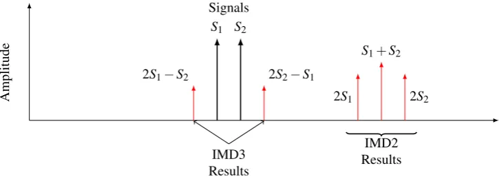
The IMDs are proportional to the carrier signal strength and therefore usually expressed in [dBc], this means they will become smaller with smaller signals.
[image:35.595.95.458.455.585.2]problem. The IMD3 distortions however, appear close to the original signals, as can be seen and this can cause distortion of the wanted signal3. Because they appear so close to the targeted signal it is hard to remove them with filtering which makes a low IMD very important for receivers.
In most conventional receiver techniques the IMD2 (and higher order even IMDs) appear far away from the original signal and are removed by analog filtering. Due to the large bandwidth of the FSR, even IMDs may appear close to other signals [48] and distort them. Meaning that a desired signal can be distorted by the IMD caused by other signals.
3.1.7 Spurious Free Dynamic Range
One way to express the IMD caused by a receiver is to express its Spurious-Free Dynamic-Range (SFDR). This defines a relation between the power of these IMD spurs relative to the signal power (fc) or the full-scale of the ADCs.
The SFDR of our ADC is given in the datasheet SFDRADC = 48 [dBc]. Mixers and amplifiers have a generalized model to determine the IMDs with so called intercept Point (IP) . The second and third order IP (IP2 and IP3) are used to calculate the performance. The input of the ADC will clip with too strong signals [49] and this makes the ADC too nonlinear to make use of this model. Therefore we have to review the effects of the separate components of our receiver chain.
With an expected maximum signal strengths of−2 [dBm] the spurs from IMD in the ADC are expected to have a maximum strength of PSpurs,max = Pin,max,ADC −SFDRADC = −50 [dBm] 3.4. Note that if no signals with −2 [dBm] are present at the input of the ADC, the spurs will be weaker but also the full-scale is used inefficiently. For Frequency Modulation (FM) we require SNRFM ≥ 10 [dB] which means that the weakest detectable FM signal will have to be−40 [dBm] at the input of the ADC, otherwise it may be distorted by IMDs.
With the IP3,LNA = 14 [dBm] we can calculate the IMD3 caused by the LNA. Using equation 3.8 from [48], where the (thermal) noise floor N0 = −81 [dBm] with a bandwidth B = 2 [GHz], we find SFDRLNA ≈64 [dB]. This means that the input power to the LNA will be limited by the ADC input range. Therefore we expect that the LNA to have little negative influence on the total SFDR of our system.
SFDRdBm= 2/3(IP3−N0) [dBm] (3.8)
3
Amplitude
Spur
Signal
FM
−
2 [dBm]
−
50 [dBm]
−
40 [dBm]
SFDR
=
48 [dB]
[image:37.595.99.456.131.376.2]SNR
FM
Figure 3.4: Maximum signal, spur and minimum FM signal strengths.
3.1.8 Summary
The characteristics of the ADC impose the dominant limitations on the re-ceived signal. Pmax,ADC pushes the maximum received power on the LNA to ≤ −22 [dBm]. On the lower side the thermal noise floor enforces a mini-mum power of −81 [dBm], but before that, the ADC reaches the soft-limiting bound PSpurs,max = −50 [dBm] caused by the SFDR and 2 [dB] lower the hard-limited bound caused by the quantization. Add to that a gain of 20 [dB] from the LNA, resulting in signal strengths that can be received by the LNA between −70 [dBm] and−22 [dBm] before nonlinearities occur and the signals are destroyed. For the demodulation of FM signals we require an SNR of at least 10 [dB], so the minimum power of the signal we receive should be −60 [dBm].
3.2
Digital Signal Processing
Following the traditional Digital Down Converter (DDC) architecture, shown in figure 2.3, we have to perform a frequency translation to baseband and filtering, not necessarily in that order. We have the option to perform the conversion to baseband using a mixer or by downsampling. For the filtering we can use low pass, high pass and bandpass filters; which may be cascaded to create a distinct frequency plan. Different filter implementations may be considered but we can already rule out the use of Cascaded Integrator-Comb (CIC)-filters [50] because they can not match the speed for the desired sam-pling rates. Infinite Impulse Response (IIR)-filters are also unusable in the FSR because of their internal feedback mechanism which limits the implemen-tation to the platform speed. The platform speed of our FPGA is≤600 [MHz] while sample frequency (fs) will be at least twice as high.
3.2.1 Frequency Translation Using Decimation
A high-speed RF-Finite Impulse Response (FIR) filter could be implemented to use downsampling (decimation) as a way to mix the signals to baseband with the aliasing effect. With Filter Design and Analysis-Tool (FDA-Tool) from Matlab we designed a suitable bandpass (equiripple) filter following [51]. We use the parameters below to obtain a passband of 200 [kHz], just enough for an FM signal and an Out Of Band (OOB) attenuation of 13 [dB].
• Fs: 1.25 [GHz]
• Fstop1: 100.05 [MHz]
• Fpass1: 100.1 [MHz]
• Fpass2: 100.3 [MHz]
• Fstop2: 100.05 [MHz]
• Astop1: 13 [dB]
• Apass: 1 [dB]
• Astop2: 13 [dB]
The resulting filter is shown in 3.5, which perfectly displays the size of the passband compared to the total bandwidth. This filter performs the filtering and frequency shift to baseband in a single step but requires 16663 multipli-cations per sample. Our FPGA contains 768 DSP-slices to multiplimultipli-cations, which means this filter design is infeasible for our sample rate.
0 100 200 300 400 500 600 −60
−50 −40 −30 −20 −10 0
Bandpass Equiripple
Ma
gn
it
u
tde
(dB)
[image:39.595.90.416.126.301.2]Normalized Frequency (rad/sample) Frequency (GHz)
Figure 3.5: High order filter providing a 200 [kHz] bandpass filter at fs =
1.25 [GHz] with 13 [dB] OOB attenuation.
Using cascaded filters allows the use of aliasing in combination with filter-ing, but signals that are not mixed to baseband require bandpass filters. This means that a low- and a high pass filter will be required, effectively doubling the amount of filter-taps (multiplications) required. Therefore it is undesirable to only use for the down-conversion of a signal.
3.2.2 Decimating FIR-filter Implementation
Ternary Adder
x1
x2 ×2 ×14
y2 y
x3
Figure 3.6: Extended version of half-band filter from [5].
[image:39.595.100.434.486.648.2]of this filter are the raw values from the ADC, 8-bit values for each sample. x2 must be multiplied by 2, to realize this, we shift in a ’0’ on the right of the vector increasing the vector to 9 bits.
0 0.1 0.2 0.3 0.4 0.5 0.6 0.7 0.8 0.9
−70 −60 −50 −40 −30 −20 −10 0 Ma gn it u tde (dB)
[image:40.595.141.500.197.369.2]Normalized Frequency (rad/sample)
Figure 3.7: 3-taps half-band filter transfer function created using FDA-Tool.
The inputs are added together with a ternary adder, registers may be used to pipeline the process but care must be taken that the number of registers remains the same for all parallel placed adders. The result will grow by 3 bits to N+3 because of the shift and addition. It must be divided by 4 to prevent unwanted gain, this can be performed in a fixed-point representation by shifting the point two places to the left. With the FDA-Tool we find the transfer function of this filter presented figure 3.7.
This filter is minimal in size, capable of running at a high speed, paralleliz-able and provides a−3 [dB] cut-off frequency at fs
4. All these properties make it an ideal first step for a cascaded filter structure, but only if the targeted signal is below the cut-off frequency.
3.2.3 Frequency Translation With Mixing
Applying a frequency down conversion of a signal is usually performed by multiplying the input signal with a complex Carrier Frequency (fc) to translate
it to baseband. In [5] a Look-Up Table (LUT) is used to store this complex sine wave for the carrier frequency. While actually only 1/4th of a sine wave is required to create a full sine-wave, the logic will have to work at the fs
of the ADC. The lowest fc will define the size of the LUT. To translate a
signal withfc= 200 [MHz] and fs= 5 [GHz] to baseband we require of a full
sine wave containing 2005e9e6 = 25 samples. With a platform clock frequency of 600 [MHz], at leastd 25
parallel to compute the multiplications for this implementation. In practice this amount will probably be higher because the maximum platform rate of 600 [MHz] may not be achieved.
The required memory has to be implemented for each multiplier, because each multiplier needs to access a different value of the sine-wave at the same time. The memory must contain 5e9−1 samples to be able to mix frequencies with a carrier frequency between Direct Current (DC) and fs
2 to baseband. If we can make number of values equal to (a multiple of) the number of multipliers (N); then we only need to store 1 in N values for each multiplier.
If we consider a more practical implementation the constraints on the processing may be further reduced. With a minimal fc of 400 [kHz] we only
require one in 10×5 [GHz]400 [kHz] = 1250 samples. To store the sine waves as 14-bit values (SNRQuantization ≈84.2 [dB]) we require 2500×14 = 17500 [kbit]
of storage. This fits in two 18 [kbit] Xilinx block-Random-Access Memorys (RAMs) [53] and with 9 multipliers we require 18 of these to store the values for the I and Q paths.
In similar research we found that using a COrdinate Rotation for DIgital Computers (CORDIC)-algorithm [54] can provide a viable solution in FPGAs. In [55] we find that the maximum achieved rate for a CORDIC implementation on our FPGA to be∼340 [MHz]. Considering a sampling frequency of 5 [GHz] we require 16 cores in parallel to perform the down-mixing of a signal to baseband. The CORDIC implementation works with an accuracy of up to 16 bits.
Both implementations scale linearly with the data-rate to a minimum of 1 core if digital signal processing is applied before mixing. The size of a complex multiplier is about the same size as a CORDIC-core. The memory required for the LUT is higher for the multiplier implementation but considering only practical applications this may not be a problem.
3.2.4 Summary
There are many techniques and tools available to provide the required digital filtering and frequency translation for the FSR. Multistage filtering is neces-sary to cope with the high data rates because performing the required filtering in a single-stage requires too much resources. With CORDIC-cores we can translate any arbitrary signal from our input to baseband while a LUT imple-mentation requires optimization steps that limit the flexibility. When the mix-ing is done before the down-samplmix-ing, followmix-ing the classic DDC-architecture, we can use Low-Pass Filters (LPFs) instead of Band-Pass Filters (BPFs).
can be made between the required resources of the FPGA and the capabilities.
3.3
Conclusions
Full-Spectrum Receiver
Design
In this chapter we present the receiver we implemented to test and verify our analytical results in practice. The main goal is to create a wireless FM-radio receiver for frequencies up to 2.5 [GHz] by connecting the provided Analog-to-Digital Converter (ADC) and Field-Programmable Gate Array (FPGA)-board to a Personal Computer (PC). First we give an overview of the used hardware and the test equipment. This provides insight of the system shows the limitations and bottlenecks. Then we discuss the choices we made and give an overview of the implications. The realization and verification steps of the system are presented to draw conclusions about our implementation compared to the Full-Spectrum Receiver (FSR)-design.
4.1
Receiver Hardware
LNA ADC FPGA
IN ADC OU T
[21] [56] [25]
Figure 4.1: Designed system hardware overview.
In this section we give an overview of the hardware that we used to im-plement and test our receiver. In figure 4.1 we show the receiver architecture that we use for our system. We also present the transmitter devices that we used to create a signal for our receiver.
4.1.1 LNA: ZFL-1000LN+
The LNA has an in- and output using SMA-connectors impedance matched at 50 [Ω] to both the antenna and the ADC. The maximum input power is 5 [dBm] which is well within the maximum received power strength we defined: −10 [dBm].
The directivity of>18 [dB], stated in the datasheet, is an indication of its linearity [57]. This is considered good enough to not have to worry about it in our system. The supported bandwidth is defined from 100 [kHz] to 1 [GHz]. The provided gain is typically 20±0.5 [dB] at Vsupply = 12 [V] with a Noise Figure (NF) of∼3 [dB].
[image:44.595.154.486.291.545.2]4.1.2 ADC-board: FMC125
Figure 4.2: FPGA Mezzanine Card, FMC125 [6].
The FMC125 [56] daughter board that is used in this research contains an EV8AQ160 ADC [26]; a picture can be seen in figure 4.2. Figure 4.3 provides a schematic overview of all the inputs (left side) and outputs + control (right side), as well as a rough sketch of the internals.
The board has four Sub-Miniature version C (SMC)-connectors for input signals, terminated with a 50 [Ω] resistance. Each of these channels contains an ADC that can sample at frequencies between 200 [MHz] and 1.25 [GHz]. When feeding the same signal to all four inputs, a combined sampling rate of fs = 5 [GHz] may be achieved. The input bandwidth per channel is defined
Figure 4.3: FMC125 block diagram from [6].
of 500, 600, 1500 or 2000 [MHz]. The maximum input voltage for each of these inputs is 500 [mVp-p] with an input resistance of Rin = 50 [Ω], with formula 4.1 we obtain the maximum input power Pin,max = −2 [dBm]. The board also provides an external clock and trigger (synchronization) interface, as well as an HDMI-port which can act as a transceiver, but these functions are not used in our design.
Pin,max= 10log10( V2
in,RMS Rin ×
1000) [dBm] (4.1)
The FPGA Mezzanine Card (FMC) interface is defined in the VITA 57˝ standard. The FMC125 is a High Pin-Count (HPC) FMC, which allows it to be connected to the ML605 FPGA development board using the HPC-interface, which supports up to 400 pins. We use this port as a Low-Voltage Differential Signal (LVDS)-interface, which provides up to 1 [Gb/s] throughput per pin pair. For the full interface the FMC125 requires 4 ports ×8 bit/Sam-ple×5 GSample/sec = 160 [G/sec]. This requires 4 ports×8 bit/Sample = 32
The FMC125 board is controlled via an I2C-bus which is incorporated in the HPC connector. This connection allows interfacing with the periph-erals on the FMC125-board. The I2C bus allows direct access to the Elec-trically Erasable Programmable ROM (EEPROM) [58] and the temperature sensor [59]. An I2C-Serial Peripheral Interface (SPI)-bridge [60] is used to access the registers of the clock-generator chip [61] and the ADC for configu-ration and calibconfigu-ration purposes.
4.1.3 FPGA: ML605
We will use an ML605 [62] development board which contains a Virtex-6 FPGA1. The use of an FPGA in an FSR provides the required processing power and is highly reconfigurable logic which enables the reception of signals at different frequency bands.
The FMC-daughter board connects to the HPC-connector of the FPGA-board. The HPC-connector includes an I2C interface for a 2-way communica-tion with the daughterboard.
The ML605 uses the 10/100/1000 Tri-Speed Ethernet interface to send the data to the PC. This connection is used to control the FPGA program and send data to the PC.
The FPGA uses the LVDS pins to receive the data from the ADC. These pins each provide a maximum data rate of 1 [Gb/s], which means it can only transfer the data from the ADC-board when it is multiplexed; the data rate is 625 [Mb/s] per input. The FMC specifications require that the clock must be included in the interface. Therefore, all four channels (with multiplexed data) have their own clock signal.
The reference design for the FPGA uses 10/100 [Mbit] Ethernet. With a limited time available for the design, we decided we did not need to use the gigabit Ethernet connection. Together with the minimum sampling rate this puts bounds on the required data-rate reduction in the FPGA.
Because the ADC produces samples at a rate of 1.25 [GS/s] and Ethernet only handles 100 [Mb/s]≈12 [MB/s], this requires a data reduction factor of at least 110.25ee69 = 125.
4.2
Test Equipment
In this section we introduce the hardware that we used to test our receiver. To create the signals we use GNU-Radio Companion (GRC) on a PC connected to an Universal Software Radio Peripheral (USRP), with a Low-Frequency Transmit (LFTX) daughterboard, to create the analog signals. These signals are then sent to our Vector Signal Generator (VSG) to be mixed to the desired frequency.
4.2.1 Universal Software Radio Peripheral
To transform the digital signal, generated by a PC, to the analog domain we use an USRP [63]. The USRP connects via Universal Serial Bus (USB) to the PC so the data rate is limited to 8 [MS/s]. For an Frequency Modulation (FM) signal with a deviation of 75 [kHz] we have a total (complex) bandwidth of 150 [kHz]. Because of Nyquist we require to sample at least at twice the highest frequency, requiring a sample rate of over 300 [kHz]. This is well below the maximum sample-rate of the USB connection.
An LFTX daughterboard is connected to the USRP which we use to cre-ate an analog complex signal (I/Q-pair). The LFTX-specifications stcre-ate that its bandwidth is 33 [MHz], but we will only be using the baseband signal generated with the PC which is not more than the bandwidth of the USB port.
4.2.2 Vector Signal Generator
To translate our signals to the desired Radio Frequency (RF) we use the SMBV100A VSG [64]. It allows us to put our signals on a Carrier Frequency (fc) between 9 [kHz] and 6 [GHz] with a signal strength between−145 [dBm]
and +18 [dBm]. The maximum bandwidth of the provided I/Q signal may be 500 [MHz], which is well above the width of our test signal.
4.3
Trade-Offs
In this section we describe the trade-offs we had to make due to the limitations imposed on our system by hardware and time. Normally decimation is used for the data rate reduction, but for our project we found that implementing digital filtering in the FPGA was impossible. Therefore we implemented down-sampling without filtering, which causes signal aliasing. We cover the main problems of this phenomena and show how we use it in our design.
4.3.1 Aliasing Explained
Aliasing appears with all digital signals and is caused by the discrete repre-sentation. It results in the frequency spectrum repeating every multiple of sample frequency (fs). The effect can be observed in figure 4.4 where some
aliases of the signal are indicated but actually it goes on infinitely. Usually digital signal processing is only performed in the baseband (= 1st Nyquist-zone) and aliasing is not considered a problem. But when signals from outside the baseband are also sampled, the aliases can interfere with each other (at baseband) when they overlap.
trade-offs to be made when sub- or down-sampling. Too little subsampling means inefficient use of the available resources, so maximum subsampling is desired. However, using the aliases of signals when sub- or down-sampling has its limits because of the minimum required bandwidth.
Amplitude
0 fs
2 fs 32fs 2fs
−fs
2
Signal Baseband Alias
Aliases Baseband
Frequency Nyquist-Zone 1
[image:48.595.142.502.199.292.2]Zone 2 Zone 3 Zone 4 Zone 5
Figure 4.4: Aliases of a baseband signal
4.3.2 Folding
We show what happens if two frequency bands are received by the system but fold over each other. Take two signal bands in the spectrum as in fig-ure 4.5(a). What is clear is that the baseband aliases are separated. Now when we take two arbitrary signals like in figure 4.5(b) it can go wrong. Here the baseband aliases of both signals fold on top of each other, rendering them both useless [32].
Amplitude
Signals
0 fs
2 fs 32fs 2fs
Baseband
Frequency
(a) Correct signal folding.
Amplitude 0 fs
2 fs 32fs 2fs
Signals Aliases
Frequency
[image:48.595.158.484.488.669.2](b) Aliases folding on top of each other.
4.3.3 Nyquist Bandwidth
Too much subsampling will result in the Nyquist band being violated, which is very bad. This effect is demonstrated by adjusting the scale on the frequency axis accordingly. The signal in 4.6(a) is the signal with an appropriate sam-pling frequency showing its alias in the baseband. In 4.6(b) we applied too much subsampling, violating the Nyquist-bandwidth. As observed, the signal aliases interferes with the baseband signal (or alias), resulting in the loss of information.
Amplitude 0 fs
2 fs 32fs 2fs 52fs 3fs Frequency
(a) Correct amount of subsampling.
Amplitude 0 fs 2fs 3fs 4fs 5fs 6fs 7fs 8fs Frequency
Distortion
[image:49.595.114.440.260.439.2](b) Too much subsampling causing signal distortion at baseband.
4.3.4 Noise Folding
Theory [30] describes that just like every signal, noise will fold to baseband if it is not removed by filtering. The expected Signal-to-Noise Ratio (SNR)-degradation is described by equation 4.2. This phenomena is graphically pre-sented in figure 4.72. In this picture, f
s would be around 400 [kHz], which is
two times more than our maximum FM signal (180 [kHz]).
Amplitude
0 fs
[image:50.595.138.504.290.386.2]2 fs 2fs 3fs 4fs Frequency5fs
Figure 4.7: Graphic illustration of noise folding to baseband [7].
DSNR= 10log10(n) [dB] (4.2)
This is 3125×smaller than the input bandwidth of 2 [GHz]. According to 4.2 this should result in a SNR degradation of 10log10(3125) ≈ 35 [dB] due to down-sampling. However, the signal power is unaffected by filtering so it may pass through the subsampling-block without being attenuated, meaning the signal-power remains the same. With no filtering, it can not be that To be able to do that, we first distinguish the different sources of noise in our receiver:
• RF-noise in the signal before the signal enters the ADC caused by atmo-spheric and environmental effects, the design has no influence on this.
• Clock jitter of both the Sample-and-Hold (S/H) circuit and the sampler causing respectively aperture jitter and sampling clock jitter.
• Thermal noise caused by the physical properties of electrons.
• Quantization noise caused by the discretization of a continuous valued signal.
2
Quantization Noise
We can assume that quantization noise is uniformly distributed in the spec-trum [44]. Quantization will not reduce the SNR when subsampling, because the quantization noise of a 1 [Hz] sampler has the same SNR as a 1 [GHz] ADC. The quantization error is directly linked to the resolution of the ADC: 20log10(2N) = 48 [dB]. Following the fact that he ADC can receive a maxi-mum signal strength of −2 [dBm], any signal under −50 [dBm] at the input of the ADC will be lost due to its quantization noise.
Aperture and Clock Jitter
An ideal clock-circuit would produce a perfect pulse or square wave but phys-ical constraints prevent that. The effect is observed in figure 4.8 where a variation in the sample time (∆t) results in a variable sample value(∆s(t)). The variation in the clock is called the clock jitter and the effect it causes is
Time
Amplitude
τ
∆s(t)
[image:51.595.90.460.350.434.2]∆t
Figure 4.8: Clock and aperture jitter [8].
referred to as phase noise. The Signal to Jitter Noise Ratio (SJNR) is depen-dent on the maximum clock-jitter (tcj) and the maximum frequency (fmax) SJNR = 20log2π∗t 1
cj×fmax; where tj is the maximum clock jitter andfmax the
maximum input frequency.
tj =
q
(tcj)2+ (taj)2 (4.3)
According to [65]:Since the aperture-time variations are random, these volt-age errors behave like a random noise source˝; thus the SJNR is the maximum random white noise that’s generated by clock jitter. In [66] we find that the total jitter tj is the combination of the clock jitter (tcj) caused by the
clock-ing circuit and the aperture jitter in the ADC(taj), equation 4.3. Aperture
jitter is the variation (uncertainty) in time between two samples, expressed as τ in figure 4.8. In the data sheet of the ADC [26] we find the following values: taj ≤300 [fs] and tcj ≤500 [fs] resulting in a totaltj ≤583 [fs]. With
maximum value at the cutoff-frequency, where the signal is already attenuated by 3 [dB].
Thermal Noise
Thermal noise is noise caused by the motion of electrons in the system. The total thermal noise power (NT) is calculated by using the input impedance of a system using equation 4.4. Boltzman’s constant kB = 1.380,648,8× 10−23 [J/K], the normalized antenna temperature (T) is generally taken at T = 293 [K] and our the bandwidth B = 2 [GHz]. This results in a NT = −81 [dBm].
NT= 10log10(kBTB×1000) (4.4)
4.4
Expectations
In this section we combine the theory from chapter 3 with the trade-offs to get a complete overview of effects and limitations of the system that we created. To present the complete system there are considerations concerning the signal power levels in the different stages. First we regard the individual parts of the receiver to quantify the minimum and maximum signal strengths. We also discuss the required signal power from the sending side by regarding the losses caused by the air-transmission and the performance of the receiver system.
4.4.1 Signal Strength Expectations
The minimum signal strength that can be received by any receiver is defined by its thermal noise floor. For our receiver this is set by the input bandwidth of the ADC (2 [GHz]) which results in a thermal noise floor at the antenna of −81 [dBm]. This thermal noise is increased by the noise-factor (NF) of the receiver. For cascaded components the total noise-factor (NFT) of a receiver is calculated with equation 3.4 where we use the linear numerical-magnitude representation of the gain (G) and NF (F). The NF of the Low-Noise Amplifier (LNA) is specified in the data sheet; the NF of the ADC is calculated using 3.5. Our receiver has a total noise-factor NFT ≈10 [dB].
Pmax Pmin Gain G NF F
TX 20 [dBm] 0 [dBm] - -
-Antenna - - 6 [dBi] - -174 [dBmHz ]
Attenuator 27 [dBm] 0 [dBm] -30 [dB] 10−3s
-LNA 5 [dBm] -82 [dBm] 25 [dB] 316 4 [dB] 2.5
[image:52.595.136.503.609.698.2]ADC -2 [dBm] -50 [dBm] 0 [dB] 1 34 [dB] 240
![Figure 1.1: Super-heterodyne receiver according to [1].](https://thumb-us.123doks.com/thumbv2/123dok_us/9889328.490171/16.595.142.494.400.493/figure-super-heterodyne-receiver-according-to.webp)
![Figure 1.7: Bandpass receiver according to [3]](https://thumb-us.123doks.com/thumbv2/123dok_us/9889328.490171/24.595.135.499.127.328/figure-bandpass-receiver-according-to.webp)
![Figure 2.2: Bandpass receiver topology from [3].](https://thumb-us.123doks.com/thumbv2/123dok_us/9889328.490171/28.595.145.478.262.400/figure-bandpass-receiver-topology-from.webp)
![Figure 3.1: FM-baseband spectrum, from [4].](https://thumb-us.123doks.com/thumbv2/123dok_us/9889328.490171/32.595.136.508.84.289/figure-fm-baseband-spectrum-from.webp)

![Figure 3.5: High order filter providing a 200 [kHz] bandpass filter at fs =1.25 [GHz] with 13 [dB] OOB attenuation.](https://thumb-us.123doks.com/thumbv2/123dok_us/9889328.490171/39.595.100.434.486.648/figure-high-order-lter-providing-bandpass-lter-attenuation.webp)
