RESEARCH ARTICLE
DESIGN OF ENERGY EFFICIENT RANDOM ACCESS MEMORY CIRCUIT USING STUB SERIES
TERMINATED LOGIC I/O STANDARD ON 28NM FPGA
Alok Kumar, Gaurav Kumar Sharma, Anjan Kumar, *Tarun Agrawal and
Vivek Srivastava
Department of Electronics and Communication Engineering, G.L.A. University Mathura, U.P. India
ARTICLE INFO
ABSTRACT
This paper is based on the designing of energy efficient memory circuit using various IO standard of SSTL logic family on 28nm (Artix-7) Field Programmable Gate Array (FPGA). We are using Xilinx ISE simulator version 14.2, Verilog hardware description language and Artix-7 FPGA. Six different SSTL IO standard are compared with each other to find the most power efficient among them. The design has been tested for power consumption at different operating frequencies as of Intel processor that are at Intel I-3 5005U 2.0 GHz, Intel I-3 5015U 2.1. GHz, Intel I-3 5157U 2.5 GHz, Intel I-5 3380M 2.9 GHz, Intel I-5. 3340U 3.1 GHz and Intel I-7 3370K 3.5 GHz to check the compatibility of the design with processors available in the market and to find most efficient IO standard at different operating frequencies and at two different temperatures i.e. 25°C and 50°C.
Copyright © 2015Alok Kumar et al. This is an open access article distributed under the Creative Commons Attribution License, which permits unrestricted use,
distribution, and reproduction in any medium, provided the original work is properly cited.
INTRODUCTION
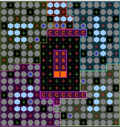
RAM stands for Random Access Memory, it is now an integral part of the electronic systems (1). It is fast memory with volatile in nature (5). It makes the access of data and system faster. There are two kinds of RAM, Static RAM and Dynamic RAM. There are various IO standard families present with different feature sizes (channel size of transistor) and therefore the selection of correct family among the various different families is very important to design most power efficient digital circuit (8). In this paper, we are using SSTL IO standard logic family. Stub Series Terminated Logic is an input/output standard which is used to match the impedance of the line, port and device of the device being undertaken (6). Therefore, selection of most efficient SSTL logic family among different available class of SSTL logic family plays a very important role for making energy efficient design (10). This paper is based on the implementation of RAM on XC7A100T device from Artix-7 FPGA family having feature size of 28nm (7) and -2 speed grades. Artix-7 XC7A100T device has 101440 logic cells, 4860 kb block RAM, 240 DSP slices and 300 IO pins. For designing energy efficient RAM, we have used SSTL IO standard. In this paper we are using six different IO standard as shown in Figure 1, they are SSTL 135,
*Corresponding author: Tarun Agrawal
Department of Electronics and Communication Engineering, G.L.A. University Mathura, U.P. India
SSTL 135_R, SSTL 15, SSTL 15_R, SSTL 18_1 and SSTL 18_II. Each SSTL IO standard that we have used to design the RAM is analyzed for power consumption at 2 GHz, 2.1 GHz, 2.5 GHz, 2.9 GHz, 3.1 GHz and 3.5 GHz operating frequency. This approach will help us to find the most power efficient SSTL IO standard and its compatibility with Intel I series processors.
The six different processors whose operating frequency we are using are Intel I-3 5005U 2.0 GHz, Intel I-3 5015U 2.1 GHz, Intel I-3 5157U 2.5 GHz, Intel I-5 3380M 2.9 GHz, Intel I-5 3340U 3.1 GHz and Intel I-7 3370K 3.5 GHz. SSTL IO standard can avoid the transmission line reflection by matching the impedance of transmission line, device, input port and output port.
SSTL IO standard has already been used for power efficient
design of various digital circuits like image ALU (Kumar et
al., 2013), parallel integrator (Das et al., 2014), VCM (2013),
ROM (2014), clock gated RAM (2013). The power dissipation in the RAM can be divided into two parts, static power and dynamic power. Dynamic power is the sum of clock, signal and input/output power. Total power dissipation is the sum of dynamic power and leakage power. In section IV power analysis is done for a constant frequency and different SSTL IO standard.
ISSN: 0976-3376
Vol. 06, Issue 08, pp. 1699-1706, August, 2015Asian Journal of Science and TechnologySCIENCE AND TECHNOLOGY
Article History:
Received 20th May, 2015
Received in revised form
29th June, 2015
Accepted 30th July, 2015
Published online 31st August, 2015
Key words:
Literature review
For designing of Digital system there are two hardware description languages, VHDL and Verilog. In this work Verilog language is used as a Hardware Description Language on Artix- 7 FPGA. There are 6 different SSTL taken in order to search for the most energy efficient IO standard for low power design. To get circuit with better performance in terms of low cost, high
speed and power efficient circuit it is important to choose the I/O standard for most efficient designing. when image ALU operates at frequency 1THz device with I/O standard
SSTL18_I_DCI, Family Virtex-6 FPGA, there is 45.55% decrease in IO power and 20.50% in Clock power as compared to SSTL18_II IO Standard (1). The increase in Signal Power and Logic Power is relatively small in magnitude than decrease in clock power that translates to decrease in overall dynamic power (5). The clock power consumption of Clock Gated 65536x16-bit dual-port Random Access Memory is 38.89% (on 1GHz frequency) and 41.3% (on 10GHz frequency) lesser than the clock power consumption of 65536x16-bit dual-port RAM without using clock gating Techniques (5). When ROM is operating with frequency of latest INTEL-i7 processor to test the compatibility of design with the latest hardware in use. When there is no any demand of peak performance, then power can be save 75% signal power, 74.5% clock power, and 30.83% I/O power by operating our device with 1GHz frequency in place of 4GHz Frequency. When there is no change in dynamic power parameter that is signal power and clock power but SSTL2_II_DCI having 80.24%, 83.38%, 62.92%, and 76.52% and 83.03% more I/O power
consumption with respect to SSTL2_I, SST18_I,
SSTL2_I_DCI, SSTL2_II, and SSTL15 respectively at 3.3GHz (4).
Block diagram of memory
In this work, we are using a Random Access Memory (RAM) circuit which has 6-bit address bus and 64-bit data input and output bus with Stub Series terminated Logic Input/output standard with size of 28nm FPGA to enhance the power consumption and to make circuit more power efficient circuit.
A. RTL Schematic of the Memory
Figure 1 shows the RTL schematic of the circuit. R
Figure 1. Different types of I/O standards
TL stands for Register Transfer Level. It is used in hardware description languages like VHDL and Verilog to create high-level representation of circuit and it also shows the implementation logic of the digital circuit that how data flows in and out from the circuit.
Figure 2. RTL Schematic of Memory Chip
B. Top Level View of Memory Package Pins
Figure 3 shows the top level view of memory package pins of the memory. It includes total 324 pins out of which there are 238 are IO bank pins and 86 backless pins. The design also has total 137 ports out of which there 6 address ports, 64 data input 64 data output ports and 3 scalar ports one for each enable, clock and write enable.
Figure 3. Memory Package Pins implemented using Verilog HDL
Power analysis of the memory circuit
The aim of the design is to reduce power consumptionand make
Figure 4. Categorization of Power
A. Power Dissipation with SSTL 135 I/O Standard
This section is based on the analysis of power consumption by SSTL 135 I/O standard at six different operating frequencies i.e. 2.0 GHz, 2.1 GHz, 2.5GHz, 2.9 GHz, 3.1 GHz and 3.5 GHz as of Intel I-series processors as mentioned in section I. Table 1 shows static and dynamic power consumption of SSTL standard at different operating frequencies.
Table 1. Power Consumption of SSTL 135 I/O standard
Freq. Temp CLK Signal BRAMs IOs Leakage Total
2.0 GHz
25°C 0.01 0.026 0.114 0.483 0.044 0.677
50°C 0.01 0.021 0.05 0.389 0.078 0.547
2.1 GHz
25°C 0.01 0.027 0.12 0.494 0.044 0.696
50°C 0.01 0.022 0.053 0.395 0.078 0.588
2.5 GHz
25°C 0.012 0.032 0.143 0.539 0.044 0.72
50°C 0.012 0.026 0.063 0.421 0.078 0.6
2.9 GHz
25°C 0.014 0.038 0.166 0.584 0.044 0.845
50°C 0.014 0.03 0.073 0.447 0.079 0.642
3.1 GHz
25°C 0.015 0.04 0.177 0.606 0.044 0.883
50°C 0.015 0.032 0.078 0.459 0.079 0.633
3.5 GHz
25°C 0.017 0.045 0.2 0.651 0.044 0.958
50°C 0.017 0.036 0.088 0.485 0.079 0.706
Figure 5. Power Dissipation versus Frequency on SSTL 135
From Table 1 it is clear that if we operate our device at 2.0 GHz rather than 3.5 GHz then we can save 41.17% clock power, 42.22% signal power, 43% BRAMs power, 25.8% IO power and total we can save 29.33% power consumption operating at 25°C and if it is operated at 50°C then we can further save 19.2% power on same frequency i.e. 2.0 GHz.
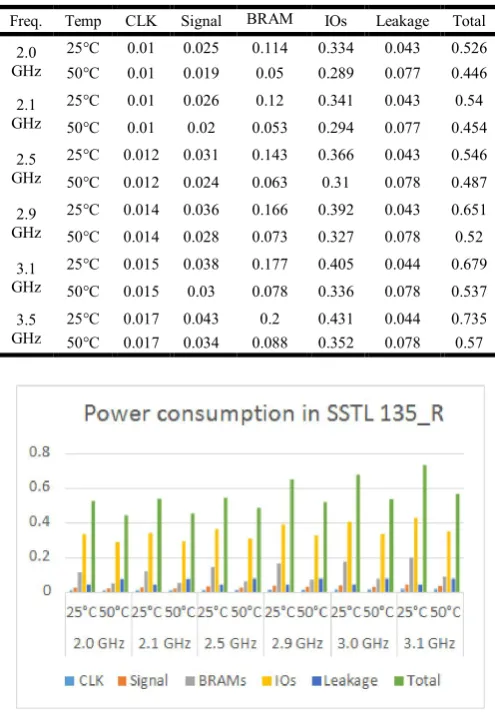
B. Power Dissipation with SSTL 135_R I/O Standard
Table 2 shows the power consumption by HSTL 135_R I/O standard at different operating frequencies. From Table 2 it is clear that if we operate our device at 2.0 GHz rather than 3.1 GHz then we can save 41.17% clock power, 41.8% signal power, 43% BRAMs power, 22.55% IO power and total we can save 28.43% power consumption operating at 25°C and if it is operated at 50°C then we can further save 15.2% power on same frequency i.e. 2.0 GHz.
Table 2. Power Consumption of SSTL 135_R I/O standard
Freq. Temp CLK Signal BRAM
s
IOs Leakage Total
2.0 GHz
25°C 0.01 0.025 0.114 0.334 0.043 0.526
50°C 0.01 0.019 0.05 0.289 0.077 0.446
2.1 GHz
25°C 0.01 0.026 0.12 0.341 0.043 0.54
50°C 0.01 0.02 0.053 0.294 0.077 0.454
2.5 GHz
25°C 0.012 0.031 0.143 0.366 0.043 0.546
50°C 0.012 0.024 0.063 0.31 0.078 0.487
2.9 GHz
25°C 0.014 0.036 0.166 0.392 0.043 0.651
50°C 0.014 0.028 0.073 0.327 0.078 0.52
3.1 GHz
25°C 0.015 0.038 0.177 0.405 0.044 0.679
50°C 0.015 0.03 0.078 0.336 0.078 0.537
3.5 GHz
25°C 0.017 0.043 0.2 0.431 0.044 0.735
50°C 0.017 0.034 0.088 0.352 0.078 0.57
Figure 6. Power Dissipation versus Frequency on SSTL 135_R
C. Power Dissipation with SSTL 15 I/O Standard
Table 3 shows the power consumption by HSTL 15 I/O standard at different operating frequencies.
25°C and if it is operated at 2.5GHz and if temperature is changed from 25°C to 50°C then we can further save 21.81% power on same frequency.
Table 3. Power Consumption of SSTL 15 I/O standard
Freq .
Temp CLK Signal BRAM
s
IOs Leakage Total
2.0 GHz
25°C 0.01 0.026 0.144 0.504 0.044 0.698
50°C 0.01 0.021 0.05 0.407 0.078 0.566
2.1 GHz
25°C 0.01 0.027 0.12 0.516 0.044 0.717
50°C 0.01 0.022 0.053 0.414 0.078 0.577
2.5 GHz
25°C 0.012 0.032 0.143 0.561 0.044 0.793
50°C 0.012 0.026 0.063 0.44 0.079 0.62
2.9 GHz
25°C 0.014 0.038 0.116 0.607 0.044 0.869
50°C 0.014 0.03 0.073 0.466 0.079 0.662
3.1 GHz
25°C 0.015 0.04 0.177 0.63 0.044 0.869
50°C 0.015 0.032 0.078 0.479 0.079 0.684
3.5 GHz
25°C 0.017 0.045 0.2 0.675 0.045 0.982
50°C 0.017 0.036 0.088 0.506 0.079 0.726
Figure 7. Power Dissipation versus Frequency on SSTL 135
D. Power Dissipation with SSTL 15_R I/O Standard
Table 4 shows power consumption by SSTL 15_R I/O standard based RAM operating at 25°C and 50°C and at different operating frequencies.
Table 4. Power Consumption of SSTL 15_R I/O standard
Freq. Tem
p
CLK Signal BRAMs IOs Leakage Total
2.0 GHz
25°C 0.01 0.025 0.144 0.343 0.043 0.535
50°C 0.01 0.019 0.05 0.297 0.077 0.454
2.1 25°C 0.01 0.026 0.12 0.35 0.043 0.549
50°C 0.01 0.02 0.053 0.302 0.078 0.463
2.5 25°C 0.012 0.031 0.143 0.376 0.044 0.605
50°C 0.012 0.024 0.063 0.319 0.078 0.496
2.9 25°C 0.014 0.036 0.166 0.402 0.044 0.661
50°C 0.014 0.028 0.073 0.336 0.078 0.529
3.1 25°C 0.015 0.038 0.177 0.415 0.044 0.689
50°C 0.015 0.03 0.078 0.344 0.078 0.546
3.5 GHz
25°C 0.017 0.043 0.2 0.441 0.044 0.745
50°C 0.017 0.034 0.088 0.361 0.078 0.579
As shown in Table-4 the clock power remains same at 2.0 GHz and 2.1 GHz but increases by 16.66% at 2.5 GHz. The power consumption operating at 2.0 GHz increases by 2.55% at 2.1 GHz, 11.5% at 2.5 GHz, 19.06% at 2.9 GHz, 22.35% at 3.1 GHz and 28.18 at 3.5 GHz. We can save 39.06% total power if we change the parameters from 3.5 GHz and 25°C to 2.0 GHz and 50°C.
Figure 8. Power Dissipation versus Frequency on SSTL 15_R
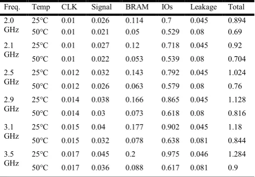
E. Power Dissipation with SSTL 18_I I/O Standard
Table 5 shows power consumption by SSTL 18_R I/O standard based RAM operating at 25°C and 50°C and at different operating frequencies.
Table 5. Power Consumption of SSTL 18 IO_I standard
Freq. Temp CLK Signal BRAM
s
IOs Leakage Total
2.0 GHz
25°C 0.01 0.026 0.114 0.7 0.045 0.894
50°C 0.01 0.021 0.05 0.529 0.08 0.69
2.1 GHz
25°C 0.01 0.027 0.12 0.718 0.045 0.92
50°C 0.01 0.022 0.053 0.539 0.08 0.704
2.5 GHz
25°C 0.012 0.032 0.143 0.792 0.045 1.024
50°C 0.012 0.026 0.063 0.579 0.08 0.76
2.9 GHz
25°C 0.014 0.038 0.166 0.865 0.045 1.128
50°C 0.014 0.03 0.073 0.618 0.08 0.816
3.1 GHz
25°C 0.015 0.04 0.177 0.902 0.045 1.18
50°C 0.015 0.032 0.078 0.638 0.081 0.844
3.5 GHz
25°C 0.017 0.045 0.2 0.975 0.046 1.284
50°C 0.017 0.036 0.088 0.617 0.081 0.9
Figure 9. Power Dissipation versus Frequency on SSTL 18_I
F. Power Dissipation with SSTL 18_II I/O Standard
In this work, our aim is to reduce the power consumption and make our system faster, most power efficient and cost-effective. In this experiment we analyze the power consumption RAM memory circuit based on SSTL 18_II I/O standard.
Table 6. Power Consumption of SSTL 18 IO_II standard
Freq .
Temp CLK Signal BRAMs IOs Leakage Total
2.0 GHz
25°C 0.01 0.026 0.114 0.836 0.045 1.031
50°C 0.01 0.021 0.05 0.631 0.08 0.792
2.1 GHz
25°C 0.01 0.027 0.12 0.858 0.045 1.06
50°C 0.01 0.022 0.053 0.643 0.08 0.808
2.5 GHz
25°C 0.012 0.032 0.143 0.944 0.045 1.177
50°C 0.012 0.026 0.063 0.688 0.081 0.87
2.9 GHz
25°C 0.014 0.038 0.166 1.031 0.046 1.294
50°C 0.014 0.03 0.073 0.074 0.081 0.932
3.1 GHz
25°C 0.015 0.04 0.177 1.074 0.046 1.352
50°C 0.015 0.032 0.078 0.757 0.082 0.963
3.5 GHz
25°C 0.017 0.045 0.2 1.16 0.046 1.469
50°C 0.017 0.036 0.088 0.802 0.802 1.026
Figure 10. Power Dissipation versus Frequency on SSTL 18_II
From Table 6 it is clear that SSTL 18_II consumes 1.031W power at 2.0 GHz frequency at 25°C and 0.792W at 50°C which is 23.18% less. Power consumption increases by 2.73% at 2.1 GHz at, 12.40% at 2.5 GHz, 20.32% at 2.9 GHz, 23.74% at 3.1 GHz and 29.81% at 3.5 GHz operating at 25°C.
Power analysis of the memory circuit with different i/o standard
This section is based on the analysis of power consumption by the memory circuit based on all six SSTL I/O standard on same operating frequency and temperature. In order to find most efficient RAM design, the circuit based on all six SSTL I/O standard is compared at six different operating frequencies.
A. Power consumption at 2.0 GHz frequency.
In this work, our objective is to reduce the power consumption and make our system faster, most power efficient. In this section we have analyzed the power consumption by the RAM circuit at 2.0 GHz operating frequency based on different SSTL logic standards as shown in Table 7.
Table 7. Power Consumption at 2.0 GHz
SSTL Temp CLK Signal BRAMs IOs Leakage Total
SSTL 135
25°C 0.01 0.026 0.114 0.483 0.044 0.677
50°C 0.01 0.021 0.05 0.389 0.078 0.547
SSTL 135_R
25°C 0.01 0.025 0.114 0.334 0.043 0.526
50°C 0.01 0.019 0.05 0.289 0.077 0.446
SSTL 15
25°C 0.01 0.026 0.114 0.504 0.044 0.698
50°C 0.01 0.021 0.05 0.407 0.078 0.566
SSTL 15_R
25°C 0.01 0.025 0.114 0.343 0.043 0.535
50°C 0.01 0.019 0.05 0.297 0.077 0.454
SSTL 18_I
25°C 0.01 0.026 0.114 0.7 0.045 0.894
50°C 0.01 0.021 0.05 0.529 0.08 0.69
SSTL 18_II
25°C 0.01 0.026 0.114 0.836 0.045 1.031
50°C 0.01 0.021 0.05 0.631 0.08 0.792
Figure 11. Power Dissipation at 2.0 GHz frequency
From the Table 7 it is clear that there is no change in the
clockpower, signal power and BRAMs power but in case of
SSTL 135_R and SSTL 15_R signal power decreases from
50°C. The I/O power changes with change in frequency. The power consumption of the RAM circuit is 1.031W with SSTL 18_II I/O standard and it can be reduced by 34.33%, 48.98%, 32.29%, 48.10% and 13.28% with SSTL 135, SSTL 135_R, SSTL 15, SSTL 15_R and SSTL 18_I respectively at 2.0 GHz frequency as shown in Table 7.
B. Power Consumption at 2.1 GHz frequency
In this work, our objective is to reduce the power consumption and make our system faster, most power efficient. In this section we have analyzed the power consumption by the RAM circuit at 2.1 GHz operating frequency based on different SSTL logic standards as shown in Table 8.
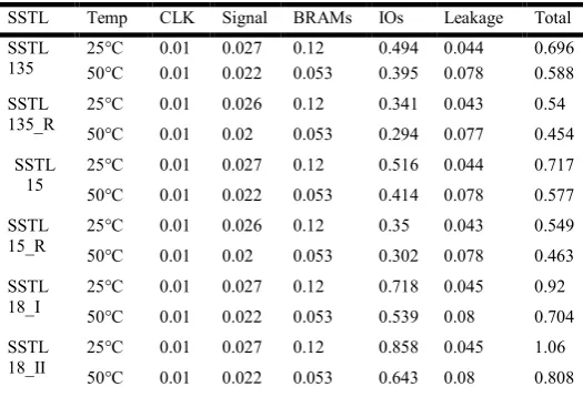
Table 8. Power Consumption at 2.1 GHz
SSTL Temp CLK Signal BRAMs IOs Leakage Total
SSTL 135
25°C 0.01 0.027 0.12 0.494 0.044 0.696
50°C 0.01 0.022 0.053 0.395 0.078 0.588
SSTL 135_R
25°C 0.01 0.026 0.12 0.341 0.043 0.54
50°C 0.01 0.02 0.053 0.294 0.077 0.454
SSTL 15
25°C 0.01 0.027 0.12 0.516 0.044 0.717
50°C 0.01 0.022 0.053 0.414 0.078 0.577
SSTL 15_R
25°C 0.01 0.026 0.12 0.35 0.043 0.549
50°C 0.01 0.02 0.053 0.302 0.078 0.463
SSTL 18_I
25°C 0.01 0.027 0.12 0.718 0.045 0.92
50°C 0.01 0.022 0.053 0.539 0.08 0.704
SSTL 18_II
25°C 0.01 0.027 0.12 0.858 0.045 1.06
50°C 0.01 0.022 0.053 0.643 0.08 0.808
From the Table 8 it is clear that there is no change in the clock power, signal power and BRAMs power but in case of SSTL 135_R and SSTL 15_R signal power decreases from 0.027W to 0.026W at 25°C and from 0.022W to 0.02W at 50°C. The I/O power changes with change in frequency. The power consumption of the RAM circuit is 1.06W with SSTL 18_II I/O standard and it can be reduced by 34.33%, 49.05%, 32.35%, 48.20% and 13.20% with SSTL 135, SSTL 135_R, SSTL 15, SSTL 15_R and SSTL 18_I respectively at 2.1 GHz frequency and if temperature is 50°C then total power saving is 57.16% with SSTL 135_R I/O standard.
Figure 12. Power Dissipation at 2.1 GHz frequency
C. Power Consumption at 2.5 GHz frequency
In this work, our objective is to reduce the power consumption and make our system faster, most power efficient. In this section we have analyzed the power consumption by the RAM circuit at 2.5 GHz operating frequency based on different SSTL logic standards as shown in Table 9.
Table 9. Power Consumption at 2.5 GHz
SSTL Temp CLK Signal BRAMs IOs Leakage Total
SSTL 135
25°C 0.012 0.032 0.143 0.539 0.044 0.72
50°C 0.012 0.026 0.063 0.421 0.078 0.6
SSTL 135_R
25°C 0.012 0.031 0.143 0.366 0.043 0.546
50°C 0.012 0.024 0.063 0.31 0.078 0.487
SSTL 15
25°C 0.012 0.032 0.143 0.561 0.044 0.793
50°C 0.012 0.026 0.063 0.44 0.079 0.62
SSTL 15_R
25°C 0.012 0.031 0.143 0.376 0.044 0.605
50°C 0.012 0.024 0.063 0.319 0.078 0.496
SSTL 18_I
25°C 0.012 0.032 0.143 0.792 0.045 1.024
50°C 0.012 0.026 0.063 0.579 0.08 0.76
SSTL 18_II
25°C 0.012 0.032 0.143 0.944 0.045 1.177
50°C 0.012 0.026 0.063 0.688 0.081 0.87
From the Table 9 it is clear that there is no change in the clock power, signal power and BRAMs power but in case of SSTL 135_R and SSTL 15_R signal power decreases from 0.032W to 0.031W at 25°C and from 0.026W to 0.024W at 50°C. The I/O power changes with change in frequency. The power consumption of the RAM circuit is 1.177W with SSTL 18_II I/O standard and it can be reduced by 38.82%, 53.61%, 32.62%, 48.59% and 12.99% with SSTL 135, SSTL 135_R, SSTL 15, SSTL 15_R and SSTL 18_I respectively at 2.5 GHz frequency and if temperature is 50°C then total power saving is 58.62% with SSTL 135_R I/O standard.
Figure 13. Power Dissipation at 2.5 GHz frequency
D. Power Consumption at 2.9 GHz frequency
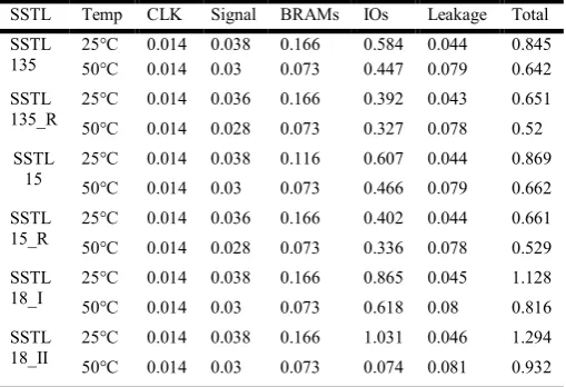
From the Table 10 it is clear that there is no change in the clock power, signal power and BRAMs power but in case of SSTL 135_R and SSTL 15_R signal power decreases from 0.038W to 0.036W at 25°C and from 0.003W to 0.028W at 50°C. The I/O power changes with change in frequency. The power consumption of the RAM circuit is 1.294W with SSTL 18_II I/O standard and it can be reduced by 34.69%, 49.69%, 32.84%, 48.91% and 12.82% with SSTL 135, SSTL 135_R, SSTL 15, SSTL 15_R and SSTL 18_I respectively at 2.9 GHz frequency and if temperature is 50°C then total power saving is 59.81% with SSTL 135_R I/O standard.
Figure 14. Power Dissipation at 2.9 GHz frequency
E. Power Consumption at 3.1 GHz frequency
In this work, our objective is to reduce the power consumption and make our system faster, most power efficient. In this section we have analyzed the power consumption by the RAM circuit at 3.1 GHz operating frequency based on different SSTL logic standards as shown in Table 11.
From the Table 11 it is clear that there is no change in the clock power, signal power and BRAMs power but in case of SSTL 135_R and SSTL 15_R signal power decreases from 0.04W to 0.038W at 25°C and from 0.030W to 0.03W at 50°C. The I/O power changes with change in frequency. The power consumption of the RAM circuit is 1.352W with SSTL
18_II I/O standard and it can be reduced by 34.68%, 49.77%, 35.72%, 49.03% and 12.72% with SSTL 135, SSTL 135_R, SSTL 15, SSTL 15_R and SSTL 18_I respectively at 3.1 GHz frequency and if temperature is 50°C then total power saving is 60.28% with SSTL 135_R I/O standard.
Table 11. Power Consumption at 3.1 GHz
SSTL Temp CLK Signal BRAMs IOs Leakage Total
SSTL 135
25°C 0.015 0.04 0.177 0.606 0.044 0.883
50°C 0.015 0.032 0.078 0.459 0.079 0.633
SSTL 135_R
25°C 0.015 0.038 0.177 0.405 0.044 0.679
50°C 0.015 0.03 0.078 0.336 0.078 0.537
SSTL 15
25°C 0.015 0.04 0.177 0.63 0.044 0.869
50°C 0.015 0.032 0.078 0.479 0.079 0.684
SSTL 15_R
25°C 0.015 0.038 0.177 0.415 0.044 0.689
50°C 0.015 0.03 0.078 0.344 0.078 0.546
SSTL 18_I
25°C 0.015 0.04 0.177 0.902 0.045 1.18
50°C 0.015 0.032 0.078 0.638 0.081 0.844
SSTL 18_II
25°C 0.015 0.04 0.177 1.074 0.046 1.352
50°C 0.015 0.032 0.078 0.757 0.082 0.963
Figure 15. Power Dissipation at 3.1 GHz frequency
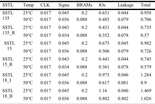
F. Power Consumption at 3.5 GHz frequency
In this work, our objective is to reduce the power consumption and make our system faster, most power efficient. In this section we have analyzed the power consumption by the RAM circuit at 3.5 GHz operating frequency based on different SSTL logic standards as shown in Table 12.
From the Table 12 it is clear that there is no change in the clock power, signal power and BRAMs power but in case of SSTL 135_R and SSTL 15_R signal power decreases from 0.045W to 0.043W at 25°C and from 0.036W to 0.034W at 50°C. The I/O power changes with change in frequency. The power consumption of the RAM circuit is 1.469W with SSTL 18_II I/O standard and it can be reduced by 34.78%, 49.96%, 33.15%, 49.28% and 12.59% with SSTL 135, SSTL 135_R, SSTL 15, SSTL 15_R and SSTL 18_I respectively at 3.1 GHz frequency and if temperature is 50°C then total power saving is 61.19% with SSTL 135_R I/O standard.
Table 10. Power Consumption at 2.9 GHz
SSTL Temp CLK Signal BRAMs IOs Leakage Total
SSTL 135
25°C 0.014 0.038 0.166 0.584 0.044 0.845
50°C 0.014 0.03 0.073 0.447 0.079 0.642
SSTL 135_R
25°C 0.014 0.036 0.166 0.392 0.043 0.651
50°C 0.014 0.028 0.073 0.327 0.078 0.52
SSTL 15
25°C 0.014 0.038 0.116 0.607 0.044 0.869
50°C 0.014 0.03 0.073 0.466 0.079 0.662
SSTL 15_R
25°C 0.014 0.036 0.166 0.402 0.044 0.661
50°C 0.014 0.028 0.073 0.336 0.078 0.529
SSTL 18_I
25°C 0.014 0.038 0.166 0.865 0.045 1.128
50°C 0.014 0.03 0.073 0.618 0.08 0.816
SSTL 18_II
25°C 0.014 0.038 0.166 1.031 0.046 1.294
Table 12. Power Consumption at 3.5 GHz
SSTL Temp CLK Signa
l
BRAMs IOs Leakage Total
SSTL 135
25°C 0.017 0.045 0.2 0.651 0.044 0.958
50°C 0.017 0.036 0.088 0.485 0.079 0.706
SSTL 135_R
25°C 0.017 0.043 0.2 0.431 0.044 0.735
50°C 0.017 0.034 0.088 0.352 0.078 0.57
SSTL 15
25°C 0.017 0.045 0.2 0.675 0.045 0.982
50°C 0.017 0.036 0.088 0.506 0.079 0.726
SSTL 15_R
25°C 0.017 0.043 0.2 0.441 0.044 0.745
50°C 0.017 0.034 0.088 0.361 0.078 0.579
SSTL 18_I
25°C 0.017 0.045 0.2 0.975 0.046 1.284
50°C 0.017 0.036 0.088 0.617 0.081 0.9
SSTL 18_II
25°C 0.017 0.045 0.2 1.16 0.046 1.469
50°C 0.017 0.036 0.088 0.802 0.802 1.026
Conclusions
The conclusion from the whole work that we have done is basically that we can save approximately 60% power consumption of our RAM circuit operating on same frequency if we go for SSTL 135_R I/O standard based design in place of SSTL 18_II and we can save total 69.63% power if operating frequency is decreased to 2.0 GHz from 3.5 GHz and operating temperature is changed from 25°C to 50°C with SSTL 135_R in place of SSTL 18_II I/O standard.
Future Scope
In this work, we are using SSTL IO standards with feature size 28nm in energy efficient design of RAM. In future, we can go for other memory circuits like register, counter, ROM and CAM. There is also wide scope to design energy efficient memory using different IO standards like Transistor-Transistor Logic, mobile DDR, High Speed Unterminated Logic, High Speed Transceiver Logic, Low Voltage Complementary Transistor-Transistor Logic, Gunning Transceiver Logic and Peripheral Component interconnect. Now, our target design is 28nm technology based Artix-7 FPGA. We can migrate to 3-D IC, System on Chips (SoCs) and other PLDs and re-implement same memory on that. In future, we shall design high speed memory that will be able to operate with frequency in range of 1 THz and beyond.
REFERENCES
Kumar, T., Pandey, B. Das, T. and Rahman, MA. 2013. "SSTL Based Green Image ALU Design on different FPGA", IEEE International conference on Green Computing, Communication and Conservation of Energy(ICGCE), 12-14 December, 2013.
Das, T., Pandey, B. Kumar, T. Kumar, P. and Kumar, L. 2014. “Simulation of SSTL IO Standard Based Power Optimized Parallel Integrator Design on FPGA”, IEEE International Conference on Robotics and Emerging Allied Technologies in Engineering (iCREATE), National University of Sciences and Technology (NUST), Islamabad, Pakistan Islam, S. M. M., M. Janmaijaya, T. Kumar, MA. Rahman and
B. Pandey, 2013. “SSTL I/O Standard based Simulation of Energy Efficient VCM on FPGA”, IEEE International Conference on Communication and Computer Vision (ICCCV), 20-21.
Meenakshi Bansal, Neha Bansal, Rishita Saini, Bishwajeet Pandey, Lakshay Kalra, D. M. Akbar Hussain, 2014. “SSTL I/O Standard Based Environment Friendly Energy
Efficient ROM Design on FPGA”, Environmental Friendly
Energies and Applications (EFEA), 2014 3rd International Symposium on. IEEE.
Lerong Cheng, Fei Li, Yan Lin, Phoebe Wong, and Lei H, “Device and Architecture Cooptimization for FPGA Power Reduction”, Ieee transactions on Computeraided design of integrated circuits and systems, vol. 26, no. 7, July 2007.
Wai-Kei Mak, “I/O Placement for FPGAs With Multiple I/O Standards”, Ieee Transactions on Computeraided design of
integrated circuits and systems, vol. 23, no. 2, February 2004.
Fatima Zahra Tazi, Claude Thibeault, Yvon Savaria, Simon Pichette, and Yves Audet,” On Extra Delays Affecting I/O Blocks of an SRAM-Based FPGA Due to
Ionizing Radiation”, IEEE Transactions on Nuclear
Science, vol. 61, no. 6, December 2014.
Herrera-Alzu and M. López-Vallejo, “Design Techniques for Xilinx Virtex FPGA Configuration Memory Scrubbers”, IEEE transactions on Nuclear Science, vol. 60, no. 1, February 2013.
Vece, G.B. Contin, M., and S. Orcioni, 2015 “Transaction-level power analysis of VLSI digital systems”, Elsevier, Integration the VLSI Journal 50 116-126.
Nandha Kumar, T. and Fabrizio Lombardi, “A Novel Heuristic Method for Application-Dependent Testing of a SRAMBased FPGA Interconnect”, IEEE transactions on Computers, vol. 62, no. 1, January 2013.