FPGA IMPLEMENTATION OF FAST ADDER USING
CARRY SAVE RECONFIGURABLE ADDER
1
Ms. Parul Katiyar,
2Ms. Shalini singh
1,2
Department of Electronics and Communication Engineering, IPEC, (India)
ABSTRACT
This paper shows how to implement carry-save arithmetic with reconfigurable adder. The architecture of the
adder is such that it should add two operands fast. The adder will be design as an IP (Intellectual Property)
core. The reconfigurable adder is then implementing on FPGA, Spartan 3E series board. A reconfigurable
system is one that changes its form in order to alter its function. For it to be more than “configurable” it must
be possible to change it either whilst it is in use, or by taking it out of use for a short time.
Keywords: Adder, CSA, FPGA, Reconfigurable.
I. INTRODUCTION
Arithmetic operations play an important role in various digital systems such as computers, process controllers,
signal processors computer graphics and image processing. Recent advances in technologies for integrated
circuits make large scale arithmetic circuits suitable for VLSI implementation [1]. However, arithmetic operations
still suffer from known problems including limited number of bits, propagation time delay, and circuit
complexity. Now, the flexibility of field programmable gate arrays (FPGAs) allows the rapid development of
high performance custom hardware. By selecting arithmetic algorithms suited to the FPGA technology and
subsequently applying optimal mapping strategies, high performance FPGA implementations can be developed
[2].
This paper discusses the proposed reconfigurable adder & also its implementation on FPGA board for physical
verification.
II. CARRY-SAVE ADDER (CSA)
Using carry save addition, the delay can be reduced further still. The idea is to take 3 numbers that we want to
add together, x + y + z, and convert it into 2 numbers c + s such that x + y + z = c + s, and do this in O(1) time.
The reason why addition cannot be performed in O(1) time is because the carry information must be propagated.
In carry save addition, we refrain from directly passing on the carry information until the very last step. We will
first illustrate the general concept with a example of decimal numbers.
To add three numbers, we typically align the three operands, and then proceed column by column in the same
fashion that we perform addition with two numbers. The three digits in a column are added, and any overflow,
say carry goes into the next column. Observe that when there is any non-zero carry, we are really adding four
digits (the digits of x,y and z, plus the carry).
Carry: 1 1 2 1
y: 3 8 1 7 2
z: + 2 0 5 8 7
sum: 7 1 1 0 4
The carry save approach breaks this process down into two steps. The first is to compute the sum ignoring any
carries:
x: 1 2 3 4 5
y: 3 8 1 7 2
z: + 2 0 5 8 7
s: 6 0 9 9 4
Each si is equal to the sum of xi + yi + zi modulo 10. Now, separately, we can compute the carry on a column
by column basis:
x: 1 2 3 4 5
y: 3 8 1 7 2
z: + 2 0 5 8 7
c: 1 0 1 1
In this case, each ci is the sum of the bits from the previous column divided by 10 (ignoring any remainder).
Another way to look at it is that any carry over from one column gets put into the next column. Now, we can
add together c and s, and we’ll verify that it indeed is equal to x + y + z:.
A carry save adder (CSA) is very fast where there is no carry propagation within each CSA cell. It is only the
final recombination of the final carry and sum requires a carry propagating addition [4] that simply outputs the
carry bits instead of propagating them to the side. Since it save all the carries from all the adds to the last stage
and do one Carry Look-ahead Adder (CLA) or Ripple Carry Adder (RCA) at the end. Thus, using carry-save
adders avoids carry propagation and will result in a higher throughput. Minimum adder integer multipliers using
Carry Save Adder [3]. The CSA design automatically avoids the delay in the carryout bits [5]. It is well known
that carry-save arithmetic is a useful technique in the implementation of high-speed arithmetic functions. Carry
save adder used widely in design because carry save addition saves logic and time
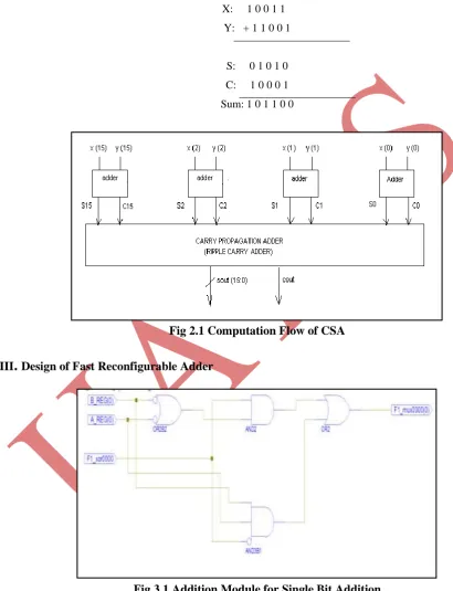
Basically, carry save adder is used to compute sum of three or more n-bit binary numbers. Carry save adder is
same as a full adder. But as shown in figure.10, here we are computing sum of two 16-bit binary numbers, so we
take 16 half adders at first stage instead of using 16 full adders. Therefore, carry save unit consists of 16 half
adders, each of which computes single sum and carry bit based only on the corresponding bits of the two input
numbers. Let x and y are two 16 bit numbers and produces partial sum and carry as s and c as shown below:
Si = Xi XOR Yi
Ci = Xi AND Yi
Finally, a ripple carry adder is used to add these two together and computing the resulting sum.
The addition is explained using an example. Two operands of 4 bits size is added partially with their carry added
in the end. The addition of carry in the end saves the time needed to propagate the carry that is used in
conventional adder.
X: 1 0 0 1 1
Y: + 1 1 0 0 1
S: 0 1 0 1 0
C: 1 0 0 0 1
Sum: 1 0 1 1 0 0
Fig 2.1 Computation Flow of CSA
III
.
Design of Fast Reconfigurable Adder
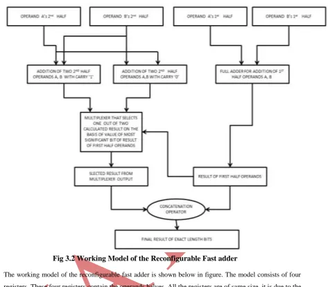
Fig 3.2 Working Model of the Reconfigurable Fast adder
The working model of the reconfigurable fast adder is shown below in figure. The model consists of four
registers. These four registers contain the operands halves. All the registers are of same size, it is due to the
reason that the operands are divided into two halves of equal size.
The model consist of operands A and B divided into two equal halves the first two halves as shown in the
figure is added separately & its most significant bit is then used as the select signal for the multiplexer that
select the already calculated addition result for the next halves. In the end there is a concatenation operator
that concatenates the two final halves of the result to finally have the result of addition of two operands in a
register.
The addition units shown in the above figure are based on the concept of calculating the two possible
results i.e. theone without carry & the one with carry, thus eliminating the delay due to carry propagation.
So in this way the entire addition operation is carried out using the carry save addition algorithm & using
the same concept for even the single bit addition operation. By performing addition operation this way we
achieved performance improvement as compare to the other adder types.
4.1 Logic Verification
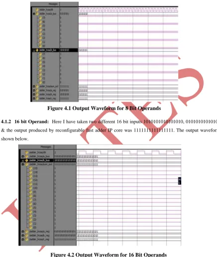
4.1.1 8 bit Operand: I have taken two different 8 bit inputs 10101010, 01010101 & the output produced by
Reconfigurable fast adder IP core was 11111111. The output waveform shown below.
Figure 4.1 Output Waveform for 8 Bit Operands
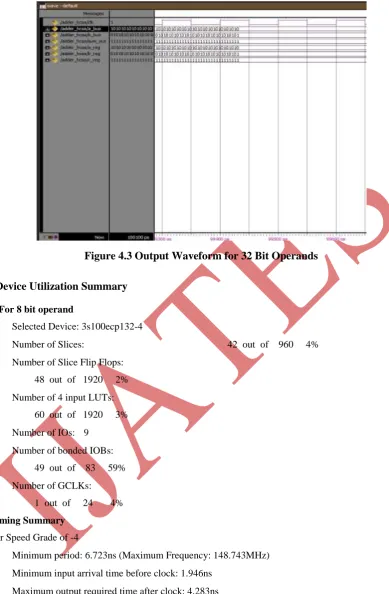
4.1.2 16 bit Operand: Here I have taken two different 16 bit inputs 1010101010101010, 01010101010101
& the output produced by reconfigurable fast adder IP core was 1111111111111111. The output waveform
shown below.
Figure 4.2 Output Waveform for 16 Bit Operands
4.1.3 32 bit Operand: Here I have taken two different 32 bit inputs
10101010101010101010101010101010, 0101010101010101010101010101 & the output produced by
reconfigurable fast adder IP core was 11111111111111111111111111111111. The output waveformshown
Figure 4.3 Output Waveform for 32 Bit Operands
4.2. Device Utilization Summary
4.2.1 For 8 bit operand
Selected Device: 3s100ecp132-4
Number of Slices: 42 out of 960 4%
Number of Slice Flip Flops:
48 out of 1920 2%
Number of 4 input LUTs:
60 out of 1920 3%
Number of IOs: 9
Number of bonded IOBs:
49 out of 83 59%
Number of GCLKs:
1 out of 24 4%
Timing Summary
For Speed Grade of -4
Minimum period: 6.723ns (Maximum Frequency: 148.743MHz)
Minimum input arrival time before clock: 1.946ns
Maximum output required time after clock: 4.283ns
4.2.2 For 16 bit operand
48 out of 1920 2%
Number of 4 input LUTs:
60 out of 1920 3%
Number of IOs: 49
Number of bonded IOBs:
49 out of 83 59%
Number of GCLKs: 1 out of 24 4%
Timing Summary
For Speed Grade of -4
Minimum period: 6.723ns (Maximum Frequency: 148.743MHz)
Minimum input arrival time before clock: 1.946ns
Maximum output required time after clock: 4.283ns
4.2.3 For 32 bit operand
Selected Device: 3s100ecp132-4
Number of Slices: 91 out of 960 9%
Number of Slice Flip Flops:
96 out of 1920 5%
Number of 4 input LUTs:
126 out of 1920 6%
Number of IOs: 97
Number of bonded IOBs:
97 out of 83 116%
Number of GCLKs: 1 out of 24 4%
Timing Summary
For Speed Grade of -4
Minimum period: 9.625ns (Maximum Frequency: 103.896MHz)
Minimum input arrival time before clock: 1.946ns
Maximum output required time after clock: 4.283ns
V. CONCLUSION
In this work, a reconfigurable fast adder was presented. It can be reconfigured in terms of bit width of the
operands provided that the degree of operands is 2. Its architecture comprises of addition units that does addition
operation of individual bit by calculating the result in advance in the presence & as well as in the absence of
carry, thus eliminating the delay due to carry propagation.
[1] Chao Cheng; Parhi and K.K. “High-Throughput VLSI Architecture for FFT Computation”, IEEE
Transactions on Volume 54, Issue 10, Page 863 – 867, October 2007.
[2] A. Avizienis, “Signed-Digit Number Representation for Fast Parallel Arithmetic, ”IRE Transaction
Electron. Comp., EC-10, pp. 389-400, 1961
[3] Oscar Gustafssoiz, Herzrik Olilssoii, arid Lars Wanhammar, (2004). Minimum adder integer multipliers
using Carry Save Adder, Proc. IEEE Int. Symp. Circuits Syst., Sydney, Australia
[4] John Cooley, EDA & ASIC Design Consultant in Synopsys, Verilog, VHDL and numerous Design
Methodologies, University of Moratuwa, Sri Lanka Department of Computer Science & Engineering.
[5] Chetana Nagendra, Irwin M. J., Owens R. M., (1996). Area-Time-Power Tradeoffs in Parallel Adders, IEEE
Transactions on Circuits and Systems, Vol.43.
[6] James Levy, Jabulani Nyathi, and Jos´e Delgado-Frias, (2005). High- Performance Parallel Addition Using
Hybrid Wave-Pipelining, IEEE Transaction of EECS.
[7] Altera University Program UP2 Education kit user guide (2004). Vol. 3.1.
[8] Prof. Dr.-Ing. Wolfgang Kunz, Technische Universität Kaiserslautern, (2005), Algoritmic Design of
Arithmetic Circuit, www-eda.eit.uni-kl.de.