440 |
P a g e
FPGA IMPLEMENTATION OF AES ALGORITHM
S.A. Annadate
1, Nitin Ram Chavan
2 1,2Electronics and Telecommunication Dept, J N Collage of engineering Aurangabad, (India)
ABSTRACT
Advanced Encryption Standard (AES)is an FIPS approved cryptographic algorithm that can be used to protect electronic data. The AES can be programmed in software or built with pure hardware. However FPGA offer a quicker and more customizable solution. This paper presents the AES algorithm with regard to FPGA and the Very High Speed Integrated Circuit Hardware Description language (VHDL). ModelSim SE PLUS 5.7g software is used for simulation and optimization of the synthesizable VHDL code. Synthesizing and implementation (i.e. Translate, Map and Place and Route) of the code is carried out on Xilinx - Project Navigator, ISE 8.2i suite. All the transformations of both Encryption and Decryption are simulated using an iterative design approach in order to minimize the hardware consumption. Xilinx XC3S400 device of Spartan Family is used for hardware evaluation. This paper proposes a method to integrate the AES encrypter and the AES decrypter. This method can make it a very low-complexity architecture, especially in saving the hardware resource in implementing the AES (Inv) Sub Bytes module and (Inv) Mix columns module etc Besides, the architecture can still deliver a high data rate that suited for hardware-critical applications, such as smart card, PDA, and mobile phone etc.
Keywords: AES, Encryption Decryption, FPGA, VHDL,
Xilinx.I INTRODUCTION
1.1 General
Cryptography, often called encryption, is the practice of creating and using a cryptosystem or cipher to prevent
all but the intended recipient(s) from reading or using the information or application encrypted. A cryptosystem
is a technique used to encode a message. The recipient can view the encrypted message only by decoding it with
the correct algorithm and keys. Cryptography is used primarily for communicating sensitive material across
computer networks[3]. The process of encryption takes a clear-text document and applies a key and a
mathematical algorithm to it, converting it into crypto-text. In crypto-text, the document is unreadable unless the
reader possesses the key that can undo the encryption. In 1997 the National Institute of Standards and
Technology (NIST), a branch of the US government, started a process to identify a replacement for the Data
Encryption Standard (DES). It was generally recognized that DES was not secure because of advances in
computer processing power. The goal of NIST was to define a replacement for DES that could be used for
non-military information security applications by US government agencies. Of course, it was recognized that
441 |
P a g e
generally adopted as a commercial standard. The NIST invited cryptography and data security specialists from
around the world to participate in the discussion and selection process. Five encryption algorithms were adopted
for study. Through a process of consensus the encryption algorithm proposed by the Belgium cryptographers
Joan Daeman and Vincent Rijmen was selected. Prior to selection Daeman and Rijmen used the name Rijndael
(derived from their names) for the algorithm[3]. After adoption the encryption algorithm was given the name
Advanced Encryption Standard (AES) which is in common use today. In 2000 the NIST formally adopted the
AES encryption algorithm and published it as a federal standard under the designation 197. The full
FIPS-197 standard is available on the NIST web site (see the Resources section below). As expected, many providers
of encryption software and hardware have incorporated AES encryption into their products[1].
The AES encryption algorithm is a block cipher that uses an encryption key and a several rounds of encryption.
A block cipher is an encryption algorithm that works on a single block of data at a time. In the case of standard
AES encryption the block is 128 bits, or 16 bytes, in length. The term “rounds” refers to the way in which the
encryption algorithm mixes the data re-encrypting it ten to fourteen times depending on the length of the key.
This is described in the Wikipedia article on AES encryption. The AES algorithm itself is not a computer
program or computer source code. It is a mathematical description of a process of obscuring data. A number of
people have created source code implementations of AES encryption, including the original authors[6].
AES encryption uses a single key as a part of the encryption process. The key can be 128 bits (16 bytes), 192
bits (24 bytes), or 256 bits (32 bytes) in length. The term 128-bit encryption refers to the use of a 128-bit
encryption key. With AES both the encryption and the decryption are performed using the same key. This is
called a symmetric encryption algorithm. Encryption algorithms that use two different keys, a public and a
private key, are called asymmetric encryption algorithms. An encryption key is simply a binary string of data
used in the encryption process. Because the same encryption key is used to encrypt and decrypt data, it is
important to keep the encryption key a secret and to use keys that are hard to guess. Some keys are generated by
software used for this specific task. Another method is to derive a key from a pass phrase. Good encryption
systems never use a pass phrase alone as an encryption key.NIST was aware of side channel attacks when
evaluating all the finalists[2]. Comparing the Rijndael algorithm security against side channel attacks to the
other four finalists considered by NIST they concluded:
- Rijndael and Serpent use only Boolean operations, table lookups, and fixed
Shifts/rotations. These operations are the easiest to defend against attacks.
- Two fish uses addition, which is somewhat more difficult to defend against
Attacks.
- MARS and RC6 use multiplication/division/squaring and/or variable
Shift/rotation. These operations are the most difficult to defend.
1.2 Objective
This paper presents the AES algorithm with regard to FPGA and the Very High Speed Integrated Circuit
Hardware Description language (VHDL). ModelSim SE PLUS 5.7g software is used for simulation and
optimization of the synthesizable VHDL code. Synthesizing and implementation (i.e. Translate, Map and Place
442 |
P a g e
1.3 Existing system
Data Encryption Standard (DES) is a block cipher (a form of shared secret encryption) that was selected by
the National Bureau of Standards as an official Federal Information Processing Standard (FIPS) for the United
States in 1976 and which has subsequently enjoyed widespread use internationally. It is based on a
symmetric-key algorithmthat uses a 56-bit symmetric-key. The algorithm was initially controversial with classified design elements, a
relatively short key length, and suspicions about a National Security Agency (NSA)
backdoor. DES consequently came under intense academic scrutiny, which motivated the modern understanding
of block ciphers and their cryptanalysis.
Data Encryption Standardpreviously pre-dominant algorithm for the encryption. It was highly influential in the
advancement of modern cryptography in the academic world. DES is now considered to be insecure for many
applications. This is chiefly due to the 56-bit key size being too small.There are also some analytical results
which demonstrate theoretical weaknesses in the cipher. In recent years, the cipher has been superseded by
the Advanced Encryption Standard (AES). Furthermore, DES has been withdrawn as a standard by the National
Institute of Standards and Technology.
Encryption algorithm play an important role in communication security where encryption time, Memory usages
output byte and battery power are the major issue of concern. The selected encryption AES, DES algorithms are
used for performance evaluation. Based on the text files used and the experimental result it was concluded that
DES algorithm consumes least encryption time and AES algorithm has least memory usage while encryption
time difference is very minor in case of AES algorithm and DES Algorithm
.
1.4 Proposed system
In this proposed System presents various software implementations of the AES algorithm with different data and
task parallelism granularity, and shows that AES implementations on a fine grained many-core system can
achieve high performance, throughput per unit of chip area and energy efficiency compared to other software
platforms. Maximum speed and lesser area by mapping all the four Logical functions of AES to LUTs, ROMs
and Block RAMs. The proposed architecture has three parts
1. Key Generation Module
2. Encryption Module
3. Decryption Module.
II HARDWARE IMEMENTATION OF AES
2.1 General
A many-core processor is a single computing component with two or more independent actual central
processing units (called "cores"), which are the units that read and execute program instructions. The
instructions are ordinary CPU instructions such as add, move data, and branch, but the multiple cores can run
443 |
P a g e
Manufacturers typically integrate the cores onto a single integrated circuit die (known as a chip multiprocessor
or CMP), or onto multiple dies in a single chip package.
Many-core processors are widely used across many application domains including general-purpose, embedded,
network, digital signal processing (DSP), and graphics. The improvement in performance gained by the use of a
multi-core processor depends very much on the software algorithms used and their implementation. In
particular, possible gains are limited by the fraction of the software that can be run in parallel simultaneously on
multiple cores; this effect is described by Amdahl's law. In the best case, so-called embarrassingly parallel
problems may realize speedup factors near the number of cores, or even more if the problem is split up enough
to fit within each core's cache(s), avoiding use of much slower main system memory. Most applications,
however, are not accelerated so much unless programmers invest a prohibitive amount of effort in re-factoring
the whole problem. The parallelization of software is a significant ongoing topic of research.
The terms multi-core and dual-core most commonly refer to some sort of central processing unit (CPU), but are
sometimes also applied to digital signal processors (DSP) and system-on-a-chip (SoC). The terms are generally
used only to refer to multi-core microprocessors that are manufactured on the same integrated circuit die;
separate microprocessor dies in the same package are generally referred to by another name, such as multi-chip
module. This article uses the terms "multi-core" and "dual-core" for CPUs manufactured on the same integrated
circuit, unless otherwise noted.
2.2 AES algorithm modules
Key board,FPGA,LCD
2.3 Module description of FPGA
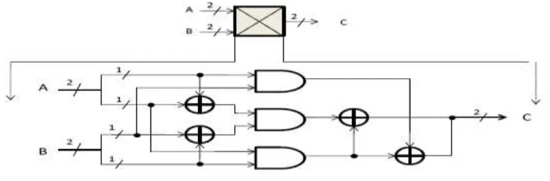
Sub bytes : The Sub Bytes operation is a nonlinear byte substitution. Each byte from the input state is replaced
by another byte according to the substitution box (called the S-box). The S-box is computed based on a
multiplicative inverse in the finite field GF (28) and a bitwise affine transformation.
In this module The implementation of the composite field S-BOX is accomplished using combinational logic
circuits rather than using pre-stored S-BOX values. S-BOX substitution starts by finding the multiplicative
inverse of the number in [7]
444 |
P a g e
Addition in GF (2^4):Addition of 2 elements in Galois Field can be translated to simple bitwise XOR
operation Addition of 2 elements in Galois Field can be translated to simple bitwise XOR operation.
GF (2^4) multiplier: Sub Bytes is a nonlinear transformation that uses 16 byte substitution tables (S-Boxes).
An S-Box is the multiplicative inverse of a Galois field GF (2^4) followed by an affine transformation.
Although two Galois Fields of the same order are isomorphic, the complexity of the field operations may
heavily depend on the representations of the field elements. Composite field arithmetic can be employed to
reduce the hardware complexity. Three multipliers in GF (24) are required as a part of finding the multiplicative
inverse in GF (2^8). Fig. shows the GF (2^4) multiplier circuit. As can be seen from the figure the GF (24)
multipliers consist of 3 GF (22) multipliers with 4 XOR Gates and with constant multiplier θ. This constant
multiplier which has 2 bits input extracts the lower bit output as the higher bit input, while the higher output bit
will be the result of XOR operation between the 2 input bits. Full derivation of this multiplier circuit can be
found[7].
Fig 2. GF (2
4) Multiplier
GF (2^2) Multiplier: While each finite field is itself not infinite, there are infinitely many different finite fields;
their number of elements (which is also called cardinality) is necessarily of the form pn where p is a prime
number and n is a positive integer.
Fig 3.Implimentation of the GF (2^2) multiplier
GF (2^4) squarer:It consists of bitwise xor operation. A bitwise operation operates on one or more bit
atterns or binary numerals at the level of their individual bits. It is a fast, primitive action directly supported by
445 |
P a g e
processors, typically, bitwise operations are substantially faster than division, several times faster than
multiplication, and sometimes significantly faster than addition. While modern high-performance processors
usually perform addition and multiplication as fast as bitwise operations, the latter may still be optimal for
overall power/performance due to lower resource use.
Fig 4.Hardware diagram for Squarer in GF (2
4)
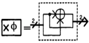
Constant multiplier (Xϕ):
Fig 5.Hardware implementation of multiplication with constant Φ
Constant multiplier (L):
Fig 6.Hardware diagram for multiplication with constant
446 |
P a g e
Fig 7. Implemented hardware architecture on the FPGA
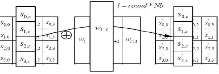
AddRoundKeyTransformation:
In the Add Round Key transformation, a round key is added to the state by Bitwise Exclusive-OR (XOR)
operation. Figure below illustrates the Add Round Key. This transformation is the same for both encryption and
decryption.
Shift Rows Transformation (Inv Shift Rows):
Shift Rows is a cyclic shift operation in each row of the State. In this operation, the bytes in the first row of the
state do not change. The second, third, and fourth rows shift cyclically to the left one byte, two bytes, three
bytes, respectively, as illustrated in Figure. The reverse process, inv Shift Row, operates in reverse order to Shift
447 |
P a g e
Mix Column Transformation (Inv Mix Column):
The Mix Column transformation is performed independently on the state Column-by-column. Each column is
considered as four term polynomial over GF (28) and multiplied by
a(x) modulo (x4 + 1) where a(x) = {03}x3 + {01}x2 + {01}x + {02}
This transformation can be expressed in matrix form as
Small Encryption:
The Small model implements an AES cipher on FPGA with the fewest processing Elements. As shown in
bellow Fig, it requires at least eight blocks to implement an AES cipher with online key expansion process,
since each Block on FPGA has only a 128 X 32-bit instruction memory and a 128 X 16-bit data memory[5].
III SIMULATION AND RESULTS
VHDL is used as the hardware description language because of the flexibility to exchange among environments.
448 |
P a g e
simulator. This is used for writing, debugging, simulating and checking the performance results using the
simulation tools available on Xilinx ISE. The delay is calculated with three different Device families [7].
Snapshot is nothing but every moment of the application while running. It gives the clear elaborated of
application. It will be useful for the new user to understand for the future steps.
3.1 VARIOUS SNAPSHOTS
Encryption top module
449 |
P a g e
Decryption
Block
RTL schematic
450 |
P a g e
Decryption:
IV CONCLUSION
The combination of a simple, portable and efficient AES cryptographic algorithm implemented in VHDL source
code provides an excellent platform for high security applications. A synthesizable VHDL code is developed for
the implementation of both encryption and decryption process. Each program is tested with Spartan 3 FPGA
device and output results are verified. Encryption and decryption routines are fully functional at 50 and 100
MHz The software generated key expansion was simulated and run on hardware without the keyboard input and
LCD output. Thus, AES can indeed be implemented with reasonable efficiency on an FPGA
.
REFERENCES
[1] National Inst. Of Standards and Technology, “Federal Information Processing Standard Publication 197, the Advanced Encryption Standard (AES),” Nov. 2001
[2] J. Daemen and V. Rijmen,” AES Proposal: Rijndael,” AES Algorithm Submission, Sept. 1999
[3] William Stallings, Cryptography and Network Security, Principles and Practices, 4th ed. Pearson Education,
pp. 134-161, 2006
[4] Charlie Kaufman, Radia Perlman, Mike Speciner, Network Security, Private Communication in a Public
World, 2nd ed. Pearson Education, pp. 41-114, 2006
[5] Wayne Wolf, “FPGA-Based System Design, Pearson Education, pp. 17-37
[6] Xinmiao Zhang and Keshab K. Parhi, “Implementation Approaches for the Advanced Encryption Standard
451 |
P a g e
[7] G. Rouvroy, F.-X. Standaert, F.-X.J.– J. Quisquater, J.-D. Legat, “Compact and Efficient
Encryption/Decryption Module for FPGA Implementation of the AES Rijndael Very Well Suited for Small
Embedded Applications,” Proc. ITCC-04 Conf., pp. 583-587, 2004
[8] Chih-Chung Lu and Shau-Yin Tseng, “Integrated Design of AES (Advanced Encryption Standard)