IJEDR1702154
International Journal of Engineering Development and Research (www.ijedr.org)922
Design and Implementation of FPGA based Logic in
Memory Multiprocessor Architecture for
Multi-Valued Data Transfer Schemes
1
Shaik Nazeer,
2N. Samba Murthy,
3Dr. M. Kamaraju
1PG Student, 2Asst.Prof, 3Prof.HOD 1Electronics And Communications Engineering, 1Gudlavalleru Engineering college, Gudlavalleru, India.
_____________________________________________________________________________________________
Abstract—Intensive computational architecture is to take on huge parallelism, with a lot of concurrent task’s to execute
simultaneously. This approach has many advantages, such as the reduced design time given by circuit replication and an increasing in computational speed without the need of higher frequency. Communication bottle neck between memory and logic module is one of the most serious problems in VLSI systems, So it is an important proof for bottle neck in data exchange between memory and logic module. To solve this, a new logic-in-memory VLSI architecture based on multi-valued data transfer is proposed to solve the communication bottleneck between memory and logic modules. Logic-in-Memory (LIM) architecture mixes logic and memory in the same device, removing the bottleneck of other existing parallel. By this we achieve power optimization under a time/area constraint, soft computing is investigated towards optimization of low power VLSI architecture design. So this logic-in-memory architecture to solve the data transfer bottlenecks.
_____________________________________________________________________________________________
I
INTRODUCTIONPresent days digital systems demand increasing electronic aid, so the multiprocessor are a suitable platform for them. This approach provides better results in term of area, speed and power consumption compared to a uni-processor systems. Reconfigurable multiprocessor systems are embedded system, implemented using reconfigurable hardware (FPGA).
Field Programmable Gate Array (FPGA) consists of ten thousand to more than a million logic gates with programmable interconnection. Programmable inter- connections are available for users to perform given functions easily. There are I/O blocks, which are designed and numbered according to function. For each module of logic level composition, there are CLB’s (Configurable Logic Blocks). CLB performs the logic operation given to the module. The inter connection between CLB and I/O blocks are made with the help of horizontal routing channels, vertical routing channels, PSM and Programmable Multiplexers.
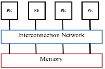
Fig 1. Architecture of VLSI Processor
© 2017 IJEDR | Volume 5, Issue 2 | ISSN: 2321-9939
IJEDR1702154
International Journal of Engineering Development and Research (www.ijedr.org)923
concept was introduced [1].In this Processor Element (PE), Interconnection Network and Memory are present. PE is presented and designed by a VHDL structural modeling and it consists of registers for storage purposes and flags and logic systems. This unit will be used in an implementation of a multiprocessor system on one FPGA chip (SoC).
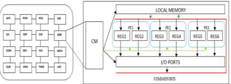
Fig 2. Shared Memory Multi Processor
Shared memory multi processor is showed in the above figure.Fig.2. In this each PE has its private memory, so one PE cannot read directly to another PE. Data transfer was performed by using message passing protocol. With this approach the delay problem will not rectified but reduced to some extent when compared to VLSI processor. To overcome the above constraints introduced the Logic-In-Memory concept in this paper. In a Logic-In-Memory structure the storage function are allotted over a logic circuit plane.. The data which is stored in the storage device will be included in each cell of LIM VLSI array, its VLSI array may be regarded either as a logically enhanced memory array, or as a logic array whose elementary gates and connections can be programmed to realize a desired logical behavior.
In this paper Logic-In-Memory Multi Processor architecture is proposed which has higher speed and lesser delay and area. The paper structured as follows Section II explains the Proposed Logic-In-Memory Multi Processor architecture for Multi Valued Data Transfer Schemes, Section III Explains Experimental Results, Section IV Conclusion.
II PROPOSED LOGIC-IN-MEMORY MULTI PROCESSOR ARCHITUCTURE
Before going to the LIM multi processor, we will discuss about LIM processor. The Fig.3 shows the LIM processor, in this left block is the memory block and the right block is the processor.
In the memory block the LIM cells are present which are inter connected to each cell. In the every cell the preferred logic is embedded and the processor will directly execute the preferred logic form the memory cell with any delay.
Fig.3 Logic-In-Memory Processor
Coming to the processor, the processor has Configuration Memory (CM),local Memory(LM), Registers, ALU and common bus to perform read, Write operation. The preferred logic is selected to execute the CM will get the total information about the logic which has to be performed, from there it store the information in the local memory. The local memory will pass the inputs to the registers and the registers will pass the information to the ALU unit to execute the operation. And the total operation from Local memory to the ALU unit is carried out through the common bus. The main specialty of the common bus is, to perform the read, write operation in a single clock cycle.
IJEDR1702154
International Journal of Engineering Development and Research (www.ijedr.org)924
Fig.4 Logic In Memory Multi Processor
Although the LIM processor and the LIM multi processor has memory block, and processor block. Fig 4 shows the memory block in LIM cells and directly embedded with binary instructions. The function of each instruction is described in the below table.1.After storing the logic in the memory cell they execute in the form of concurrent computing.(one completing before the next starts).
Table I. Instructions
opcode Binary code operation
LXN 1111101010 The contents of a and b are EX-ORed and the result will be
stored in a.
ROR 1111111111 The content of a reg is rotated right through carry by 1bit. ROL 1111111110 The content of a reg is rotated left through carry by 1bit.
LSR 1111111100 The content of a reg is shifted right by 1 bit.
LSL 1111111000 The content of a reg is shifted left by 1 bit.
SER 1111110000 All the bits of a red are set to logic 1.
CLR 1111100000 All the bits of a reg are cleared.
COM 1111000000 The content of a and b reg are compared.
© 2017 IJEDR | Volume 5, Issue 2 | ISSN: 2321-9939
IJEDR1702154
International Journal of Engineering Development and Research (www.ijedr.org)925
INC 1100000000 The content of reg is incremented by 1.
MOV 1000000000 The content of a reg is moved to b reg.
ADD 0000000001 The content of a and b reg is added and results will be in a.
SUB 0000000010 The content of a and b reg is subtracted results will be in a.
ONE 0000000011 The content of reg is 1’s complimented and results will be in a.
TWO 0000000100 The content of reg is 2’s complimented and results will be in a
LAD 0000000101 The content of a and b ANDed and results will be stored in a.
LOR 0000000110 The content of a and b ORed and results will be stored in a.
LNA 0000000111 The content of a and b EX-ORed and results will be stored in a.
SWP 1111111010 The content of a and b reg’s are swapped.
The Processor Element(PE) consists of registers, processing unit, control unit, accumulator, flags and these are briefly explained in[3].In the LIM multi processor, three processor elements are present and they perform according to the instruction in SIMD, MIMD, SISD, MISD[3].The operation of the LIM multi processor is same as the LIM processor, due to the number of processor elements increases the processor has fast execution and no waiting period occurs. So, the drawback of LIM processor is rectified in the LIM multi processor.
IJEDR1702154
International Journal of Engineering Development and Research (www.ijedr.org)926
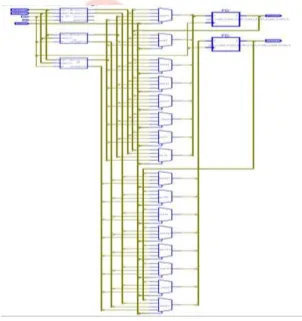
Fig.5. RTL Schematic Diagram of Proposed ArchitectureFig.6. Internal RTL Schematic Diagram of Proposed Architecture.
RTL diagram represents the schematic of embedded multiprocessor core. The embedded multiprocessor
schematic represents the Multi bus organization, multiple Alu’s, multiple I/O ports with their internal connections are
shown in Fig.6 .
U0: Signals description of Databus1
© 2017 IJEDR | Volume 5, Issue 2 | ISSN: 2321-9939
IJEDR1702154
International Journal of Engineering Development and Research (www.ijedr.org)927
Input : data1(7:0) => operand1(7:0)Input : data2(7:0) => operand2(7:0) Output : out1(7:0) => A(7:0)
Output : out2(7:0) => B(7:0)
Input : rs => ALE (It is same input signal for All data bus modules )
Input : sel(1:0) => PS1(1:0)
U1: Signals description of Databus2
Bidirectional : addr3(15:0) => addr3(15:0)
Bidirectional : addr3(15:0) => addr3(15:0)
Bidirectional : addr3(15:0) => addr3(15:0)
Input : data3(7:0) => operand3(7:0)
Input : data4(7:0) => operand4(7:0)
Output : out3(7:0) => C(7:0)
Output : out4(7:0) => D(7:0)
Input : sel1(1:0) => ps2(1:0)
U2: Signals description of Databus3
Bidirectional : addr5(15:0) => addr5(15:0) Bidirectional : addr6(15:0) => addr6(15:0) Input : clk => clk
Input : data5(7:0) => operand5(7:0) Input : data6(7:0) => operand6(7:0) Output : out5(7:0) => E(7:0) Output : out6(7:0) => F(7:0)
Input : sel3(1:0) => ps3(1:0)
U3: Signals description of Alu1
Input : a(7:0) => A(7:0) Input : b(7:0) => B(7:0) Input : clka => clk Output : op(7:0) => op(7:0) Input : operation(1)(7:0) Input : operation (2)(7:0) Input : operation(3)(7:0) Output : op1(7:0) => op1(7:0
U4: Signals description of Alu2
IJEDR1702154
International Journal of Engineering Development and Research (www.ijedr.org)928
Input : clka => clkInput : operation(1)(7:0) Input : operation(2)(7:0) Input : operation(3)(7:0) Output : op11(7:0) => op11(7:0) Output : op21(7:0) => op21(7:0)
U5:Signals description of Alu3
Input : a3(7:0) => E(7:0) Input : b3(7:0) => F(7:0) Input : clka => clk Input : operation(1)(7:0) Input : operation(2)(7:0) Input : operation(3)(7:0) Output : op13(7:0) Output : op31(7:0)
Fig. 7 RTL Schematic of Multi Data bus module
In the multi data bus each data bus is shared to individual processors and it is depends on the data selected by different ports through muxes are shown in fig.7.
III. EXPERIMENTAL RESULTS
© 2017 IJEDR | Volume 5, Issue 2 | ISSN: 2321-9939
IJEDR1702154
International Journal of Engineering Development and Research (www.ijedr.org)929
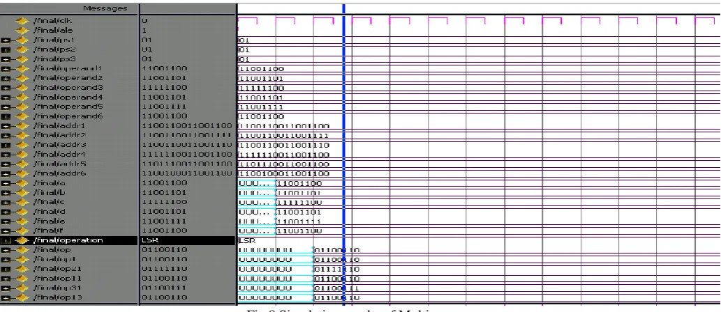
Fig 8 Simulation results of Multi processor
Simulation results of multi processor are shown in fig.8 and 9. In this “LSR” instruction is executes through multiple data of different processor1, 2 and 3 operates on the designed multiprocessor core which shows the parallel computing. Before computation the data will be loaded in to the Duplicate memories of operand1, operand2, operand3, operand4, operand5, operand6.which is more competent for the designed concurrent architecture.
Fig 9 Simulation results of Multi processor
Here the instruction performed is the ADD operation, to get the desired output the following information is given as the input data OP1=11001101 , OP=11001101 and the output obtained is the OP=10011010. Clk, rs, sel, input signals and data1 data2 ,addr1,addr2 are the output signals. The addition operation was performed by forcing the string as “ADD”.
Table II. Comparison of Architectures
Parameters Existing work Proposed work
Number of slices LUTs 987 694
Number of 4 input LUTs 1678 1279
Number of bonded IOBs 342 272
Time Delay 5.92ns 4.674ns
IJEDR1702154
International Journal of Engineering Development and Research (www.ijedr.org)930
The designed Logic-In-Memory Multi-processor architecture is implemented using verilog coding and verified synthesis results using Xilinx ISE software. The designed system reduces the no of LUT’s and I/O blocks compared to existed system and the clock speed of the designed system is 4.674ns.In future conducting further investigation that integrate a software system using FPGA hardware system.V.ACKNOWLEDGMENT
I heartily thank full to my institution and my faculty for their support , and my friends for helping me in work.
REFFERENCES
[1] Mohamed EL KHAILI ,“Multiprocessor Architecture Design Using VHDL Structural Modelling”, IRACST – Engineering Science and Technology: An International Journal (ESTIJ), ISSN: 2250-3498 Vol. 5, No. 2, April 2015.
[2]. Brown S., Vranesic Z “Fundamental of Digital Logic Design with VHDL” McGraw Hill, 2nd Edition.
[3]. D. Göhringer, T. Perschke, M. Hübner and J. Becker , “A taxonomy of reconfigurable single/multiprocessor Systems-on-Chip » International Journal of Reconfigurable Computing, Article ID 570279, vol. 2009, 11 pages, 2009.
[4]. Xiao, Zhengyu He and Bo Hong, “An Analytical Model on the Execution of Transactional Memory”, 22nd International Symposium on Computer Architecture and High Performance Computing (SBAC-PAD 2010), October (2010).
[5]. BoHong & ZhengyuHe,“An Asynchronous Multi-threaded Algorithm for the Maximum Network Flow Problem with Non- blocking Global Relabeling Heuristic”, IEEE Transactions on Parallel and Distributed Systems, 22(6): 1025-1033, (2011). [6]. j. Daniel, V. Taliwal, A. Meier, W. Holfelder, and R. Herrtwich, “design of 5.9 ghz dsrc-based vehicular safety
communication,”ieee wireless commun. Mag., Vol. 13, no. 5, pp. 36–43, oct. 2006
[7]. Tai-Hua Lu, Chung-Ho Chen and KuenJong Lee, “Effective Hybrid Test Program Development for Software-Based Self-Testing of Pipeline Processor Cores” IEEE Manuscript received April 03, 2009, revised August 14, 2009, first published December 18, (2009).
[8]. Y.-C. Hung, M.-M. Kuo, C.-K. Tung, and S.-H. Shieh, “High-speed CMOS chip design for Manchester and Miller encoder,” in Proc. Intell. Inf. Hiding Multimedia Signal Process., Sep. 2009, pp. 538–541.
[9]. M. A. Khan, M. Sharma, and P. R. Brahmanandha, “FSM based Manchester encoder for UHF RFID tag emulator,” in Proc. Int. Conf.Comput., Commun. Netw., Dec. 2008, pp. 1–6.
[10]. M. A. Khan, M. Sharma, and P. R. Brahmanandha, “FSM based FM0and Miller encoder for UHF RFID tag emulator,” in Proc. IEEE Adv.Comput. Conf., Mar. 2009, pp. 1317–1322.
[11]. J.-H. Deng, F.-C. Hsiao, and Y.-H. Lin, “Top down design of joint MODEM and CODEC detection schemes for DSRC coded-FSK systems over high mobility fading channels,” in Proc. Adv. Communs. Technol. Jan. 2013, pp. 98–103. [12]. Sumedh .S.Jadhav, “FPGA Based Embedded Multiprocessor Architecture“ International Journal of Electrical and