IJIRT 147985
INTERNATIONAL JOURNAL OF INNOVATIVE RESEARCH IN TECHNOLOGY724
Formation of Intermetallic Compounds in Diffusion
Soldering Joints in High Temperature Power Electronic
Applications
C. Chaki
1, M. Chaki
2, and K. Roy
3 1M.Sc., Friedrich-Alexander-Universität Erlangen-Nürnberg, Germany
2B.Sc., Bangladesh University of Textiles, Dhaka, Bangladesh
3Assistant Professor, Rajshahi University of Engineering & Technology, Rajshahi, Bangladesh
Abstract-For any type of metal-based interconnections, intermetallic compounds (IMC) are needed to ensure the contact between different electronic chip layers. The connection between solder and direct copper bonded (DCB) is only possible through the intermetallic compounds (IMCs) such as Cu6Sn5 and Cu3Sn in Cu-Sn soldering system in diffusion soldering process. The IMCs are brittle in nature compared to the metals like tin (Sn) or copper (Cu). Due to the thermo-mechanical loading in service of the product, these brittle IMCs shows cracks/defects and eventually lead failure. But the optimized temperature profile provides the better mechanical and thermal stability of IMCs. In standard electronics, only thin layers of IMCs are realized as good solder connections because thick growth of IMCs leads to faster crack propagation in layer and failure of electrical connection. On the other hand, for high-temperature applications (e.g. power electronics), to avoid the problems with low-melting Sn-Cu based solders, one reliable solution is to transform the solder layer (Sn) between the chip and substrate (e.g. direct copper bonded (DCB)) is to be transformed into IMCs as they have better mechanical properties as well as thermal stability. But in practice the complete transformation of solder layer into IMCs take more time. It also depends on the dimension of solder (Sn) and substrate (Cu) material. If Sn thickness is so thin, formation of IMCs take less time because the diffusion is faster. When the thickness of Sn increases, the formation of IMCs take more time. An overview of IMCs formation in tin based Sn-Cu Transient liquid phase (TLP) soldering joints have been studied in this article and discussed its importance in Power Electronic applications as a reliable interconnection technology.
Index Terms- Diffusion soldering, IMC Formation,
Intermetallic Compound, Interconnection technology, Power Electronic applications.
I. INTRODUCTION
Power electronic devices as its technical
implementation specialize on the efficient
transformation of electrical energy as well as the management of the power flow. Due to the expected future economic and technological advancement, it is obvious that chip interconnections with high strength and resistance against thermo-mechanical stresses in combination with excellent thermal and electrical properties and low failure probabilities are needed. During soldering process in electronics production, interfacial interactions between a molten solder and a solid substrate result in the formation and growth of complex intermetallic compounds (IMCs) at the substrate and solder interface. Initially, the substrate partially dissolves into the molten solder alloy upon contact. The IMC layers continuously evolve during further solid-state aging at temperatures below the
melting point of the solder. Computational
simulations of IMCs growth and interface
IJIRT 147985
INTERNATIONAL JOURNAL OF INNOVATIVE RESEARCH IN TECHNOLOGY725
product, these brittle IMCs show cracks/defects andleads to failure.
II. DIFFERENT SOLDERING PROCESS
A. Standard Soldering
In today’s electronic production, lead-free soft solders are used due to ecological and health-related reasons. Since today’s technical applications demand an increase in power density, a clear trend for higher junction temperatures towards 175°C or even 200°C can be seen. This increase in junction temperature apparently contradicts the use of standard Sn based soft solders with melting points near 220°C. Operating such a soft solder joint at a homologous temperature Thom > 0.9 (with the homologous temperature Thom = Toperation / Tmelting will lead to an immediate failure of the joint under thermo-mechanical loading.
B. Diffusion Soldering (TLPB)
Transient liquid phase bonding (TLPB) describes a bonding technology based on a metal interlayer, which is melted and solid-solid as well as liquid-solid diffusion in the substrate material is stimulated. This is also the main difference to common diffusion bonding where only solid-state diffusion occurs. The main advantage of TLPB is the high melting point of the interconnection which lies above the bonding temperature, by contrast to regular soldering. In TLP bonding the solder, most of the time the higher melting component is provided by the substrate material (e.g. copper). Interlayer and substrate remain solid since no energy input occurred. The first acts of diffusion begin right when the substrate is first heated. Depending on inter-diffusion coefficients of interlayer and substrate as well as temperature-gradients a certain amount of interlayer molecules diffuse into the substrate. When the melting temperature of the interlayer is reached the formation of liquid bonding material starts. The set-up is then further heated up to the specific bonding temperature to ensure the complete melting of the interlayer metals and even further diffusion.
C. Diffusion Soldering (TLPS)
The TLPS process presents itself rather similar to the TLPB process, with the main difference that normal (lead-free) solder paste is used as interlayer material
and reaction partner for the intermetallic alloy formation. Depending on the choice of chip metallization and the soft solder material in standard soldering usually Cu-Sn or Ni-Sn IMCs are formed as thin interfacial layers. All these IMCs have a much higher melting point than the Sn-based soft solders. For example, depending on the process parameters in the Cu-Sn system either Cu3Sn with Tm=676°C or Cu6Sn5 with Tm=415°C is formed during the soldering process. [2], [3]
While TLPS and standard both joints are formed from a Sn-rich solder, in the standard joint only a fraction of the Sn is transferred into a high melting intermetallic. By contrast, in the diffusion soldered joint, the whole volume of low melting solder is consumed by the solidification process. The result is a high melting bond between chip and substrate. Depending on the ratio between the two different intermetallic phases, that are formed in the Cu-Sn system, the homologous temperature for these joints ranges from Thom=0.52 – 0.65. [4]
Transient liquid phase soldering combines high junction temperatures (up to 676°C for Cu3Sn) with a relatively simple process that can theoretically be performed in any reflow furnace. The deciding advantage of TLPS is that standard lead-free SnCu solder paste can be used as interconnecting base material, by contrast to special foils or metallization in the TLPB process. [5], [6]
III. IMC GROWTH IN DIFFUSION SOLDERING
During the solid-liquid-solid interaction of molten solder and Cu substrates, it is believed that rapid dissolution of Cu into molten solder with a lower Cu concentration occurs immediately after the Cu oxide film has been removed by the actions of the flux. This rapid direct dissolution of Cu occurs until the conditions become favorable for the nucleation and growth of IMCs such as Cu6Sn5 and Cu3Sn. [7] The rapid dissolution of Cu into molten solder is important in understanding the evolution of IMC formation particularly during the soldering process, as the size and morphology of IMCs have been associated with joint reliability. [8], [9]
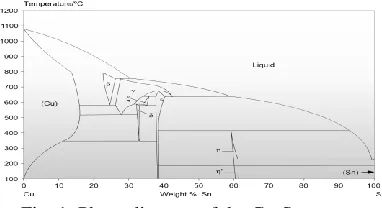
A. Phase Diagram of Cu-Sn System
IJIRT 147985
INTERNATIONAL JOURNAL OF INNOVATIVE RESEARCH IN TECHNOLOGY726
crystal structure. IMCs (Cu6Sn5, Cu3Sn) aregenerally brittle in nature and have a high melting point. As seen in Fig. 1, the relevant phases to look at in the Cu-Sn system are Cu6Sn5 and Cu3Sn, which form from molten Sn-solder in a realistic temperature field (under 350°C).
Fig. 1: Phase diagram of the Cu-Sn system Figure 1 also shows that Cu6Sn5 exists in two different forms: The stable η’ and the metastable
high-temperature η. Since the transformation
temperature of Cu6Sn5 is 186°C the formation of η’ should only occur in high-temperature applications (regular use above 150°C). Cu3Sn (ε-phase here) has a higher Cu-Sn ratio and therefor also a higher melting point (676°C). [10]
A. Intermetallic Phase Formation
The diffusion of Cu into liquid solder results in the nucleation of IMCs in the bulk of the solder material which leading to: (a) super-saturation of the Cu in Sn-based alloy caused by cooling, and (b) consumption of the Sn by interfacial IMC formation, resulting in an increase of the degree of super-saturation of Cu in the Sn-based alloy. It has been observed that the growth rate of IMC precipitates during reflow is initially very fast as a result of super-saturation. In other words, the local concentrations of Cu dissolved in the molten Sn, decrease as IMC islands are formed. As any solid liquid bonding technique, Cu/Sn bonding is based on rapid formation of IMCs between two metal components: one low-melting component (Sn) and one high melting component (Cu). The bonding is typically carried out at moderate temperatures between 250°C and 300°C which is above the melting point of Sn. When the Sn melts, the IMCs solidify isothermally. For correctly designed layer thicknesses, the resulting bond-line will only consist of Cu and the intermetallic phases (Cu6Sn5 and Cu3Sn), with
melting temperatures of 415°C and 676°C
respectively.
Fig. 2: (a) Cross-sectional image of the formation of intermetallic phase Cu-Sn system under isothermal
aging (b) Movement of intermetallic compound in Cu-Sn interconnection [11], [12]
For the typical temperature gradients in a TLP – process, the Cu6Sn5 phase is the first one to form. Firstly, the substrate's Cu is dissolved in the liquid Sn solder until the liquid interlayer is supersaturated. This happens in the first few seconds of the process and is also the reason why the first Cu6Sn5 crystals can be observed this fast. The resulting structure must be divided in the scallop type phase which forms right on the edges of the Copper substrate and the two phase (Cu6Sn5 + Sn) structures on top of it. [13] The growth mechanisms of those structures are relatively hard to predict. Common opinions suggest that they are mainly influenced by local differences in dissolution on the Cu-surface. This inequalities lead to parts in the layer with relatively large amounts of free copper atoms, which are then used to form Cu6Sn5 scallops in the primary structures as well as Cu6Sn5 scallops in the two-phase middle part of the interlayer. Better circumstances for the Cu3Sn growth are reached after solidification of the bond, due to its strong dependence on a long contact time. Considering the details in reaction kinetics occurring at varying temperatures, thicknesses or materials, contradictory results have to be recognized. While it is well known that a long contact time as well as high-temperature have a positive effect on the diffusion mechanisms that lead to the phase
formation, differing approaches towards a
scientifically exact reaction model in the Cu-Sn system and in general have been performed. [14]
Fig. 3: Intermetallic formation in diffusion soldering process; (i) Solder paste on substrate, (ii) Conventional solder connection, (iii) Diffusion
IJIRT 147985
INTERNATIONAL JOURNAL OF INNOVATIVE RESEARCH IN TECHNOLOGY727
In Fig. 3, the Intermetallic formation in diffusionsoldering process where solder paste on substrate, Conventional solder connection and diffusion soldered joint are presented.
IV. IMPROTANCE OF INTERMETALLICS
Intermetallic compounds play an increasingly critical role to the performance and reliability of solder interconnections in the chip level, package level and board level of lead-free electronics. The intermetallic compounds are an indication of chemical bonding at the substrate/solder interface. So certain amounts of intermetallic formation can be considered to indicate that the soldering process has formed a good bond. Intermetallic compounds produce improvements in the mechanical and thermal properties of solder joints, and promote wetting and bonding processes. Their hardness is usually several times greater than that of the tin, and their conductivity is usually better than that of the tin. The intermetallic phases are products of the solder-substrate interactions. An initial layer forms during the soldering process, and continues to grow in the solid state, especially at elevated temperatures. [16], [17] The combination of the Cu3Sn and Cu6Sn5 layers seems to result in a very strong bond between the solder and the copper. [18]
Fig. 4: Cross-section of a power electronic module [19]
In all the soldering processes of electronics assembly, an IMC formation is the basic and crucial starting point for bond formation. A conventional soldering process starts with the formation of intermetallic between solder layer and base substrate and the IMC grows in thickness with time through subsequent reflows and aging. Two commonly known properties in all IMCs are the hardness and brittle nature. The latter property however can cause joint embrittlement leading to failure of the device during thermo- mechanical loading. Depending on the morphology and distribution of the phases, small amounts can produce distinct improvements in mechanical and thermal properties.
Transient liquid phase soldering (TLPS) has the combining features of conventional soldering and diffusion bonding process. The advantage is it forms the phases with very high melting points and mechanical strength. The bonded joints from standard Sn-based soft solders do not melt unless the assembly is heated up to the melting point of the formed phases i.e., 415°C for Cu6Sn5 and 676°C for Cu3Sn. However the process necessary to form these phases needs relatively long handling times, incompatible with normal production processes. One important application of this diffusion soldering technology is chip-substrate interconnect in power electronics where the operating temperatures can exceed the joining process temperatures leading to failure of the
device. Though the new generation power
semiconductor chips are capable of sustaining high temperatures for longer periods, the failure issue raises in the reliability of the packaging technology. As explained, the overall lifetime of a power module varies with the implementation of improved technology, reducing the degradation effects on wire bonds on the chip top side and improving thermal management from the chip bottom side. [20]
V. VOID FORMATION
IJIRT 147985
INTERNATIONAL JOURNAL OF INNOVATIVE RESEARCH IN TECHNOLOGY728
The formation of Kirkendall voids results fromunbalanced diffusion of copper and tin atoms in solid-state-reactions between copper-substrate and Sn-Cu solder. This effect is observed in lead-free as well as in tin-lead solder. During isothermal aging the Cu3Sn intermetallic phase grows at the expense of the Cu6Sn5 phase as illustrated in below reactions. The initial Cu3Sn growth reaction can be formulated as:
Cu6Sn5 = 2Cu3Sn + 3Sn Sn + 3Cu = Cu3Sn
There are two possibilities for the copper to diffuse for IMC formation. Firstly it can originate from the DCB / IMC interface and secondly it could diffuse from existing Cu3Sn phase directly into the Cu6Sn5 scallops. Studies have shown that the latter mechanism is much faster than the direct solution of copper out of the pure form, and this way also the process that happens predominately in reality. This rapid diffusion movement leaves vacancies of atomic size where the copper was extracted. These holes also cannot be filled with residual Sn-atoms. The result is a condensation of these vacancies and the formation of the so-called Kirkendall voids. Kirkendall voids have become a widely feared failure mode, leading to cracks and faster thermal degradation of the bond region. [24], [25]
VI. THEORITICAL CALCULATION OF IMC THICKNESS
The IMC growth at a solder/Cu interface can be adequately modeled with the empirical power law as the following equation
Where X is the thickness of interfacial IMC or the Sn thickness that has reacted with Cu to form IMCs after the annealing time duration t (reaction time), D is growth rate constant which is equivalent to diffusivity if IMCs formation is diffusion controlled and n is the time exponent. In general, the solid state growth can follow either linear or parabolic
growth kinetics. When n=1, the interfacial IMC
growth follows the linear law which implies the growth rate is limited by the reaction rate at growth site. [26] When n= 1/3, the interfacial IMC growth follows the parabolic law and is grain boundary diffusion-controlled. When n= 1/2, the interfacial
IMC growth follows the parabolic law and is volume diffusion controlled. In contrast, parabolic growth indicates that the growth is controlled by atomic diffusion. Most of researches use a comprehensive diffusivity parameter for the whole IMCs layer formed at the bond interface due to the complexity to distinguish individual IMC phase and measure its thickness as they are usually non-homogenously layered against each other. [27], [12] The diffusion coefficient is a function of temperature which is expressed by Arrhenius equation which is expressed below. [28]
(
)
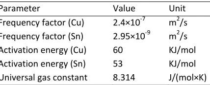
Where Do is a temperature-independent constant known as the frequency factor, Q is the activation energy for diffusion, R is the universal gas constant, and T is the absolute temperature in degrees Kelvin. By measuring the individual intermetallic thickness at various temperatures, the activation energy and diffusion coefficient of each phase can be acquired. It must be noted that intermetallic growth rate can vary depending on the bonding materials and conditions. The inter-diffusion can be more rapid if there are more defects such as vacancies, dislocations and grain boundaries. Thus, the obtained activation energies and diffusion coefficients can vary and be very much microstructure dependent. Theoretically the above equation is used to calculate the diffusivity of individual intermetallic phase based on the experimental data of activation energy and diffusion coefficient.
Table 1: Material characteristics of Cu and Sn
Parameter Value Unit
Frequency factor (Cu) 2.4×10⁻⁷ m2/s Frequency factor (Sn) 2.95×10⁻⁹ m2/s Activation energy (Cu) 60 KJ/mol Activation energy (Sn) 53 KJ/mol Universal gas constant 8.314 J/(mol×K)
VII. EXPERIMENTAL RESULTS
A. Experimental material
For the evaluation of interconnections and the formation of IMCs, pure Cu and Sn with dimension of 5x5 mm were taken. The thickness of both pure materials (Cu and Sn) were chosen as 40 µm. For the
IJIRT 147985
INTERNATIONAL JOURNAL OF INNOVATIVE RESEARCH IN TECHNOLOGY729
considered. Vacuum Vapor Phase soldering machinewas taken for the experimentation. The dimension of the experimental setup is shown in below.
Fig. 5: Cross section of Cu and Sn with dimensions B. Experimental case
Three particular cases were experimented for this study. In case 1, Cu-Sn system was heated from room temperature (25°C) to a peak temperature (TP=260°C and 280°C) with a heating rate (H∆=2.5 °C /s). Then it was further heated at a constant peak temperature for some time which is called holding time at TP. Thereafter, the system was cooled down to the room temperature again with a constant cooling rate (C∆=2.5 °C/s). For case 2, with constant heating rate (H∆=2.5 °C/s) at TP =260°C, the cooling rate and holding time at peak temperature was varied. By varying C∆ from 1 °C/s to 3 °C/s and holding time at TP =260°C from 1.5 min to 20 min, different IMC thickness was observed which is presented in table 3. For the case 3, Cu-Sn system was heated in a same way from room temperature (25°C) to the peak temperature (TP=260°C) with same H∆. It was then heated constantly at Tp for some time and pre-cooled with a constant cooling rate (C∆=2.5 °C/s) until an intermediate temperature (Tinter=210°C). After holding some time at Tinter it was cooled down to the room temperature with a constant cooling rate (C∆ =2.5 °C/s). The experimental results are presented in table 2, 3 and 4 respectively.
C. Experimental Results
Table 2: IMC thickness at TP= 260°C and 280°C
H∆
(°C/s) Time (min)
C∆
(°C/s)
IMC Thickness (µm) TP = 260°C TP = 280°C
Cu6Sn5 Cu3Sn Cu6Sn5 Cu3Sn
2.5 1.5 2.5 2.5 0.3 2.5 0.3
2.5 5 2.5 3 0.5 3.2 0.8
2.5 10 2.5 3 0.8 4.3 1
2.5 15 2.5 6.8 0.9 7.1 1
2.5 20 2.5 7.1 1 9.3 1.1
2.5 25 2.5 10.5 1 12.3 1.6
2.5 30 2.5 12.1 1.5 13.7 1.9
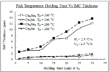
The maximum IMC thickness for Cu6Sn5 and Cu3Sn is observed at peak temperature of TP=280°C with long soldering time. It is clear that high TP and longer soldering time has positive impact on IMC thickness.
Fig. 6: IMC thickness at TP=260°C and 280°C The formation of the Cu6Sn5 structures created on Cu interfaces as scallop-type shape in the beginning of the soldering process. In later periods of the IMC growth process, the grain growth then depends strongly on peak temperature (TP) and total soldering time [29]. As illustrated in Fig. 7, high soldering temperature generally leads to larger diameters of forming Cu6Sn5 scallops which can produce elongation of the existing scallop type particles, leading to prism-type or hexagonal-type structures, which elongate in the direction of their growing axis along with the soldering process. [30], [31], [32]
IJIRT 147985
INTERNATIONAL JOURNAL OF INNOVATIVE RESEARCH IN TECHNOLOGY730
In case 2, it has been observed that the combinationof slow cooling rate and longer soldering time has positive impact on IMC thickness which is illustrated in table 3.
Table 3: IMC thickness at TP=260°C with varying cooling rate (C∆) and holding time at TP
TP =260°C IMC Thickness (µm)
H∆
(°C/s) Time (min)
C∆
(°C/s) Cu6Sn5 Cu3Sn
2.5 1.5 1 2.3 0.5
2.5 1.5 2 2 0.3
2.5 1.5 2.5 2.5 0.3
2.5 10 2.5 3 0.8
2.5 20 1 8.5 2.1
2.5 20 3 7.1 1
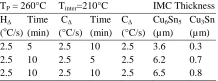
In case 3, the maximum IMC thickness for both Cu6Sn5 and Cu3Sn are recorded while increasing the
soldering time with constant H∆ and C∆ at TP and Tinter
Table 4: IMC thickness at TP=260°C and
Tinter=210°C with varying cooling rate (C∆) and
soldering time
TP = 260°C Tinter=210°C IMC Thickness
H∆
(oC/s) Time (min)
C∆
(°C/s) Time (min)
C∆
(°C/s)
Cu6Sn5
(µm)
Cu3Sn
(µm)
2.5 5 2.5 10 2.5 3.6 0.3
2.5 10 2.5 5 2.5 6.2 0.7
2.5 10 2.5 10 2.5 6.5 0.8
VIII. MODELING AND SIMULATION
For the fast growing electronics manufacturing industries, the growth kinetics of the interfacial IMCs for different solders/substrates combinations by experiments are not affordable. However modeling and simulation provides the basic understanding and an effective tool to measure the behavior of growth kinetics of IMC in solder materials during diffusion
soldering. Modification of materials, process
parameters, boundary conditions, varying mechanical pressure and changing the soldering temperature & time are much easier, less time consuming and cost effective in computer based simulation approach rather than physical experimentation while generating and comparing results. In the next article a simplistic mathematical model will be developed to simulate IMCs growth kinetics using numerical method and
compare with the experimental results to validate the developed model.
IX. CONCLUSION
The largest challenge of diffusion soldering is the controlled reduction of voids, especially in high temperature soldering profiles which are required for strong IMC growth in the interlayer. Better performances is observed for high peak temperature and longer soldering time with a constant heating and cooling rate. For a solder (Sn) and substrate (Cu) height of 40µm a maximum thickness of Cu6Sn5 and Cu3Sn was obtained by 13.7 µm and 1.9 µm respectively with the experimental variable of TP=280°C, H∆=C∆=2.5 °C/s and total soldering time 33.4 minutes. A void free solder joint with completely transformed IMCs can be obtained with 280°C solder profile, appropriate thermal treatment and longer soldering time therefore extraordinary high- temperature strength would be guaranteed. A comprehensive simulation technique would be applied in the next article to simulate the growth rate of IMCs and validated with the experimental outcomes.
REFERENCES
[1] M. S. Park and R. Arróyave, “Computational
investigation of intermetallic compounds
(Cu6Sn5 and Cu3Sn) growth during solid-state aging process,” Comput. Mater. Sci., vol. 50, no. 5, pp. 1692–1700, 2011.
[2] C. Buttay, D. Planson, B. Allard, et al., “State of the art of High Temperature Power Electronics To cite this version : HAL Id : hal-00413349 State of the art of High Temperature Power Electronics,” 2009.
[3] K. Guth, D. Siepe, J. Görlich, et al., “New assembly and interconnects beyond sintering methods,” Infineon Technol. AG Editor. - PCIM Eur. 2010.
[4] G. Humpston, D. M. Jacobson, and S. P. S. Sangha, “Diffusion soldering for electronics manufacturing,” Endeavour, vol. 18, no. 2, pp. 55–60, 1994.
IJIRT 147985
INTERNATIONAL JOURNAL OF INNOVATIVE RESEARCH IN TECHNOLOGY731
Manuf. Technol., vol. 1, no. 4, pp. 457–478,2011.
[6] G. Bai, “Low-Temperature Sintering of
Nanoscale Silver Paste for Semiconductor Device Interconnection,” Virginia Polytechnic Institute and State University, 2005.
[7] L. Wang, Y. Wang, P. Prangnell, and J. Robson,
“Modeling of Intermetallic Compounds Growth Between Dissimilar Metals,” Metall. Mater. Trans. A Phys. Metall. Mater. Sci., vol. 46, no. 9, pp. 4106–4114, 2015.
[8] M. A. A. Mohd Salleh, S. D. McDonald, H. Yasuda, A. Sugiyama, and K. Nogita, “Rapid Cu6Sn5 growth at liquid Sn/solid Cu interfaces,” Scr. Mater., vol. 100, pp. 17–20, 2015.
[9] L. M. Lee and A. A. Mohamad, “Interfacial reaction of Sn-Ag-Cu lead-free solder alloy on Cu: A review,” Adv. Mater. Sci. Eng., vol. 2013, 2013.
[10]F. Lang, H. Yamaguchi, H. Nakagawa, and H.
Sato, “High temperature resistant joint
technology for SiC power devices using transient liquid phase sintering process,” ICEPT-HDP 2012 Proc. - 2012 13th Int. Conf. Electron. Packag. Technol. High Density Packag., pp. 157–161, 2012.
[11]N. Zhao, Y. Zhong, M. L. Huang, H. T. Ma, and
W. Dong, “Growth kinetics of Cu6Sn5 intermetallic compound at liquid-solid interfaces in Cu/Sn/Cu interconnects under temperature gradient,” Sci. Rep., vol. 5, no. February, pp. 1– 12, 2015.
[12]T. T. Luu, A. Duan, K. E. Aasmundtveit, and N.
Hoivik, “Optimized Cu-Sn wafer-level bonding using intermetallic phase characterization,” J. Electron. Mater., vol. 42, no. 12, pp. 3582–3592, 2013.
[13]N. S. Bosco and F. W. Zok, “Critical interlayer thickness for transient liquid phase bonding in the Cu-Sn system,” Acta Mater., vol. 52, no. 10, pp. 2965–2972, 2004.
[14]A. Oleshkevych, A. Zamani, I. Kotenko, S. Voloshko, S. Sidorenko, and A. R. Rennie, “Thermally driven redistribution of phases and components in Cu/Sn thin films,” J. Alloys Compd., vol. 535, pp. 108–113, 2012.
[15]A. Syed-Khaja and J. Franke, “Characterization and Reliability of Paste Based Thin-Film Sn-Cu TLPS Joints for High Temperature Power
Electronics,” PCIM Eur. 2015, no. May, pp. 19– 21, 2015.
[16]W. Moo-chin and M. Wang, “Formation of
intermetallic compounds at eutectic Sn – Zn – Al solder / Cu interface,” no. DECEMBER 2000, 2016.
[17]T. Siewert, J. Madeni, and S. Liu, “Formation and growth of intermetallics at the interface between lead-free solders and copper substrates,” Proc. APEX …, no. 1, pp. 2–8, 2003.
[18]E. Hare, “Intermetallics in Solder Joints,” SEM Lab, Inc., no. April, 2013.
[19]J. Franke, A. Syed-Khaja, R. Schramm, and R. Ochs, “Investigations in the optimization of power electronics packaging through additive plasma technology,” Procedia CIRP, vol. 37, pp. 59–64, 2015.
[20]A. Syed Khaja, C. Kaestle, A. Reinhardt, and J. Franke, “Optimized thin-film diffusion soldering for power-electronics production,” pp. 11–16, 2013.
[21]D. Cavasin, “The impact of interfacial void formation on Pb-free Sn-4.0Ag-0.5Cu BGA solder joint integrity,” Proc. - Electron. Components Technol. Conf., vol. 2006, pp. 1191–1195, 2006.
[22]T. D. Ewald, N. Holle, and K. J. Wolter, “Void
formation during reflow soldering,” Proc. - Electron. Components Technol. Conf., pp. 1677– 1683, 2012.
[23]B. K. L. B. Salam, “Solderability and Reliability of Printed Electronics,” Acta Acust. united with Acust., vol. 93, no. 4, pp. 632–644, 2007. [24]J. F. Li, P. A. Agyakwa, and C. M. Johnson,
“Interfacial reaction in Cu/Sn/Cu system during the transient liquid phase soldering process,” Acta Mater., vol. 59, no. 3, pp. 1198–1211, 2011.
[25]K. Weinberg and T. Böhme, “Condensation and
growth of Kirkendall voids in intermetallic compounds,” IEEE Trans. Components Packag. Technol., vol. 32, no. 3, pp. 684–692, 2009. [26]A. C. K. So, Y. C. Chan, and J. K. L. Lai,
“Aging studies of Cu-Sn intermetallic
IJIRT 147985
INTERNATIONAL JOURNAL OF INNOVATIVE RESEARCH IN TECHNOLOGY732
[27]R. Huang, Y. Y. Tan, J. Walter, H. Pape, X. Fan,and H. Koerner, “Simulation of diffusion controlled intermetallic formation of Au/Al interface,” 2012 13th Int. Therm. Mech. Multi
Physics Simul. Exp. Microelectron.
Microsystems, EuroSimE 2012, pp. 1–7, 2012. [28]N. Mookam and K. Kanlayasiri, “Evolution of
Intermetallic Compounds between Sn-0.3Ag-0.7Cu Low-silver Lead-free Solder and Cu Substrate during Thermal Aging,” J. Mater. Sci. Technol., vol. 28, no. 1, pp. 53–59, 2012. [29]G. S. Xu, J. B. Zeng, M. B. Zhou, S. S. Cao, X.
Ma, and X. P. Zhang, “Influence of soldering temperature and dwelling time on morphological evolution of Cu6Sn5intermetallic compound at the Sn-3.0Ag-0.5Cu/Cu interface,” ICEPT-HDP 2012 Proc. - 2012 13th Int. Conf. Electron. Packag. Technol. High Density Packag., pp. 289–293, 2012.
[30]C. C. Chang, Y. W. Lin, Y. W. Wang, and C. Kao, “The effects of solder volume and Cu concentration on the consumption rate of Cu pad during reflow soldering,” J. Alloy. Compd. - J Alloy. Compd., vol. 492, pp. 99–104, 2010.
[31]and and and, “The growth behavior of
intermetallic compound layers of Sn-3Ag / Cu and Sn/Cu joints during soldering and aging,” in Conference on High Density Microsystem Design and Packaging and Component Failure Analysis, 2006. HDP’06., 2006, pp. 265–268. [32]T. Laurila, V. Vuorinen, and J. K. Kivilahti,