An Improved Low Power, High Speed CMOS
Adder Design for Multiplier
Siddharth Sharma Dr. Balwinder Singh
M. Tech (VLSI Design) Principal Engineer
ACS Division, C-DAC Mohali, Punjab- 160071, India ACS Division, C-DAC Mohali, Punjab- 160071, India
Vemu Sulochana Project Engineer
ACS Division, C-DAC Mohali, Punjab- 160071, India
Abstract
An improved CMOS full adder circuit for high speed and low power applications is proposed in this paper at 90 nm technology node with supply voltage 1.2 V. The proposed designs contain implementation of sum and carry circuit separately. The adder circuit contains carry circuit with transmission gate logic, which is the power reduction logic in any digital circuitry. Transmission logic decrease transistor count of our proposed carry circuitry. The proposed design gives 53% reduction in power, 63 % reduction in delay, respectively. A 2-bit multiplier is made using the proposed adder circuit which results in very less power consuming and very fast in operation in compared to the other multiplier circuits.
Keywords: Transmission Gate, Low Power, Arithmetic Circuits, Low Leakage, Full Adder
________________________________________________________________________________________________________
I. INTRODUCTION
Full Adder is crucial door in numerous number of arithmetic operation, for example, Multiplier and Adder. As these circuits firmly influence the general speed execution in current computerized incorporated circuits, their speed improvement is essential in elite applications, and common place application by and large requires adjustment between power utilization and speed. Furthermore, as number integrated circuits essentially added to general power spending plan, their energy utilization lessening turns into the primary goal to seek after in low power ICs utilized as apart of versatile electronic equipment’s. A full adder has three terminal for input and two output terminal, where the source of info are used to be summed, A and B, and convey input bits Cin, which gets from the figuring of the past digits[1]. The yields are the aftereffect of the whole operation, S and the subsequent estimation of the convey yield bit Cout. All the more particularly, the total and convey yields are given by
Sum = A(EXOR)B(EXOR)Cin Carry= AB+BCin+ACin
(IJSTE/ Volume 4 / Issue 11 / 006)
ULPFA Adder
Fig. 1: ULPFA Adder
ULP Full Adder is based on ultra-low power diode and XOR gate logic. This ultra-low power diode is configure with PMOS and NMOS such that if low weak logic 0 occurs then this logic 0 restored in ULP Diode as shown in fig. there are several different adder such as hybrid full adder which use low power XNOR gate and output inverter to observe voltage step in 0 1 transition. ULPFA performance is compared with CMOS Full adder, hybrid full adder and BBL PT adder and it found ULPFA is better than other adder in comparison of speed and delay. If technology reduce in ULPFA than power and delay increase so transmission gate logic is used for further improvement.
II. PROPOSED ADDER
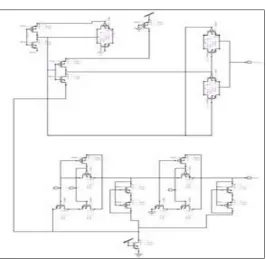
Proposed design is as shown in Fig.2 working of proposed design adder is same as previous adder. Only differences is that we implement carry circuit bi transmission gate logic. As is notable, the fast increment in deferral in transmission gate viper chain keeps the TG topology from being utilized as a part of long Full Adder chains, in light of the fact that the delay turns out to be unsatisfactorily high. Be that as it may, as the TG topology offers a decent speed execution and low power utilization in short Full Adder fastens it bodes well to embrace a blended topology approach, where the TG chains are hindered by the intermitted inclusion of a static door having driving ability. In given circuit we can replace carry circuit with other techniques as it was taking large number of transistor due to which power, area, PDP of overall circuit increases.
Fig. 3: Design of 2-bit multiplier using proposed full-adder
Among the Full Adder topologies without driving capability, the TG adder is the fastest and has the lowest power consumption[7].
So, here we implement carry circuit with transmission gate which gives low transistor count for implementation.
Moreover half adder circuit made in sum circuit can be used in XOR operation in carry circuit, which further reduces transistor size.
Also fig.3 shows design of 2-bit multiplier using proposed full-adder.
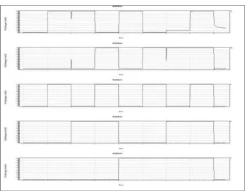
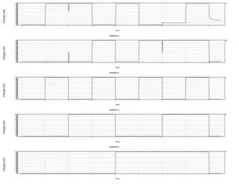
III. SIMULATION RESULTS AND WAVEFORM
(IJSTE/ Volume 4 / Issue 11 / 006)
Simulation were performed using Tanner EDA tool using 90nm TSMC technology file. Fig.4 and Fig. 5 shows simulation result for previous design and proposed design respectively. Obtained results are plotted in table and compare design with previous work. We find out separate delay for sum as well as carry circuit also static power is calculated for separate input all 1 and 0.
Table – 1
Comparison table for adder design
PARAMETERS BASE DESIGNS MODIFIED DESIGNS
POWER (uW) 1.8317 0.9737
DELAY SUM (ps) 36.271 60.922
DELAY CARRY(ps) 92.638 21.207
PDP SUM (aj) 66.437 59.32
PDP CARRY (aJ) 169.68 20.65
STATIC 0 POWER (nW) 23.606 20.926
STATIC 1 POWER (nW) 33.255 33.362
STATIC POWER (nW) 27.9305 27.144
The above table shows the comparison between the previous conventional adder and the proposed modified full adder. And the improvement is quite evident.
Fig. 5: Simulation results of proposed full-adder IV. CONCLUSION
As we are moving towards low power high speed device technology due to shrink in technology size it is very important to be device consume less power and high speed. A low power high speed adder is proposed in this paper. Here due to transmission gate we obtain large reduction in power delay and PDP. Proposed adder is used for application of making high speed multiplier which consume less power.
REFERENCES
[1] Ilham Hassoune, Denis Flandre, “ULPFA : A New Efficient Design of a Power Aware Full Adder,”IEEE Transactions on circuits and systems, Vol 57,no.8 ,August 2010.
[2] R. Singh, “New high performance low power 4 bit full adder with reduce ground bounce noise,” IEEE Conference sept 2013.
[3] I. S. Abu-Khater, A. Bellaouar, and M. I. Elmasry, “Circuit techniques for CMOS low-power high-performance multipliers,” IEEE J. Solid-State Circuits, vol. 31, no. 10, pp. 1535–1546, Oct. 1996.
[4] H. Lee and G.- E. Sobelman, “A newlow-voltage full adder circuit,” in IEEE Proc. 7th Great Lakes Symp. VLSI, 1997, pp. 88–92.
[5] C.-H. Chang, J. Gu, and M. Zhang, “A review of 0.18 m full adder performances for tree structured arithmetic circuits,” IEEE Trans. Very Large Scale Integr. (VLSI) Syst., vol. 13, no. 6, pp. 686–694, Jun. 2005.
[6] S. Goel, A. Kumar, and M.-A. Bayoumi, “Design of robust, energy-efficient full adders for deep-submicrometer design using hybrid-CMOS logic style,” IEEE Trans. Very Large Scale Integr. (VLSI) Syst., vol. 14, no. 12, pp. 1309–1321, Dec. 2006.
[7] M. Alioto “Mixed Full Adder topologies for high performance low power arithmetic circuits”, microelectronics journal, vol38, issue 1 Jan. 2007.
[9] I. Hassoune, A. Neve, J. Legat, and D. Flandre, “Investigation of low-power low-voltage circuit techniques for a hybrid full-adder cell,” in Proc. PATMOS, 2004, pp. 189–197, Springer-Verlag.
[10] C. Piguet, , C. Piguet, Ed., “Chapter 7: Logic Circuits and Standard Cells,”inLow-power Electronics Design. Boca Raton, FL: CRC Press, 2004.
[11] J.-M. Wang, S.-C. Fang, and W.-S. Feng, “New efficient designs for XOR and XNOR functions on the transistor level,” IEEE J. Solid-State Circuits,vol. 29, no. 7, pp. 780–786, Jul. 1994.
[12] V. Dessard, “SOI specific analog techniques for low-noise, high-temperature or ultra-low power circuits,” Ph.D. Thesis, UCL, Louvain, Belgium, 2001. [13] D. Levacq, C. Liber, V. Dessard, and D. Flandre, “Composite ULP diodefabrication, modeling and applications in multi- FD SOI CMOS technology,”Solid
State Electron., vol. 48, no. 6, pp. 1017–1025, Jun. 2004.
[14] V. Kilchytska, D. Levacq, L. Vancaillie, and D. Flandre, “On the great potential of non-doped MOSFETs for analog applications in partially-depleted SOI CMOS process,” Solid State Electron., vol. 49, no. 5, pp. 708–715, May 2005.
[15] G. Merrett and B.-M. Al-Hashimi, “Leakage power analysis and comparison of deep submicron logic gates,” in Proc. PATMOS Conf., 2004, vol. [16] C.-H. Chang, J. Gu, M. Zhang, A review of 0.18-/spl mu/m full adder performances for tree structured arithmetic circuits,, IEEE Trans. VLSI Systems 13 (6)
(2005) 686–695.
[17] A. Shams, M. Bayoumi, A novel high-performance CMOS 1-bit fulladdercell, IEEE Trans. Circuits and Systems—Part II 47 (5) (2000) 478–481. [18] H. Mahmoud, M. Bayoumi, A 10-transistor low-power high-speed full adder cell, in: Proceedings of the ISCAS’99, Orlando, USA, June 1999, pp. 43–46. [19] K. Yano, T. Yamanaka, T. Nishida, M. Saito, K. Shimohigashi, A. Shimizu, A 3.8-ns CMOS 16_16-b multiplier using complementary pass-transistor logic,
IEEE J. Solid-State Circuits 25 (2) (1990) 388–395.
[20] K. Yano, Y. Sasaki, K. Rikino, K. Seki, Top-down pass-transistor logic design, IEEE J. Solid-State Circuits 31 (1996) 792–803.
[21] V.G. Oklobdzija, B.R. Zeydel, H.Q. Dao, S. Mathew, R. Krishnamurthy, Comparison of high-performance VLSI adders in the energydelayspace, IEEE Trans. VLSI Systems 13 (6) (2005) 754–758.
[22] L. Heller, W. Griffin, J. Davis, N. Thoma, Cascode voltage switch logic: a differential CMOS logic family, in: Proceedings of the IEEE International Solid-State Circuits Conference, 1984, pp. 16–17.
[23] K. Chu, D. Pulfrey, A comparison of CMOS circuit techniques: differential cascode voltage switch logic versus conventional logic, IEEE J. Solid-State Circuits SC-22 (1987) 528–532.