Design and Implementation of Testable Reversible
Universal Shift Register
Parasurama Prof. Dr. Meghana Kulkarni
Department of VLSI Design & Embedded Systems Department of VLSI Design & Embedded Systems Centre for PG Studies, Visvesvaraya Technological,
University, Belagavi, Karnataka, India
Centre for PG Studies, Visvesvaraya Technological, University, Belagavi, Karnataka, India
Abstract
The design of testable universal shift register based on conservative logic is tested for unidirectional stuck-at faults by using two test vectors i.e. all 1’s and 0’s. The important memory element in family of sequential circuits is Universal Shift Register. In this project design of sequential application circuits like Universal Shift Register is done by using reversible gates such as Fredkin, Feynman and Peres gates. The proposed 4*4 reversible universal shift register can identify single missing line stuck at faults in the circuits and also it reduces the quantum cost, delay and garbage outputs as well as testability. The important memory element in family of sequential circuits is Universal Shift Register. In this project design of sequential application circuits like Universal Shift Register is done by using reversible gates such as Fredkin, Feynman and Peres gates. The design of testable universal shift register based on conservative logic is tested for unidirectional stuck-at faults by using two test vectors i.e. all 1’s and 0’s. The proposed 4*4 reversible universal shift register can identify single missing line stuck at faults in the circuits and also it reduces the quantum cost, delay and garbage outputs as well as testability.
Keywords: Flip-Flop, Multiplexer, Reversible Logic, Reversible Gate, Shift Register, Quantum Cost, Garbage Output _______________________________________________________________________________________________________
I. INTRODUCTION
In now day’s reversible logic has been considered as an essential concern for computer design. Revisable gates increasing application of low power devices. Shift Register consists of group of flip flops connected corresponding the information bits can be shifted right are left depending on the selection line. Reversible circuits are of great absorption in the range of low power CMOS design, quantum computing, optical computing and nano-technology. Conservative logic is a logic family that performance the effects that there are an equal number of 1s in the outputs as there are in the inputs. Irreversible computation 1 bit of information lost and fans out problem will affected by conventional gates; result by KTln2 joules of energy dissipation, the K is the Boltzmann’s constant T is the absolute temperature.
Conservative logic sometimes revisable and sometimes used the not be reversible in nature. Zero internal power dissipation advantage to the conservative logic proposed technique. The conservative logic line approach offered by avoids number dead ends, and fan out problem is not allowed in this technique.
Basic of Revisable Gates:
Fredkin gate (CSWAP) Feynman gate(CNOT) Peres gate
Toffoli gate Not gate
Double Feynman gate
Conservative Logic Based Fredkin Gate:
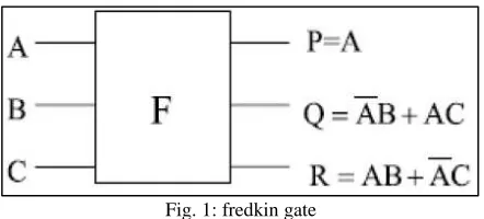
Fig. 1: fredkin gate
Fig 1shows Fredkin gate is a 3*3 gates and universal gate 3 input and 3 output any logical or arithmetic operation done by fredkin gate. The input vector I(A,B,C) & output vector(P,Q,R).the output vector defined (P=A,Q=A′B^AC, And R= A′C ^AB). The quantum cost of fredkin gate is 5.
Related Work:
The design of revisable universal shift register circuits is a addressed in the alternatives interesting augmentation in which designs are enhanced terms of different functions, a like as the number of revisable gates, garbage outputs, quantum cost, delay and testing complexity etc. To the best of our understanding offline testing of revisable universal shift register to shift right are left depending on the design. In this, paper design of Revisable universal shift register that can be tested for two test vectors, all 0’s and all 1’s for any single line missing stuck at faults. By giving both test vectors 0 we test for stuck-at-1 fault and similarly if give the both test vector input are 1 means we test for stuck at-0 fault.
II. DESIGN OF TESTABLE REVISABLE LATHES AND MULTIPLEXER
Design of D Latch:
The D latch characteristic equation written as the Q+=D·E+E’·Q, D is the input of flip flop and E is the enable and Q is the inout
of the flip flop. in the proposed work enable refers to the clock and enable equal in value place of clock. when the enable signal is high the value of the latch output is reflected at the input of D latch the output is Q+=D. while enable is low the output of D latch is Q+=Q.
: Fig. 2: Reversible D latch
Design of Testable Reversible D Latch:
Our proposed work of the two fredkin gate cascade connection the output of first frdkin gate Q while follow the other.and two control signals such as C1 and C2 design the second fredkin gate remaining two inputs.and output of second fredkin gate Q and other one inout terminal and 3rd one garbage output.
Design of 4:1 Multiplexer:
The Multiplexer two control signal S0 and s1used to perform left and right shift and parallel transfer the input data. the multiplexer selected line S1S0=00 present value of the input and select line S1S0=01 shift left, and S1S0=10 shift right operation and S1S0=11Parallel loading operation.
Fig. 4: 4:1 multiplexer using fredkin gate
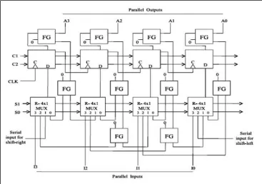
III. DESIGN OF REVISABLE UNIVERSAL SHIFT REGISTER
If the register is there shift that can shift the data in only one direction, either from left to right or from left they can call it unidirectional shift register. The register that can shift the data in both directions from left to right and right to left they call it bidirectional shift register. have the bidirectional shift register as well as the parallel loading then that shift register is called universal shift register. Parallel loading means the data stored in the flip flop input entered into the parallel manner or we can say simultaneously.
Fig. 5: 4 bit Reversible universal shift register
Table – 1
Universal shift register mode of operation Mode control
Register operation
S1 S0
The multiplexer two control signal S1 and S0, which is used to perform the operation of shift left, right parallel loading. the input value S1S0=00 No change the register operation the multiplexer selected input 0.The input value S1S0=01 multiplexer selected input 1and thus the right shift operation take place. The input value S1S0=10 multiplexer selected input 2 and thus the left shift operation take place. When the select line S1S0=11 the multiplexer selected input 3 and thus the parallel load operation take place in universal shift register
Table – 2
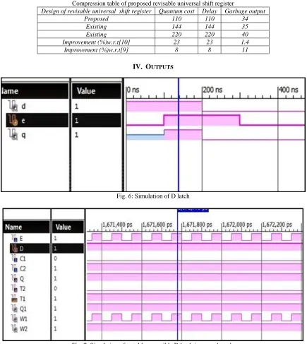
Compression table of proposed revisable universal shift register
Design of revisable universal shift register Quantum cost Delay Garbage output
Proposed 110 110 34
Existing 144 144 35
Existing 220 220 40
Improvement (%)w.r.t[10] 23 23 1.4
Improvement (%)w.r.t[9] 8 8 11
IV. OUTPUTS
Fig. 6: Simulation of D latch
Fig. 7: Simulation of testable reversible D latch in normal mode
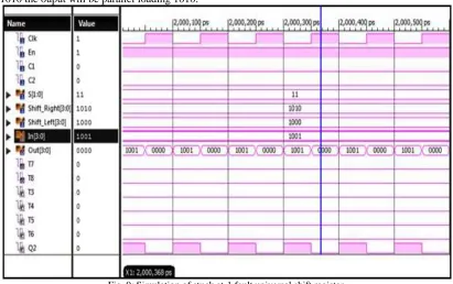
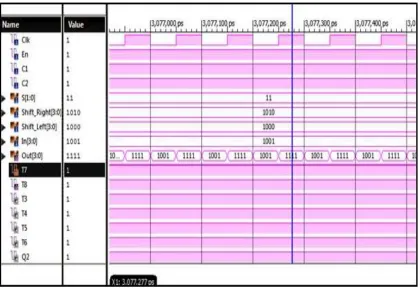
Fig. 8: Simulation of normal mode universal shift register
A universal shift register when the test vectors C1C2=01,the normal mode of shift register and select line is both are high the input will be 1010 the ouput will be parallel loading 1010.
Fig. 9: Simulation of stuck at-1 fault universal shift register.
Fig. 10: Simulation of stuck at-0 fault universal shift register.
A stuck at-0 fault reversible universal shift register,when the test vector C1C2=11 the output of the 4 bit universal shift register all are high.and select line will be high but do not parallel loading becouse stuck at-0 fault of the circuit
V. CONCLUSION
The proposed testable reversable universal shift register uses conservative logic method to teste for any stuck at fault by using two test vectors named as 0s and 1s. In this method reversible flip flop circuits are employed for designing complex sequintial circuits of universal shift register The proposed method can be applied in the real time application of fault coverage by single missing /additional cell and in testing sequential circuits. The proposed method uses less number of reversible gates in order to reduce circuit complexity.This method in turn reduces the number garbage outputs 1.8%, quantum cost 22%, dealy 22% and testablity complexity.
VI. FUTURE SCOPE
1) This method further can be applied for combinational circuits such as datapath elements viz, adders, substructors, mutiplers and encoder, decoder design and compartor design.
2) By incresing bit size in the universal shift register this method can be employed in designing counter circuits.
3) Further this method of testability can be applied for a complete Processor design using reversible logic components and using revesable instruction set.
4) This method can also be applied for Multi-Core Processor Design.
REFERENCES
[1] 1Prasanna.M and 2Amudha.S, ‘‘implementation of testable reversible sequential circuits on FPGA,’’ IEEE Sponsored 2nd International Conference on Innovations in Information Embedded and Communication Systems ICIIECS’15.
[2] 1K.Rekha swathi sri,2M.Mano,3 G.Selvapriya, ‘‘Reversible gate based testable sequential circuits,’’ Proceedings of International Conference on Global Innovations in Computing Technology (ICGICT’14).
[3] 1Papiya Biswas, 2Namit Gupta, 3Nilesh Patida, ‘‘Basic Reversible Logic Gates and its Qca Implementation,’’ Papiya Biswas et al Int. Journal of Engineering Research and Applications ISSN: 2248-9622, Vol. 4, Issue 6(Version 5), June 2014, pp.12-16.
[4] 1Amita Nandal and 2 T.Vigneswaran‘‘FPGA implementation of efficient combinational and sequential logic design using testable reversible logic,’’ Available online at www.elixirpublishers.com (Elixir International Journal).
[5] 1Shaunk Basu and 2 Subhashree Basu, ‘‘Reversible Logic Synthesis of Sequential Circuits,’’ International Journal of Computer Applications (0975 – 8887) Volume 129 – No.11, November2015.
[7] M. Diana Amutha Priya and R. Arun Prasath, ‘‘Testing of stuck at faults in reversible sequential circuits using verilog HDL,’’ ARPN Journal of Engineering and Applied Sciences VOL. 10, NO. 7, APRIL 2015.
[8] 1Rashid Anwar, 2 Jobbin Abraham Ben, ‘‘A Novel Design of Reversible Universal Shift Register,’’ Rashid Anwar et al, International Journal of Computer Science and Mobile Computing, Vol.3 Issue.3, March- 2014.
[9] Ashis Kumer Biswas, Lafifa Jamal, M. A. Mottalib1, Hafiz Md. Hasan Babu.” Design of a Reversible Parallel Loading Shift Register” .Dhaka Univ. J.Eng & Tech. vol 1(2) 1-5,2011