Abstract: DMTGDI is introduced an ultra-low power, high speed dual mode cmos logic family. It mainly improves characteristics of gate diffusion sub-threshold circuit design. A dmtgdi of type a and type b design was implemented in cmos logic circuits and the proposed configuration was employed in a single bit full adder was implemented in 10t configuration to analyses the performance through the simulations. During the simulation minimum delay was obtained with the help of proposed dmtgdi technique and its consume the minimum amount of power. In dmtgdi 60% performance improvement has been done in over conventional dml, and significant reduces power-delay product (pdp), both in dynamic mode, static mode 95%, and 75% respectively. Layout simulation performance is done in single bit adder. Tgdi gates are implemented additionally because this is the previous version of dmtgdi. The proposed architecture was implemented in cadence virtuoso with 180nm width of cmos logic and the post simulation was obtained through asura.
Keywords: cmos, dmtgdi, mep, dml, pdp
I. INTRODUCTION
In recent years, battery powered mobile devices have been increased rapidly and almost every moments of our lives has been changed by modern portable technologies. Therefore ultra low power devices and circuits is extremely important. The sub-threshold circuit in power consumption is one of the most common methods for reducing consumption of power, because minimum energy point (MEP) of a digital system [1]. Here transient response of both the DMTGDI and full adder using DMTGDI is designed using CMOS logic then layout design for an full adder circuit using 10 transistor. But circuits in sub-threshold region have more constraints and sensitivities in threshold operation [2-3]. Here one bit full adder in DMTGDI is going to design using cadence software.
II. SUBTHRESHOLD DUAL MODE LOGIC
Dual mode logic (DML) gates family enhance a very high level of energy delay optimization easy to the gate level recently. This flexibility is used to improve energy efficiency and performance of combinatorial circuits.
Gate diffusion input is a advanced technique of low-power digital combinatorial circuit design is described. This technique also reduces power consumption, propagation delay, and area of digital circuits while maintaining low complex of logical design. Several logic circuits have been implemented in various design styles[4]. Their properties, simulation results, and measurements of a test chip are discussed, reported and presented respectively. Also total power consumption can be decreased by setting gates on the critical path in dynamic mode and setting the rest of the circuit in static mode[5].
III. OVERVIEW: DMTGDI
A. TGDI cell structure
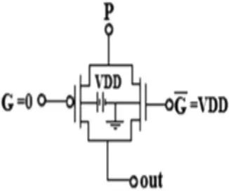
Figure 1: (a) GDI cell. (b) TGDI cell. (c) TGDI cell (with complimentary outputs).
Figure 2: Upper half of TGDI circuit.
B. TGDI circuits
At first glance, GDI structure Figure. 1a reminds the standard CMOS inverter it will have a main difference is that the GDI cell contains three inputs (G, P and N) and it will simply changes the input configuration of the simple GDI cell similar to very different. Actually, GDI (an also TGDI) logic is some kind of pass transistor logic but the main difference is that in pass transistor or transmission gate logics the top-down logic design is so difficult, which predict production of a simple and universal cell library with these logics[7]. Performance of implemented adder in DMTGDI logic has been enhanced by methods of DML [8]. Pre-charging is performed by a minimum sized M1 transistor and its parallel network acts as an active keeper, which provides more robustness in comparison with domino logic [9], and also solves some drawbacks of domino logic such as crosstalk noise, charge sharing and sensitivity to glitches [10].
IV. IMPLEMENTATION OF DMTGDI
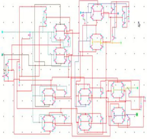
By using dynamic logics, like domino, performance of digital circuits can be incredible increased, but high sensitivity of dynamic logics to process variations. It is unsuitable for nano scale technologies. First we design the 40T in DMTGDI circuit that output is shown in figure 3. Difference between the type A and type B is pmos will be in upper half of the circuit and nmos in lower half of the circuit respectively. For type a and type B 5 transistor each. Here pulse wave is give as the input of both the circuit.
[image:3.612.222.385.296.435.2]Figure 3: simulation output of 10 Transistor (10T) full adder with DMTGDI logic
Figure 4: One bit full adder (40T) in DMTGDI logic
V. RESULTS AND DISCUSSION
In conventional DML, GDI, TGDI and DMTGDI logics a single bit full adder which demonstrated, has been implemented. According to optimal design in DML enhanced by connecting cascaded gates in type A and B alternatively. The entire circuit was operating at 1.8V and the output of 10T in DMTGDI logic is shown in Figure 5.
[image:4.612.184.430.375.607.2]Figure 5:simulation output of 10 Transistor full with DMTGDI logic.
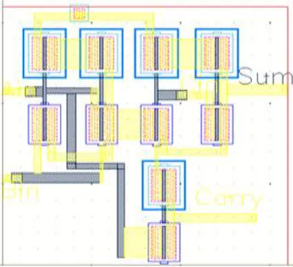
Simulation results of full adder are shown in Figure 5. Also speed of DMTGDI logic in dynamic and static mode has improved about 60% in comparison with corresponding modes in conventional DML. The simulation output of one bit full adder in DMTGDI shown in Figure 6. Layout design of an full adder in designed and it is shown in figure 7. Area occupied by an full adder in this design is 188µm. power consumption of an full adder circuit 7.912mW. All cells have been designed in the form of standard cells with equal heights and regulated routing junctions figure 4. There will be a slight variation in the sum output signal. Figure 7 is layout design of an 10T full adder circuit plus 3 transistor is used of DMTGDI logic. In cadence tool for transient response we have to manually feed the time duration here 100ns time gap with in that duration output signal will be generated.
[image:5.612.199.411.337.468.2] [image:5.612.199.412.499.693.2]VI. CONCLUSION
DMTGDI is a new logic family has been introduced in based of two consecutive steps. Type A and type B circuit is integrated with a two single bit adder circuits such as traditional adder circuit (40T) and the modified adder circuit (10T) is designed to obtain the simulation results. In this circuit the delay was minimized 3.76% compared with the GDI technique. In other hand the power consumption is decreased 0.8 mW. Finally the proposed 10T based modified adder circuit consume the area 188µm, so the proposed architecture is suitable for high speed operation in digital circuits.
REFERENCES
[1] M. Alioto, Ultralow power VLSI circuit design demystified and explained: a tutorial, IEEE Trans. Circuits Syst.I59(1)(2012)3–29.
[2] M. Alioto, Understanding DC behavior of sub-threshold CMOS logic through closed-form analysis, IEEE Trans. Circuits Syst.57(7)(2010)1597–1607.
[3] S. Kumar Gupta, A. Ray chowdhury , K. Roy, Digital computation in sub-threshold region for ultralow-power operation: a device–circuit–architecture co design perspective, Proc. IEEE 98 (2) (2010)160–190.
[4] Jan M. Rebaey, Digital Integrated Circuits: A Design Perspective, second .,2012 (Chapter 3).
[5] I. Levi, A. Fish, Dual mode logic-design for energy efficiency and high performance, IEEE Access 1 (2013) 258–265.
[6] Ryan D. Jorgenson, Lief Sorensen, Dan Leet, Michael S. Hagedorn, David R. Lamb, Thomas Hal Friddell, Warren P. Snapp, Ultralow-power operation in subthreshold regimes applying clockless logic, Proc. IEEE 98 (2010) 299–314.
[7] A. Morgenshtein, A. Fish, I.A. Wagner, Gate-diffusion input (GDI): a power efficient method for digital combinational circuits, IEEE Trans. Very Large Scale Integr. (VLSI) Syst. 10 (5) (2002)
[8] I. Levi, O. Bass, A. Kaizerman, A. Belenky, and A. Fish, High speed dual modelogic carry look ahead adder,in: Proceedings of the IEEE International Symposium on Circuits and Systems (ISCAS), May 2012, pp. 3037–3040
[9] I. Levi, A. Kaizerman, A. Fish, Low voltage dual mode logic: model analysis and parameter extraction, Microelectron. J.44 (2013) 553–560.
[10] A. Kaizerman, S. Fisher, A. Fish, Subthreshold dual mode logic, IEEE Trans. Very Large Scale Integr. (VLSI) Syst. 21 (5) (2013) 979–983.
AUTHOR DETAILS
D.Yokeshwari is presently pursuing Master degree in VLSI Design at Tejaa Shakthi institute of Technology, Coimbatore. She has interested in Low power VLSI design and Digital signal processing