Technology (IJRASET)
Design and Simulation of Four Input Buck
DC-DC Converter using MATLAB/Simulink
A.Thiyagarajan1 1
Assistant Professor, Department of E.E.E, Karpagam Institute of Technology, Coimbatore, Tamilnadu, India
Abstract— DC-DC buck converters are used to step down the input DC voltage to maintain a required voltage in a renewable energy system. In this paper, we proposed four input buck DC-DC converter which can be used to improve efficiency, performance and also to reduce cost and component count of the DC-DC converter. Four input buck dc-dc converter is designed through derivation by using five Single pole Single Throw (SPST) switches as a building block. Switch realization and operating characteristics of proposed four input buck dc-dc converter is obtained with their voltage transfer ratios in buck mode of operation with constant voltage. The performances of the proposed dc-dc converter are tested with the simulation results using MATLAB/Simulink.
Keywords—DC-DC Buck converter, Single pole single throw Switch, modes of operation, Voltage transfer ration, MATLAB/Simulink.
I. INTRODUCTION
The aim of this paper is to design a four input dc–dc buck converter to provide an interface between multiple DC sources and a single DC output. The conventional approach of connecting the energy storage unit is by using independent converter has many difficulties [5]. The independent converter with energy sources can be connected either in series or parallel in multiple input converters. If the sources are connected in series it has to conduct the same current and if the converters are connected in parallel it should have same Voltage levels [6]-[8]. Both the conditions are practically undesirable and the converter controller design is also difficult [9][10]. Instead of this, multi input converter is used to connect multi voltage Sources in a single converter system to give required load requirement an also to improve efficiency [11], reduce overall cost, reduce component count, more stability and simple control. In this Paper, only four inputs are used. So it is named as four input dc-dc buck converter. Multi input converters can be constructed using either flux additivity [12] by using a multi input transformer which has multi tap in primary windings or by combining the structure of the converters. There is not a systematic approach to design multi input converters through derivation [1]. Design of new converters from existing converters is complicated task [2]. Hence in this paper, a systematic approach is given to design a proposed converter through derivation by using four Single pole Single Throw (SPST) switch as building block. The Fig.1 shows the block diagram of four input dc-dc buck converter with four input voltage sources.
Fig.1 Block diagram of four input dc-dc buck converter
Simulation model and results of the proposed converter are presented in part IV.
II. FOURINPUTDC-DCBUCKCONVERTERUSINGFIVESINGLEPOLESINGLETHROWSWITCH
The basic circuit diagram of the proposed four input buck dc-dc converter using five single pole single throw switch as a building block is shown in Fig.2.
Fig.2 A Basic circuit diagram of four input buck dc-dc converter using Five Single Pole Single Throw switch
Voltage source V1 delivers power to load when the switch is ON. Voltage source V2 delivers power to load when the switch is ON. Similarly N- number of voltage sources delivers power to the load when the particular channel switch is ON. It consists of five SPST switches S1, S2, S3, S4, S5 which can be turned ON and OFF individually. The switching patterns of the five switches are shown in Fig.3.
Fig.3 Switching patterns of four input buck dc-dc converter using five Single Pole Single Throw switch
Technology (IJRASET)
TABLE I MODES OF OPERATION OF FOUR INPUT BUCK DC-DC CONVERTER
Modes ON condition switches OFF condition switches Voltage across Inductor(VL)
1 S1 S2,S3,S4,S5 V1-V0
2 S2 S3,S4,S5,S1 V2-V0
3 S3 S4,S5,S1,S2 V3-V0
4 S4 S5,S1,S2,S3 V4-V0
5 S5 S1,S2,S3,S4 -V0
In mode 1, V1 gives energy to the inductor and load resistor R. In mode 2, V2 gives energy to the inductor and load resistor
R .In mode 3, V3 gives energy to the inductor and load resistor R. In mode 4, V4 gives energy to the inductor and load resistor R.
In mode 5, all the input voltage sources are disconnected from the circuit. The energy stored in the inductor is being released to the load. The energy stored in the inductor is reenergized during this mode.
Voltage transfer ratio
It can be formed by taking the product of individual switch duty ratios and total time from the switching patterns.
Where,
T - Total time period of the switching patterns.
d1, d2 , d3 ,d4 and d5 - duty ratios of the switches S1 , S2 ,S3 ,S4 and S5 respectively.
V1 V2 V3 V4 and V5 - Input voltage of the converter.
V0 - output voltage of the converter.
T1, T2 ,T3 ,T4 and T5 -On time of the switches S1 ,S2 ,S3 ,S4 and S5 respectively.
.
Voltage second balance equation of the inductor is given by
(7)
(8)
(9)
By combining the equations (1), (2), (3), (4),(5) and (6), we can get the voltage transfer ratio of the following equation (10) which gives the relation between the input and output of four input buck dc-dc converter.
(10)
III.SWITCHREALIZATIONOFFOURINPUTBUCKDC-DCCONVERTER
Fig.4 The circuit diagram of three input buck-boost dc-dc converter
The circuit diagram of the proposed four input dc-dc buck converter is shown in Fig.4.Voltage drop across the inductor depends on the switches which are in ON condition.S1, S2, S3, S4 and S5 conducts positive current and opposes either positive or negative voltage depending on the magnitude of input voltages. For this purpose, the switches are replaced by diode is connected series with MOSFET.It is necessary to commutate the switches with each other depending upon the modes. In this converter, it uses only one Inductor [13],[14]. Switch S5 which conducts positive current and opposes negative voltage, so it can be replaced only by diode. The basic idea in the synthesis of the proposed four input dc-dc buck converter is to bring a new switching circuit which can be able to connect or disconnect input voltage sources individually or simultaneously [15]. Inductor is used as an energy storage element in this circuit [3], [9].
IV.SIMULATIONMODELANDRESULTSOFFOUR INPUTBUCKDC-DCCONVERTER
The simulation model and the output results are verified using MATLAB/simulink. The simulation model of four input buck dc-dc converter is shown in the Fig.5.
Fig.5 Simulation model of four input buck dc-dc converter using MATLAB
Technology (IJRASET)
in continuous conduction mode (CCM). The converter is switched by signal having duty ratio with phase shifted by an angle 90 degrees between each switches at a switching frequency of 100 kHz. Pulse width modulation technique is used in this
converter. The simulation result of switching signals for Switches S1, S2 , S3 ,S4 of four input buck dc-dc converter in boost
mode is shown in the Fig.6. The simulation result of inductor voltage in buck mode is shown in Fig.7. The simulation result of Input current of each input voltage source in buck mode is shown in Fig.8
Fig.6 Switching signals of four input buck dc-dc converter (sum of duty ratios=0.4) using MATLAB
Fig.7 Inductor voltage of four input buck dc-dc converter (sum of duty ratios=0.4) using MATLAB
Fig.8 Input current of four input buck dc-dc converter (sum of duty ratios=0.4) using MATLAB
The simulation result of Output current in buck mode is shown in Fig.9 The simulation result of Output voltage in buck mode is
shown in Fig.10. The simulation result switching signals for Switches S1, S2 , S3 ,S4 of four input dc-dc buck converter in buck
Fig.9 Output current of four input buck dc-dc converter (sum of duty ratios=0.4) using MATLAB
Fig.10 Output voltage of four input buck dc-dc converter (sum of duty ratios=0.4) using MATLAB
Fig.11 Switching signals of four input buck dc-dc (sum of duty ratios=2) using MATLAB
The simulation result of Inductor voltage in buck mode dc (sum of duty ratios=2) is shown in Fig.12. The simulation result of Input current of each input voltage source in buck mode dc (sum of duty ratios=2) is shown in Fig.13. The simulation result of Output current in buck mode dc (sum of duty ratios=2) is shown in Fig.14
Technology (IJRASET)
Fig.13 Input current of four input buck dc-dc converter (sum of duty ratios=2) using MATLAB
Fig.14 Output current of four input buck dc-dc converter(sum of duty ratios=2) using MATLAB
Fig.15 Output voltage of four input dc-dc buck (sum of duty ratios=2) using MATLAB
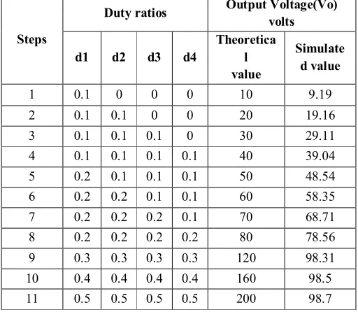
TABLE II. COMPARISON OF OUTPUT VOLTAGE OF FOUR INPUT DC-DC BUCK-CONVERTER AT VARIOUS DUTY RATIOS
Steps
Duty ratios Output Voltage(Vo) volts
d1 d2 d3 d4
Theoretica l value
Simulate d value
1 0.1 0 0 0 10 9.19
2 0.1 0.1 0 0 20 19.16
3 0.1 0.1 0.1 0 30 29.11
4 0.1 0.1 0.1 0.1 40 39.04
5 0.2 0.1 0.1 0.1 50 48.54
6 0.2 0.2 0.1 0.1 60 58.35
7 0.2 0.2 0.2 0.1 70 68.71
8 0.2 0.2 0.2 0.2 80 78.56
9 0.3 0.3 0.3 0.3 120 98.31
10 0.4 0.4 0.4 0.4 160 98.5
11 0.5 0.5 0.5 0.5 200 98.7
[image:9.612.178.434.93.316.2]The comparison of theoretical and simulated value of output voltage of the four input dc-dc buck converter in various steps is shown in Fig.16.
Fig.16 Comparison of theoretical and simulated value of output voltage of the four input dc-dc buck converter in various steps
It is observed that if the sum of the duty ratios is above. (d1=d2=d3=d4=1.2), the converter maintains constant output voltage. So it will provide constant regulated output voltage. Here the converter is designed and tested in open loop configuration. The
performance of the converter is simulated under constant input voltages (V1=V2=V3=V4=30V).The converter is simulated with
the duty ratio is 0.1 for all the switches (sum of duty ratio is 0.4).
V. CONCLUSION
Technology (IJRASET)
REFERENCES
[1] Karteek Gummi, Mehdi Ferdowsi,”Derivation of New Double-Input DC-DC Converters Using H-Bridge Cells as Building Blocks IEEE Trans. Power Electron, 2008.pp. 2806-2811.
[2] Karteek Gummi, Mehdi Ferdowsi,”Double-Input DC–DC Power Electronic Converters for Electric-Drive Vehicles—Topology Exploration and Synthesis Using a Single-Pole Triple-Throw Switch” IEEE Trans. Power Electron, Feb 2010, vol. 57, NO. 2
[3] K. Hirachi, M. Yamanaka, T. Takada, T. Mii, M. Nakaoka, “Feasible developments of utility-interactive multi-functional bidirectional converter for solar photovoltaic generating system incorporating storage batteries,”IEEEPower Electronics Specialists Conference, 1995, vol. 1, pp. 536-541
[4] K. W. Ma, Y. S. Lee, “An integrated fly back converter for DC uninterruptible power supply,” IEEE Transactions on Power Electronics, 1996, vol.11, pp. 318-327.
[5] Y. M. Chen, Y. C. Liu, F. Y. Wu, “Multi-input DC-DC converter based on the multi-winding transformer for renewable energy applications,” IEEE Transactions on Industry Applications, 2002, vol. 38, pp. 1096-1104.
[6] A. D. Napoli, F. Crescimbini, S. Rodo, L. Solero, Multiple input DC-DC power converter for fuel-cell powered hybrid vehicles,” IEEE Power Electronics Specialists Conference, 2002, vol. 4, pp. 1685-1690.
[7] . Solero, A. Lidozzi, J. A. Pomilio,“Design of multiple-input power converter for hybrid vehicles,” IEEE Transactions on Power Electronics, 2005, vol. 20, pp. 1007-1016.
[8] S. Arulselvi, K. Deepa, G. Uma, “Design, analysis and control of a new multi output fly back CF-ZVS-QRC,” International Conference on Industrial Technology, 2005, pp. 413-418.
[9] K. Kobayashi, H. Matsuo, Y. Sekine, “Novel Solar-Cell Power Supply System Using a Multiple-Input DC–DC Converter,” IEEE Industrial Electronics Transactions, 2005, vol. 53, pp. 281-286.
[10] K. P. Yalamanchili, M. Ferdowsi, “Review of multiple input DC-DC converters for electric and hybrid vehicles,” Vehicle Power and Propulsion IEEE Conference, 7-9 Sept 2005,. pp. 160-163.
[11] Y. M. Chen, Y. C. Liu, S. H. Lin, “Double-Input PWM DC/DC Converter for High/Low-Voltage Sources,” IEEE Transactions on Industrial Electronics, 2006, vol. 53, pp. 1538-1545.
[12] D. Liu, H. Li, “A ZVS Bi-Directional DC–DC Converter for Multiple Energy Storage Elements,” IEEE Transactions on Power Electronics, 2006, vol. 21, pp. 1513-1517.
[13] Y. M. Chen, Y. C. Liu, and F. Y. Wu, “Multi-input converter with powerfactor correction, maximum power point tracking, and ripple-free input currents,” IEEE Trans. Power Electron., May 2004. vol. 19, no. 3, pp. 631–639