energies
Article
Near State Vector Selection-Based Model Predictive
Control with Common Mode Voltage Mitigation for a
Three-Phase Four-Leg Inverter
Abdul Mannan Dadu1 ID, Saad Mekhilef1,*, Tey Kok Soon2, Mehdi Seyedmahmoudian3 ID and Ben Horan3 ID
1 Power Electronics and Renewable Energy Laboratory, Department of Electrical Engineering, University of Malaya, Kuala Lumpur 50603, Malaysia; [email protected]
2 Department of Computer System & Technology, University of Malaya, Kuala Lumpur 50603, Malaysia; [email protected]
3 School of Engineering, Deakin University, Waurn Ponds, Victoria 3216, Australia; [email protected] (M.S.); [email protected] (B.H.) * Correspondence: [email protected]; Tel.: +60-37-967-6851
Received: 25 October 2017; Accepted: 8 December 2017; Published: 14 December 2017
Abstract:A high computational burden is required in conventional model predictive control, as all of the voltage vectors of a power inverter are used to predict the future behavior of the system. Apart from that, the common mode voltage (CMV) of a three-phase four-leg inverter utilizes up to half of the DC-link voltage due to the use of all of the available voltage vectors. Thus, this paper proposes a near state vector selection-based model predictive control (NSV-MPC) scheme to mitigate the CMV and reduce computational burden. In the proposed technique, only six active voltage vectors are used in the predictive model, and the vectors are selected based on the position of the future reference vector. In every sampling period, the position of the reference current is used to detect the voltage vectors surrounding the reference voltage vector. Besides the six active vectors, one of the zero vectors is also used. The proposed technique is compared with the conventional control scheme in terms of execution time, CMV variation, and load current ripple in both simulation and an experimental setup. The LabVIEW Field programmable gate array rapid prototyping controller is used to validate the proposed control scheme experimentally, and demonstrate that the CMV can be bounded within one-fourth of the DC-link voltage.
Keywords:near state vector selection based model predictive control; common mode voltage; ripple content; execution time; computational burden and three phase four leg inverter
1. Introduction
Photovoltaic (PV) energy has become an attractive renewable energy source due to its user-friendly operation, straightforward structure, easy installation, and close setup to the user. In PV energy conversion and distribution systems, three-phase four-leg inverters are becoming popular in specific
applications such as standalone [1] and Uninterruptible power supply (UPS) systems [2], as well
as in islanded mode when the grid supply has failed [3]. A standalone PV system has to provide
uninterrupted and balanced/unbalanced power for utilities such as data communication, aircraft,
home appliances, satellite stations, and railway systems [4]. However, delivering an unbalanced load
is a commercial and industrial issue in an energy conversion system. A four-wire three-leg inverter can be used to deliver unbalanced power, but it has the drawback of low utilization DC-link voltage. The potential difference between the star point and the midpoint of DC-link capacitors is forced to zero; therefore, the star point of the load is not free [5,6]. Thus, four-leg inverters have been introduced
that can provide zero sequence paths, and are thus preferred over three-leg inverters to distribute power to the balanced/unbalanced loads. Moreover, three-phase four-leg inverters can overcome the
low voltage DC-link utilization of the three-phase four-wire system [7]. Due to the additional leg,
the control vectors increase from 8 (23) to 16 (24), which increases the number of switching actions in
every switching period [8–10]. However, the common mode voltage (CMV) between the load-neutral
point and the midpoint of the DC-link capacitors of the three-phase four-leg inverter causes radiation
in the electromagnetic interference, system losses, and threats to personal safety [11].
In order to overcome these problems, the CMV has to be mitigated or reduced. This can be achieved actively or passively. In active mitigation, active circuits such as transistors and capacitors
are used. Meanwhile, passive components are used in passive mitigation [12]. Owing to hardware
additions or modifications, these methods lead to increases in size and higher costs, and thus cannot be directly applicable to high-voltage systems. Thus, research is progressing towards software invention or modification through improving the control algorithm. The improvement in software can be divided into two main types. The first type is achieved with a modulation-based control algorithm. In a
three-phase four-leg inverter, CMV can be kept constant at ±vdc
2 (vdc is the DC-link voltage) by
improving the modulation mode with the Boolean logic function [13]. A pulse width modulation
(PWM) block that avoids the zero-voltage vector has been introduced to alleviate the CMV in [14].
A control scheme with six switching states for the three-phase four-leg inverter is proposed to ensure
the zero CMV in [15]. However, this switching scheme cannot be practically implemented for the
unbalanced condition due to the utilization of the restricted voltage vector in a conventional method. The aforementioned PWM-based control algorithms consist of a modulation stage and an inner control loop with proportional–integral (PI) controllers. In the second type of improvement scheme, an easier and more powerful control method, the finite control set model predictive control (FCS-MPC) is used. The FCS-MPC considers a finite number of valid switching states to predict the behavior of the system
through a discrete model in every sampling period [16–19]. The FCS-MPC uses a cost function to carry
out the optimization in the prediction. The predefined cost function is used to compare each prediction with its respective reference, and the switching state that produces the minimum value of the cost function is applied to the inverter. This process is repeated in every sampling period as mentioned
in [9,20–22], and thus, no modulation stage is required in this technique. The implementation of
the FCS-MPC is very easy and simple, and it has fast a dynamic response in spite of its constraints
and nonlinearity inclusion [8,23–25]. However, since the FCS-MPC algorithm predicts the control
variables based on the system model, it puts a high computational burden on the controller [20,26,27].
This FCS-MPC-based control technique also can be used to restrict the CMV within±vdc
6 by utilizing
six non-zero voltage vectors in the three-phase three-leg inverter [28]. The FCS-MPC method can
reduce the CMV and control the load current for the three-phase three-leg inverter, as mentioned
in [28–30]. Meanwhile, in [29], the load current ripple and CMV are reduced, but the process of
selecting two non-zero voltage vectors in each sampling period and determining each vector duration
is very complex. This greatly increases the computation complexity. Guo et al. [31] proposed the use of
four non-zero voltage vectors in order to reduce the CMV for three-phase three-leg inverters to±vdc
6 ,
but the complicated switching selection between opposite voltage vectors increases the switching
losses. In [32], the CMV factor is inserted into the cost function in order to reduce the CMV, but this
increases the ripple content in the load current. In recent works, there is a lack of CMV mitigation with reduced computational burden, and most of the research studies have focused on the three-phase three-leg inverter. Thus, further research work is required for the three-phase four-leg inverter.
causing a high CMV. Thus, only six switching states are required to predict the future voltage vector. Consequently, only six repeated iterations are required in every sampling period, which reduces the computational burden.
The rest of this paper is structured as follows: the mathematical models for the inverter-load
system are derived in Section2. Then, the model predictive control for three-phase four-leg inverter is
explained in Section3, and the proposed control technique is described in Section4. The proposed
system is then validated through simulation, and the experimental results are given in Section5.
Afterwards, the robustness and performance analysis are discussed in Section6. Then, the appropriate
conclusions are drawn in Section7.
2. Three-Phase Four-Leg Inverter Model
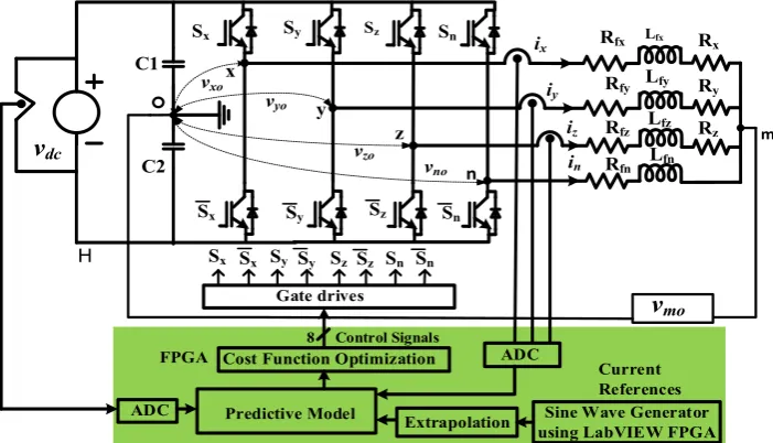
A three-phase four-leg inverter topology with the output resistive-inductive (R-L) filter is shown
in Figure1. The neutral leg in the inverter topology is used to control the zero-sequence current.
The neutral inductor is introduced in the fourth leg to attenuate the switching current ripple to be the same as the other legs. Besides, the neutral inductor limits the fault current during short circuit or
unbalanced loading conditions [15,33]. Therefore, neutral inductanceLf nis connected at the neutral
leg in the practical applications [34,35].
Energies 2017, 10, 2129 3 of 20
CMV, the zero-switching voltage vector has to be eliminated from the switching state, because it is causing a high CMV. Thus, only six switching states are required to predict the future voltage vector. Consequently, only six repeated iterations are required in every sampling period, which reduces the computational burden.
The rest of this paper is structured as follows: the mathematical models for the inverter-load system are derived in Section 2. Then, the model predictive control for three-phase four-leg inverter is explained in Section 3, and the proposed control technique is described in Section 4. The proposed system is then validated through simulation, and the experimental results are given in Section 5. Afterwards, the robustness and performance analysis are discussed in Section 6. Then, the appropriate conclusions are drawn in Section 7.
2. Three-Phase Four-Leg Inverter Model
A three-phase four-leg inverter topology with the output resistive-inductive (R-L) filter is shown in Figure 1. The neutral leg in the inverter topology is used to control the zero-sequence current. The neutral inductor is introduced in the fourth leg to attenuate the switching current ripple to be the same as the other legs. Besides, the neutral inductor limits the fault current during short circuit or unbalanced loading conditions [15,33]. Therefore, neutral inductance is connected at the neutral leg in the practical applications [34,35].
Sn Sz Sy
Sx Sz
x
y
z
n
Sx
H
m
Sy Sz Sn
v
dcix
in
iy
iz
Rfx
Rfy
Rfz
Rfn Lfx
Lfy
Lfz
Lfn Rx
Ry
Rz
Sx Sy Sz Sn
ADC
ADC Gate drives
Sx Sy Sn
Cost Function Optimization
Predictive Model
Control Signals
Current References 8
FPGA C1
C2 vxo
vyo
vzo
vno
v
mo [image:3.595.122.473.333.534.2]Sine Wave Generator using LabVIEW FPGA Extrapolation
Figure 1.Three-phase four-leg inverter with a field programmable gate array (FPGA) control block.
The paired insulated-gate bipolar transistor (IGBT) switches in each of the four legs turn on and off in a complementary mode. If the upper switch of one leg is turned on, the lower one is turned off, and vice versa. The CMV is the potential difference between the midpoint of the DC-link capacitors and the load-neutral point (vmo), as shown in Figure 1. The CMV can be expressed in terms of the voltage on each leg, as shown in [36]:
= + + +
4 (1)
where , , , and are the voltages between the terminal and the midpoint of the DC-link. Based on the switching states, the phase voltages can have either voltages level + or − .
Therefore, depending on the 16 switching states of the three-phase four-leg inverter, the CMV can have the values ± , 0, and ± .
According to Kirchhoff’s voltage law, the inverter’s output voltages can be written as follows: Figure 1.Three-phase four-leg inverter with a field programmable gate array (FPGA) control block.
The paired insulated-gate bipolar transistor (IGBT) switches in each of the four legs turn on and off in a complementary mode. If the upper switch of one leg is turned on, the lower one is turned off, and vice versa. The CMV is the potential difference between the midpoint of the DC-link capacitors
and the load-neutral point (vmo), as shown in Figure1. The CMV can be expressed in terms of the
voltage on each leg, as shown in [36]:
vmo =
vxo+vyo+vzo+vno
4 (1)
wherevxo,vyo,vzo, andvnoare the voltages between the terminal and the midpoint of the DC-link.
Based on the switching states, the phase voltages can have either voltages level+vdc
2 or−
vdc
2 . Therefore,
depending on the 16 switching states of the three-phase four-leg inverter, the CMV can have the values ±vdc
2 , 0, and ±
vdc 4 .
According to Kirchhoff’s voltage law, the inverter’s output voltages can be written as follows:
v=Rf+R
i+Lf
di
where:
v=h vxH vyH vzHvnH
iT
i=h ix iy iz in
iT
Rf +R= h
Rf x+Rx Rf y+Ry Rf z+RzRf n
iT
Lf = h
Lf x Lf y Lf z Lf n
iT
in+ix+iy+iz =0
where,vis the load voltage vector,iis the load vector current,Rf is the filter resistance,Ris the load
resistance,Lf is the filter inductance, andvmHis the voltage between the load-neutral and the DC-link
negative point (H).
The voltages of each leg from the DC-link negative point (H) can be written as:
vjH=Sjvdc, j=x,y,z,n (3)
wherevdcis the DC-link voltage, andSjis the switching state of legj. The derivative from Equation (2)
can be written in continuous form in terms of the load current vector, as shown in Equation (4):
di dt =
1
Lf h
(v−vmH)−
Rf +R
ii (4)
The load-neutral voltage (vmH) can be expressed from Equations (3) and (4) as:
vmH =Leqvdc
∑
k=x,y,z,nSk
Lf k
−Leq
∑
k=x,y,z,n
Rf k+Rk
Lf k
ik (5)
withLeq=
1
Lf x+L1f y + L1f z + L1f n
−1
.
The system state space representation from Equation (2) is as follows, as seen in [26]:
x=Ax+Bu y=Cx (6)
withx= h ix iy iz
iT
andu= h vxn vyn vzn
iT
, wherexis the state variable vector,uis the
input variable vector, andyis the output variable vector. MatrixA,B, andCare as follows:
A=
−Rf X+RX
Lf X +
Leq
Lf X
Rf X+RX
Lf X
−Rf n
Lf n
Leq
Lf x
R
f y+Ry
Lf y −
Rf n
Lf n
L
eq
Lf x
R
f z+Rz
Lf z −
Rf n
Lf n
Leq
Lf y
R
f x+Rx
Lf x −
Rf n
Lf n
−Rf y+Ry
Lf y +
Leq
Lf y
Rf y+Ry
Lf y
−Rf n
Lf n
Leq
Lf y
R
f z+Rz
Lf z −
Rf n
Lf n
Leq
Lf z
R
f x+Rx
Lf x −
Rf n
Lf n
L
eq
Lf z
R
f y+Ry
Lf y −
Rf n
Lf n
−Rf z+Rz
Lf z +
Leq
Lf z
Rf z+Rz
Lf z
−Rf n
Lf n
B= vdc
Lf x
1− Leq
Lf x
−vdc
Lf x Leq
Lf y −
vdc
Lf x Leq
Lf z −vdc
Lf y
Leq
Lf x
vdc Lf y
1− Leq
Lf y
−vdc
Lf y
Leq
Lf z
−vdc
Lf z Leq
Lf x −
vdc
Lf z Leq
Lf y vdc
Lf z
1− Leq
C=
1 0 0
0 1 0
0 0 1
.
3. Model Predictive Control Method of Three-Phase Four-Leg Inverter
In order to implement the FCS-MPC algorithm on a microprocessor-based hardware, the discrete model has to be used in the analysis of the FCS-MPC algorithm. In the digital implementation, a discrete
time model is used to predict the future current’s value at a sampling interval (k). The inverter output
currentiatkth and (k+ 1)th instant with sampling timeTscan be calculated by using the solution of
Equation (6) at the initial and final time as follows:
i((k+1)Ts) =eA(k+1)Tsi(0) +eA(k+1)Ts
Z (k+1)Ts
0 e
−AτBv(
τ)dτ (7)
i(kTs) =eAkTsi(0) +eAkTs Z kTs
0 e
−AτBv(
τ)dτ (8)
i((k+1)Ts)can be obtained by solving Equations (7) and (8) as below:
i((k+1)Ts) =eATsi(kTs) +eA(k+1)Ts
Z (k+1)Ts
0 e
−AτBv(τ)dτ−
Z kTs
0 e
−AτBv(τ)dτ
(9)
Then, Equation (10) is obtained by changing the variable of integration in Equation (9):
i((k+1)Ts) =eATsi(kTs) +A−1(G−I3×3)Bv(k+1)Ts (10)
The output current can be obtained at (k+ 1)th from Equation (10) as:
i(k+ 1) =Gi(k) +Qv(k+ 1) (11)
where:
G=eATs Q=A−1(G−I3×3)B
The identity matrixI3×3, the inverse of matrixA, and matricesGandQare calculated offline in
MATLAB (R2014a, MathWorks, Natick, MA, USA). The load current and DC-link voltage are required to predict the output current.
Each predicted future current is compared with its respective current reference in order to select the optimal switching state by using the cost function according to the following equation:
ga(k+1) =|i∗(k+1)−i(k+1)|
=|i∗x(k+1)−ix(k+1)|+|i∗y(k+1)−iy(k+1)|+|i∗z(k+1)−iz(k+1)| (12)
The Sinusoidal current references are obtained by Sine Wave Generator using LabVIEW field
programmable gate array (FPGA) atkth instant. Then, the required extrapolation can be achieved by
using the fourth-order Lagrange extrapolation method [20].
i∗(k+1) =4i∗(k)−6i∗(k−1) +4i∗(k−2)−i∗(k−3) (13)
When the sampling period is very small (Ts< 20µs), no extrapolation is required. In that case,
i∗(k+1) = i∗(k). The fourth leg has to change the switching state according to the switching state
with the average switching frequency. Therefore, the switching loss of the fourth leg is higher. In order to compensate for the losses caused by the neutral-leg switching frequency, its constrain has been included in the cost function as follows:
gb(k+1) =wswc×swcn (14)
wherewswcis the weighting factor. The guidelines of weighting factor selection have been given in [37].
Equation (14) must be achieved in order to improve the performance in reference current tracking and
reduce the switching losses. Hence,wswcis important in order to empirically achieve the improvement
in performance. The number of switching in the fourth leg can be achieved as follows [38]:
swcn=|Sn(k+1)−Sn kopt| (15)
whereSn(k+1)is the predicted neutral leg gate signal, andSn koptis the optimal gate signal in the
previous sample,k. The objective of Equation (15) is to force the predicted switching signal to remain
at the same signal as the previous state. Then, the overall cost function can be expressed as follows:
g(k+1) =ga(k+1) +gb(k+1) (16)
The objective of this cost function is to optimize the error close towards zero.
4. Near State Vector Selection-Based Model Predictive Control
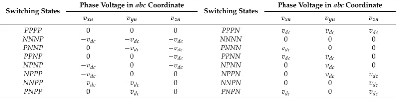
The lines to neutral voltages for all of the 16 switching vectors of a three-phase four-leg inverter
are shown in Table1. The lines to neutral voltages are transformed fromabcintoαβγcoordinates by
using Equation (17). The results of the transformation are shown in Table2.
T=
2
3 −13 −13
0 √1
3 − 1
√
3 1
3 13 13
[image:6.595.98.500.517.616.2] (17)
Table 1.The switching states with phase voltages in theabccoordinate.
Switching States Phase Voltage inabcCoordinate Switching States Phase Voltage inabcCoordinate
vxn vyn vzn vxn vyn vzn
PPPP 0 0 0 PPPN vdc vdc vdc
NNNP −vdc −vdc −vdc NNNN 0 0 0
PNNP 0 −vdc −vdc PNNN vdc 0 0
PPNP 0 0 −vdc PPNN vdc vdc 0
NPNP −vdc 0 −vdc NPNN 0 vdc 0
NPPP −vdc 0 0 NPPN 0 vdc vdc
NNPP −vdc −vdc 0 NNPN 0 0 vdc
[image:6.595.97.498.654.763.2]PNPP 0 −vdc 0 PNPN vdc 0 vdc
Table 2.The switching states with phase voltages in theαβγcoordinate.
Switching States Phase Voltage inαβγCoordinate Switching States Phase Voltage inαβγCoordinate
vα vβ vγ vα vβ vγ
PPPP 0 0 0 PPPN 0 0 vdc
NNNP 0 0 −vdc NNNN 0 0 0
PNNP 2vdc
3 0 −2v3dc PNNN 2v3dc 0
vdc
3
PPNP vdc
3
vdc √
3 −
vdc
3 PPNN v3dc
vdc √
3
2vdc
3
NPNP −vdc
3
vdc √
3 −
2vdc
3 NPNN −
vdc
3
vdc √
3
vdc
3
NPPP −2vdc
3 0 −
vdc
3 NPPN −2v3dc 0 2v3dc
NNPP −vdc
3 −
vdc √
3 −
2vdc
3 NNPN −
vdc
3 −
vdc √
3
vdc
3
PNPP vdc
3 −
vdc √
3 −
vdc
3 PNPN v3dc −
vdc √
3
2vdc
Energies2017,10, 2129 7 of 19
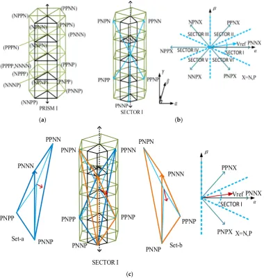
In the three-dimensional coordinate system of a three-phase four-leg inverter, there are six prisms to represent the switching voltage vectors. These prisms can be divided into six sectors (from I to
VI) such that each sector is combined with half of the two adjacent prisms, as shown in Figure2a.
The projection of the reference vector on the αβcoordinate is used to determine the sector of the
reference vector. There are six active vectors and two zeros vectors in each sector.
Table 2. The switching states with phase voltages in the αβγ coordinate.
Switching States Phase Voltage in αβγ Coordinate Switching States Phase Voltage in αβγ Coordinate
PPPP 0 0 0 PPPN 0 0
NNNP 0 0 − NNNN 0 0 0
PNNP 2
3 0 − PNNN
2
3 0 3
PPNP 3 √3 − PPNN 3 √3 23
NPNP − √3 − NPNN − √3 3
NPPP − 0 − NPPN − 0 23
NNPP − −√ − NNPN − −√ 3
PNPP 3 −√ − PNPN 3 −√ 23
In order to reduce the CMV and utilize high DC-link voltage, six active switching vectors are selected to synthesize the reference in each sector. As shown in Figure 2b, all of the sectors occupied 60° on the αβ plane, with sector I in the range of 330° to 30°, and followed by the other sectors. In order to minimize the current and harmonic content, near state switching vectors should be selected that are adjacent to the reference vector. It is seen that two prisms in each sector consist of two tetrahedrons, and there are eight switching vectors adjacent to the reference vector, four of which are selected based on the minimization of CMV and switching loss. The position of the reference vector is determined by the NSV-MPC at every sampling period. The active voltage vectors surrounding the determined reference vector are selected based on the position of the reference voltage vector. The optimal vector candidate is included among the selected voltage vectors. As shown in Figure 2c, if the reference switching vector is in sector I, four non-zero switching vectors are required to synthesize the reference vector. Therefore, two sets (Set-a and Set-b) of four switching vectors are selected in each sector. It is clear that two switching vectors (PNNP and PNNN) are chosen in both sets. Hence, there are six different switching vectors in one sector.
(a) (b)
Energies 2017, 10, 2129 8 of 20
PNNP PNN
N
PPNN PNPN
PNPP PPNP
SECTOR I
Set-b Set-a
PNPP PNNN
PPNN
PNNP
PNNP
PPNP PNNN PNPN
PNPX
PNNX PPNX
X=N,P Vref
SECTOR I
[image:7.595.109.490.166.567.2](c)
Figure 2.(a) Switching vectors and prisms (b) Projection of a sector on the αβ coordinate (c) Sector identification with near state vector selection (NSV).
The voltage vector closest to the reference voltage vector is selected by evaluating the six active vectors through the predictive model mentioned in Section 3. The optimal voltage vector is selected from the six active vectors by using the cost function in Equation (15).
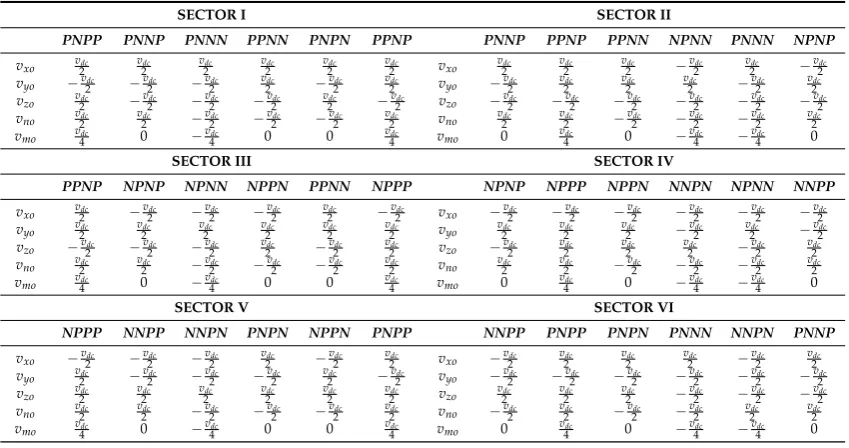
The model predictive control technique based on the near state voltage vector can be employed to find the closest voltage vector, which reduces the error between the desired and reference currents. From the predefined sectors, the proposed control method predicts the reference vector in each sampling time. Six active vectors are selected from the 14 active vectors that surround the reference vector based on the near state vectors listed in Table 3. This ensures that the CMV is confined within
± , and at the same time reduces the computational burden, as only six active vectors are used, instead of 14 vectors. However, this increases the ripple content marginally in the load current as conventional MPC. In order to overcome the problem, one zero vector—either PPPP or NNNN—can be used together with the six active vectors at each control cycle, and this causes the CMV to vary between + and− or− and + . Therefore, seven voltage vectors are selected to determine the voltage vector that is closest to the reference vector in the proposed NSV-MPC. In both cases, the computational burden is also reduced due to the reduction of switching vectors from 16 to six (considering only active vectors), and seven (including one zero vector), as shown Figure 3. As a result, NSV-MPC demonstrates the better performance with reduced computational burden. Figure 2. (a) Switching vectors and prisms (b) Projection of a sector on theαβcoordinate (c) Sector identification with near state vector selection (NSV).
In order to reduce the CMV and utilize high DC-link voltage, six active switching vectors are
selected to synthesize the reference in each sector. As shown in Figure2b, all of the sectors occupied
60◦on theαβplane, with sector I in the range of 330◦to 30◦, and followed by the other sectors. In order
to minimize the current and harmonic content, near state switching vectors should be selected that are adjacent to the reference vector. It is seen that two prisms in each sector consist of two tetrahedrons, and there are eight switching vectors adjacent to the reference vector, four of which are selected based on the minimization of CMV and switching loss. The position of the reference vector is determined by the NSV-MPC at every sampling period. The active voltage vectors surrounding the determined reference vector are selected based on the position of the reference voltage vector. The optimal vector
candidate is included among the selected voltage vectors. As shown in Figure2c, if the reference
vector. Therefore, two sets (Set-aand Set-b) of four switching vectors are selected in each sector. It is
clear that two switching vectors (PNNPandPNNN) are chosen in both sets. Hence, there are six
different switching vectors in one sector.
The voltage vector closest to the reference voltage vector is selected by evaluating the six active
vectors through the predictive model mentioned in Section3. The optimal voltage vector is selected
from the six active vectors by using the cost function in Equation (15).
The model predictive control technique based on the near state voltage vector can be employed to find the closest voltage vector, which reduces the error between the desired and reference currents. From the predefined sectors, the proposed control method predicts the reference vector in each sampling time. Six active vectors are selected from the 14 active vectors that surround the reference
vector based on the near state vectors listed in Table3. This ensures that the CMV is confined within
±vdc
4 , and at the same time reduces the computational burden, as only six active vectors are used,
instead of 14 vectors. However, this increases the ripple content marginally in the load current as
conventional MPC. In order to overcome the problem, one zero vector—eitherPPPPorNNNN—can
be used together with the six active vectors at each control cycle, and this causes the CMV to vary
between+vdc
4 and−
vdc
2 or−
vdc
4 and +
vdc
2 . Therefore, seven voltage vectors are selected to determine
the voltage vector that is closest to the reference vector in the proposed NSV-MPC. In both cases, the computational burden is also reduced due to the reduction of switching vectors from 16 to six
(considering only active vectors), and seven (including one zero vector), as shown Figure3. As a result,
[image:8.595.86.511.405.629.2]NSV-MPC demonstrates the better performance with reduced computational burden.
Table 3. Corresponding common mode voltage (CMV) based on the near state vector (NSV) of each sector.
SECTOR I SECTOR II
PNPP PNNP PNNN PPNN PNPN PPNP PNNP PPNP PPNN NPNN PNNN NPNP
vxo v2dc
vdc 2 vdc 2 vdc 2 vdc 2 vdc
2 vxo v2dc
vdc 2 vdc 2 − vdc 2 vdc 2 − vdc 2
vyo −v2dc −
vdc 2 − vdc 2 vdc 2 − vdc 2 vdc
2 vyo −v2dc
vdc 2 vdc 2 vdc 2 − vdc 2 vdc 2
vzo v2dc −v2dc −v2dc −v2dc v2dc −v2dc vzo −v2dc −v2dc −v2dc −v2dc −v2dc −v2dc
vno v2dc v2dc −v2dc −v2dc −v2dc v2dc vno v2dc v2dc −v2dc −v2dc −v2dc v2dc
vmo v4dc 0 −v4dc 0 0 v4dc vmo 0 v4dc 0 −v4dc −v4dc 0
SECTOR III SECTOR IV
PPNP NPNP NPNN NPPN PPNN NPPP NPNP NPPP NPPN NNPN NPNN NNPP
vxo v2dc −v2dc −v2dc −v2dc v2dc −v2dc vxo −v2dc −v2dc −v2dc −v2dc −v2dc −v2dc
vyo v2dc
vdc 2 vdc 2 vdc 2 vdc 2 vdc
2 vyo v2dc
vdc 2 vdc 2 − vdc 2 vdc 2 − vdc 2
vzo −v2dc −
vdc 2 − vdc 2 vdc 2 − vdc 2 vdc
2 vzo −v2dc
vdc 2 vdc 2 vdc 2 − vdc 2 vdc 2
vno v2dc
vdc 2 − vdc 2 − vdc 2 − vdc 2 vdc
2 vno v2dc
vdc 2 − vdc 2 − vdc 2 − vdc 2 vdc 2
vmo v4dc 0 −v4dc 0 0 v4dc vmo 0 v4dc 0 −v4dc −v4dc 0
SECTOR V SECTOR VI
NPPP NNPP NNPN PNPN NPPN PNPP NNPP PNPP PNPN PNNN NNPN PNNP
vxo −v2dc −v2dc −v2dc v2dc −v2dc v2dc vxo −v2dc v2dc v2dc v2dc −v2dc v2dc
vyo v2dc −v2dc −v2dc −v2dc v2dc −v2dc vyo −v2dc −v2dc −v2dc −v2dc −v2dc −v2dc
vzo v2dc
vdc 2 vdc 2 vdc 2 vdc 2 vdc
2 vzo v2dc
vdc 2 vdc 2 − vdc 2 − vdc 2 − vdc 2
vno v2dc
vdc 2 − vdc 2 − vdc 2 − vdc 2 vdc
2 vno −v2dc
vdc 2 − vdc 2 − vdc 2 vdc 2 vdc 2
vmo v4dc 0 −
vdc
4 0 0
vdc
4 vmo 0 v4dc 0 −
vdc
4 −
vdc
4 0
A step-by-step implementation procedure for NSV-MPC is summarized below:
Step 1. Measure the load currents i(k) and calculate the reference currents i*(k + 1) by using
Equation (13)
Step 2. Identify the sector on theαβplane in theαβγcoordinate and the corresponding voltage vectors
at every sampling period.
Step 3. Predict the future voltage vector for all of the possible switching states from the identified
sector from Table3.
Step 4. Predict the load currentsi(k+ 1) of all of the possible switching states from the identified sector
Step 5. Evaluate the cost functiong(k+ 1) by using Equation (16). Step 6. 7Select the switching state that optimizes the cost function.
Step 7. 7Apply the selected switching action to fire the inverter switches.Energies 2017, 10, 2129 9 of 20
m
R
fxR
fyR
fzR
fn LfxL
fyL
fzL
fnR
xR
yR
z VoltageVector Selection
Future Current Prediction Model
Cost Function Optimization
for selecting optimal voltage vector Measured Current
6/7
Reference Current
Main loop
S
xS
yS
zS
nvdc
i*
(k
+
1
)
v(k+1) i(k)
i(
k+
1
)
In
ver
ter
The sector determination using projection on the αβ
plane
Transformation abc to αβγ
Extrapolation i*(k)
[image:9.595.110.485.148.306.2]Sine Wave Generator using LabVIEW FPGA
Figure 3. Proposed near state vector selection-based model predictive control (NSV-MPC) block diagram.
Table 3. Corresponding common mode voltage (CMV) based on the near state vector (NSV) of each sector.
SECTOR I SECTOR II
PNPP PNNP PNNN PPNN PNPN PPNP PNNP PPNP PPNN NPNN PNNN NPNP
− −
− − − − − −
− − − − − − − − − −
− − − − − −
0 − 0 0 0 0 − − 0
SECTOR III SECTOR IV
PPNP NPNP NPNN NPPN PPNN NPPP NPNP NPPP NPPN NNPN NPNN NNPP
− − − − − − − − − −
− −
− − − − − −
− − − − − −
0 − 0 0 0 0 − − 0
SECTOR V SECTOR VI
NPPP NNPP NNPN PNPN NPPN PNPP NNPP PNPP PNPN PNNN NNPN PNNP
− − − − − −
− − − − − − − − − −
− − −
− − − − − −
[image:9.595.163.434.480.613.2]0 − 0 0 0 0 − − 0
Figure 3.Proposed near state vector selection-based model predictive control (NSV-MPC) block diagram.
5. Simulation and Experimental Results
The proposed NSV-MPC has been validated in simulation by using Matlab/Simulink. Then, it is also validated through experimental implementation with a three-phase four-leg inverter laboratory
prototype. The parameters of the inverter are as specified in Table 4. The experimental test was
carried out using a field programmable gate array (FPGA)-based controller, and it can be used to implement the parallel processing technique of the model predictive controller to enhance the system dynamic response.
Table 4.Parameters of the experimental results.
Variable Parameter Value
vdc DC-link voltage 320 V
C DC-link capacitance 2.2 mF
Lf Filter inductance 15 mH
Ts Sampling time 50µs
R Load resistance 12Ω
Rf Filter resistance 0.1Ω
f* Reference nominal frequency 50 Hz
i* Reference nominal peak current 10 A
Lfn Neutral-leg inductance 8 mH
fs Sampling frequency kHz
5.1. Experimental Setup
The current references were read by the NI LabVIEW FPGA 2015 module, which connected to a
host computer. Figure4depicts the project setup in the laboratory. A National Instrument Single-Board
Energies 2017, 10, 2129 11 of 20
Power Analyzer
Inverter
Oscilloscope
Gate driver
DC Source Resistive Load
Inductive Load
Laptop GPIC Board Current and
[image:10.595.101.496.89.318.2]Voltage Sensor
Figure 4. Experimental setup in the FPGA platform.
5.2. Results and Performance Analysis
All of the experimental results in this section were obtained by using the weighting factor
= 0.5 and sampling time = 50 μs. The same experimental validation was carried out for both conventional MPC and NSV-MPC. Ideally, the DC-link capacitors of a two-level four-leg inverter share equal voltages due to utilizing the full DC-link voltage by adopting the switching scheme. Three cases were considered in this work:
Case 1. All available voltage vectors in conventional MPC at every sampling time.
Case 2. One zero vector—either PPPP or NNNN—with six active vectors in proposed NSV-MPC at every sampling time.
Case 3. Six active vectors in proposed NSV-MPC at every sampling time.
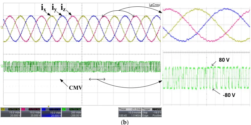
In the first case, a conventional MPC utilized 16 switching vectors to predict the future reference vector in each control cycle. Hence, the CMV was high, and required a large computational burden due to the high calculation time required to select the desire voltage vector. The peak value of CMV oscillated between – and + due to the alternating use of two zero vectors in the control algorithm, as illustrated in Figure 5.
15 10 5 0 -5 -10 -15 200 100 0 -100 -200
0.01
0 0.02 0.03 0.04 0.05 0.06 0.07 0.08 0.09 0.1 15 10 5 0 -5 -10 -15 200 100 0 -100 -200
Vo
lt
ag
e
(
v)
Cu
rr
e
n
t (
A
)
[image:10.595.94.504.593.733.2](a)
Figure 4.Experimental setup in the FPGA platform.
5.2. Results and Performance Analysis
All of the experimental results in this section were obtained by using the weighting factor
wswc=0.5 and sampling timeTs=50µs. The same experimental validation was carried out for both
conventional MPC and NSV-MPC. Ideally, the DC-link capacitors of a two-level four-leg inverter share equal voltages due to utilizing the full DC-link voltage by adopting the switching scheme. Three cases were considered in this work:
Case 1. All available voltage vectors in conventional MPC at every sampling time.
Case 2. One zero vector—eitherPPPPorNNNN—with six active vectors in proposed NSV-MPC at
every sampling time.
Case 3. Six active vectors in proposed NSV-MPC at every sampling time.
In the first case, a conventional MPC utilized 16 switching vectors to predict the future reference vector in each control cycle. Hence, the CMV was high, and required a large computational burden due to the high calculation time required to select the desire voltage vector. The peak value of CMV
oscillated between−vdc
2 and +
vdc
2 due to the alternating use of two zero vectors in the control algorithm,
as illustrated in Figure5. Power Analyzer
Inverter
Oscilloscope
Gate driver
DC Source Resistive Load
Inductive Load
Laptop
GPIC Board Current and
Voltage Sensor
Figure 4. Experimental setup in the FPGA platform.
5.2. Results and Performance Analysis
All of the experimental results in this section were obtained by using the weighting factor
= 0.5 and sampling time = 50 μs. The same experimental validation was carried out for both conventional MPC and NSV-MPC. Ideally, the DC-link capacitors of a two-level four-leg inverter share equal voltages due to utilizing the full DC-link voltage by adopting the switching scheme. Three cases were considered in this work:
Case 1. All available voltage vectors in conventional MPC at every sampling time.
Case 2. One zero vector—either PPPP or NNNN—with six active vectors in proposed NSV-MPC at every sampling time.
Case 3. Six active vectors in proposed NSV-MPC at every sampling time.
In the first case, a conventional MPC utilized 16 switching vectors to predict the future reference vector in each control cycle. Hence, the CMV was high, and required a large computational burden due to the high calculation time required to select the desire voltage vector. The peak value of CMV oscillated between – and + due to the alternating use of two zero vectors in the control algorithm, as illustrated in Figure 5.
15 10 5 0 -5 -10 -15
200
100
0
-100
-200 0.01
0 0.02 0.03 0.04 0.05 0.06 0.07 0.08 0.09 0.1 15 10 5 0 -5 -10 -15
200
100
0
-100
-200
Vo
lt
ag
e
(
v)
Cu
rr
e
n
t (
A
)
(a)
ix iy iz
CMV
-160 V 160 V
[image:11.595.101.497.88.231.2](b)
Figure 5. Each phase current and common mode voltage (CMV) for Case 1 (a) Simulation result, (b) Experimental result (I = 10 A/div. CMV = 200 V/div. and 10 ms/div.).
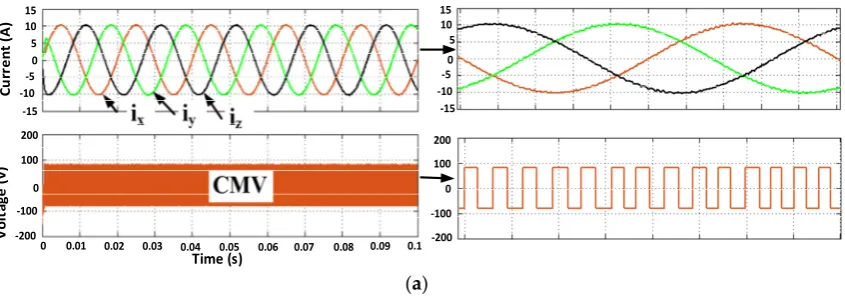
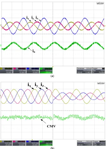
In the second case, the NSV−MPC scheme utilized only one zero vector—either PPPP or NNNN—together with six active vectors at every sampling time. As shown in Figure 6, the one-sided peak value of CMV is large, and varies between and − or between − and respectively, due to the use of one zero vector. The computational burden is reduced since the number of switching voltage vectors is reduced.
15 10 5 0 -5 -10 -15
200
100
0
-100
-200 0.01
0 0.02 0.03 0.04 0.05 0.06 0.07 0.08 0.09 0.1 15 10 5 0 -5 -10 -15
200
100
0
-100
-200
Vo
lt
ag
e (
v)
Cu
rr
e
n
t (
A
)
Time (s)
(a)
i
xi
yi
zCMV
-160 V 80 V
[image:11.595.102.489.363.672.2](b)
Figure 5.Each phase current and common mode voltage (CMV) for Case 1 (a) Simulation result, (b) Experimental result (I= 10 A/div. CMV = 200 V/div. and 10 ms/div.).
In the second case, the NSV−MPC scheme utilized only one zero vector—either PPPP or
NNNN—together with six active vectors at every sampling time. As shown in Figure6, the one-sided
peak value of CMV is large, and varies between vdc
4 and−
vdc
2 or between−
vdc
4 and
vdc
2 respectively,
due to the use of one zero vector. The computational burden is reduced since the number of switching voltage vectors is reduced.
Energies 2017, 10, 2129 12 of 20
ix iy iz
CMV
-160 V 160 V
(b)
Figure 5. Each phase current and common mode voltage (CMV) for Case 1 (a) Simulation result, (b) Experimental result (I = 10 A/div. CMV = 200 V/div. and 10 ms/div.).
In the second case, the NSV−MPC scheme utilized only one zero vector—either PPPP or NNNN—together with six active vectors at every sampling time. As shown in Figure 6, the one-sided peak value of CMV is large, and varies between and − or between − and respectively, due to the use of one zero vector. The computational burden is reduced since the number of switching voltage vectors is reduced.
15 10 5 0 -5 -10 -15 200 100 0 -100 -200
0.01
0 0.02 0.03 0.04 0.05 0.06 0.07 0.08 0.09 0.1 15 10 5 0 -5 -10 -15 200 100 0 -100 -200
Vo
lt
ag
e (
v)
Cu
rr
e
n
t (
A
)
Time (s)
(a)
i
xi
yi
zCMV
-160 V 80 V
(b)
EnergiesEnergies 2017,201710, 2129, 10, 2129 13 of 20 12 of 19 15 10 5 0 -5 -10 -15 200 100 0 -100 -200 0.01
0 0.02 0.03 0.04 0.05 0.06 0.07 0.08 0.09 0.1 15 10 5 0 -5 -10 -15 200 100 0 -100 -200 Vo lt a g e ( v ) Cu rr e n t ( A ) Time (s)
(c)
ix
iy
iz
CMV
-80 V 160 V
[image:12.595.111.484.86.389.2](d)
Figure 6.Each phase current and CMV for Case 2, first considering PPPP as the switching state: (a) Simulation result, (b) Experimental result; and considering NNNN as the switching state (c) Simulation result, (d) Experimental result (I = 10 A/div., CMV = 200 V/div. and 10 ms/div.).
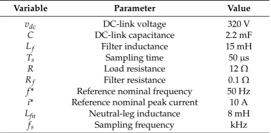
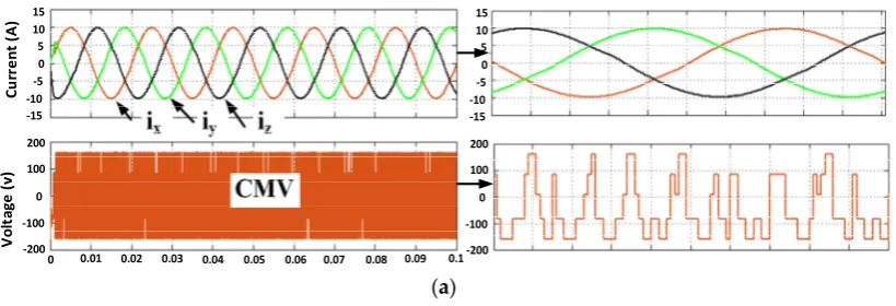
In the third case, the proposed NSV-MPC was applied by using only six active vectors in each sampling instant to significantly reduce the peak-to-peak value of the CMV. Consequently, the calculation burden is also reduced through using a reduced number of switching vectors. Even though the ripple content in the load current is marginally higher than in Case 2, it is still in an allowable range. The CMV is confined within ± , as shown in Figure 7.
15 10 5 0 -5 -10 -15 200 100 0 -100 -200 0.01
0 0.02 0.03 0.04 0.05 0.06 0.07 0.08 0.09 0.1 10 5 0 -5 -10 -15 200 100 0 -100 -200 15 Vo lt ag e ( v) Cu rr e n t ( A ) Time (s)
[image:12.595.88.511.535.688.2](a)
Figure 6.Each phase current and CMV for Case 2, first consideringPPPPas the switching state: (a) Simulation result, (b) Experimental result; and consideringNNNNas the switching state (c) Simulation result, (d) Experimental result (I= 10 A/div., CMV = 200 V/div. and 10 ms/div.).
In the third case, the proposed NSV-MPC was applied by using only six active vectors in each sampling instant to significantly reduce the peak-to-peak value of the CMV. Consequently, the calculation burden is also reduced through using a reduced number of switching vectors. Even though the ripple content in the load current is marginally higher than in Case 2, it is still
in an allowable range. The CMV is confined within±vdc
4 , as shown in Figure7.
15 10 5 0 -5 -10 -15 200 100 0 -100 -200 0.01
0 0.02 0.03 0.04 0.05 0.06 0.07 0.08 0.09 0.1 15 10 5 0 -5 -10 -15 200 100 0 -100 -200 Vo lt a g e ( v ) Cu rr e n t ( A ) Time (s)
(c)
ix
iy
iz
CMV
-80 V 160 V
(d)
Figure 6.Each phase current and CMV for Case 2, first considering PPPP as the switching state: (a) Simulation result, (b) Experimental result; and considering NNNN as the switching state (c) Simulation result, (d) Experimental result (I = 10 A/div., CMV = 200 V/div. and 10 ms/div.).
In the third case, the proposed NSV-MPC was applied by using only six active vectors in each sampling instant to significantly reduce the peak-to-peak value of the CMV. Consequently, the calculation burden is also reduced through using a reduced number of switching vectors. Even though the ripple content in the load current is marginally higher than in Case 2, it is still in an allowable range. The CMV is confined within ± , as shown in Figure 7.
15 10 5 0 -5 -10 -15 200 100 0 -100 -200 0.01
0 0.02 0.03 0.04 0.05 0.06 0.07 0.08 0.09 0.1 10 5 0 -5 -10 -15 200 100 0 -100 -200 15 Vo lt ag e ( v) Cu rr e n t ( A ) Time (s)
(a)
i
xi
yi
zCMV
-80 V 80 V
[image:13.595.92.504.86.291.2](b)
Figure 7. Each phase current and CMV for Case 3 (a) Simulation result, (b) Experimental result (I = 10 A/div., CMV = 200 V/div. and 10 ms/div.).
[image:13.595.108.487.414.706.2]The Fast Fourier Transform (FFT) analysis of CMV was obtained using the powergui/FFT Analysis Toolbox of Matlab/Simulink software. The results of the mentioned cases are illustrated in Figure 8. As shown in the figures, the CMVs of the proposed NSV-MPC are significantly reduced as compared with the conventional MPC, which is due to the reduced number of voltage vectors in NSV-MPC.
0 10 20 30 40 50 Frequency (kHz) 40 0 10 20 30 Ma gn itu de (V )
0 10 20 30 40 50
Frequency (kHz) 0 5 10 15 20 25 30 35 40 M agn it ud e ( V )
(a) (b)
0 10 20 30 40 50
Frequency (kHz) 0 5 10 15 20 25 30 35 M agn it ud e ( V )
(c)
0 10 20 30 40 50
Frequency (kHz) 0 10 20 30 40 50 M agn it ud e ( V )
(d)
Figure 8. FFT analysis results of CMV (a) Conventional MPC, (b) Proposed NSV-MPC with PPPP vector, (c) Proposed NSV-MPC with NNNN vector, (d) Proposed NSV-MPC with active vectors only.
Figure 7. Each phase current and CMV for Case 3 (a) Simulation result, (b) Experimental result (I= 10 A/div., CMV = 200 V/div. and 10 ms/div.).
The Fast Fourier Transform (FFT) analysis of CMV was obtained using the powergui/FFT Analysis
Toolbox of Matlab/Simulink software. The results of the mentioned cases are illustrated in Figure8.
As shown in the figures, the CMVs of the proposed NSV-MPC are significantly reduced as compared with the conventional MPC, which is due to the reduced number of voltage vectors in NSV-MPC.
Energies 2017, 10, 2129 14 of 20
i
xi
yi
zCMV
-80 V 80 V
(b)
Figure 7. Each phase current and CMV for Case 3 (a) Simulation result, (b) Experimental result (I = 10 A/div., CMV = 200 V/div. and 10 ms/div.).
The Fast Fourier Transform (FFT) analysis of CMV was obtained using the powergui/FFT Analysis Toolbox of Matlab/Simulink software. The results of the mentioned cases are illustrated in Figure 8. As shown in the figures, the CMVs of the proposed NSV-MPC are significantly reduced as compared with the conventional MPC, which is due to the reduced number of voltage vectors in NSV-MPC.
0 10 20 30 40 50 Frequency (kHz) 40 0 10 20 30 Ma gn itu de (V )
0 10 20 30 40 50 Frequency (kHz) 0 5 10 15 20 25 30 35 40 M agn it ud e ( V )
(a) (b)
0 10 20 30 40 50 Frequency (kHz) 0 5 10 15 20 25 30 35 M agn it ud e ( V )
(c)
0 10 20 30 40 50 Frequency (kHz) 0 10 20 30 40 50 M agn it ud e ( V )
(d)
Figure9illustrates the unbalanced loading condition and the transient analysis of the proposed
NSV-MPC method with balanced loads and filters. Figure9a represents the unbalanced references
connected to the balanced load and filter parameters. The unbalanced current flow in the fourth leg is known as the zero-sequence current, which is detected by adding the vectors of three phase currents.
Figure9b shows the response of a step change in phase -yand -zreferences from 10 A to 5 A. During
the transient instant, the inverter load currents tracked their corresponding reference very well for the step change condition. In these cases, NSV-MPC showed the fast-dynamic response during the transient state.
Figure 9 illustrates the unbalanced loading condition and the transient analysis of the proposed NSV-MPC method with balanced loads and filters. Figure 9a represents the unbalanced references connected to the balanced load and filter parameters. The unbalanced current flow in the fourth leg is known as the zero-sequence current, which is detected by adding the vectors of three phase currents. Figure 9b shows the response of a step change in phase -y and -z references from 10 A to 5 A. During the transient instant, the inverter load currents tracked their corresponding reference very well for the step change condition. In these cases, NSV-MPC showed the fast-dynamic response during the transient state.
i
xi
yi
zi
n(a)
i
x
i
y
i
z
CMV
(b)
Figure 9. (a) Unbalanced references in phase -y and -z from 10 A to 5A with balanced resistive loads and filters, and (b) Step change in phase -y and -z references from 10 A to 5A with the proposed NSV-MPC technique.
6. Robustness Analysis and Performance Evaluation
[image:14.595.121.479.204.708.2]6. Robustness Analysis and Performance Evaluation
The performance and robustness analyses of the proposed control scheme are performed in the following section.
6.1. Robustness Analysis of Model Parameter Variations
The controller accuracy depends on the system parameters and the discrete predictive model. The effectiveness of the NSV-MPC was tested through robustness analysis by varying the system parameters. The response of the proposed system against the inductive filter variation was validated through both simulation and an experiment. Two cases were carried out: (a) CF: Change in inductive filter but no change in controller, where the filter’s inductance changed from 6 mH to 18 mH without providing the information of the filter changes to the controller. (b) CCF: Changes to both the filter as well as to the controller, where the changed filter values are given to the controller to evaluate the
effectiveness. In Figure10a, the percentages of total harmonic distortion (THD) with respect to the
variation of inductive value have been shown.
Energies 2017, 10, 2129 16 of 20
The performance and robustness analyses of the proposed control scheme are performed in the following section.
6.1. Robustness Analysis of Model Parameter Variations
The controller accuracy depends on the system parameters and the discrete predictive model. The effectiveness of the NSV-MPC was tested through robustness analysis by varying the system parameters. The response of the proposed system against the inductive filter variation was validated through both simulation and an experiment. Two cases were carried out: (a) CF: Change in inductive filter but no change in controller, where the filter’s inductance changed from 6 mH to 18 mH without providing the information of the filter changes to the controller. (b) CCF: Changes to both the filter as well as to the controller, where the changed filter values are given to the controller to evaluate the effectiveness. In Figure 10a, the percentages of total harmonic distortion (THD) with respect to the variation of inductive value have been shown.
(a)
R
ef
ere
nce a
nd
Mea
su
red
C
urre
nt
s (A
)
Time (Seconds)
i
yi
z
i
xi
xi
yi
z(b) 0
2 4 6 8 10 12 14
[image:15.595.131.467.295.746.2]6 mH 9 mH 12 mH 15 mH 18 mH
C
ur
ren
t t
ra
ck
in
g
err
or
(A
)
[image:16.595.169.430.89.278.2]Sample =2001 (c)
Figure 10.The results of proposed NSV-MPC: (a) The percentages of THD with respect to variation in inductive value, (b) Reference and measured currents, (c) Current tracking error of phase x.
6.2. Reference Current Tracking Error
Each leg of the three-phase four-leg inverter generated an independent voltage to control the zero-sequence voltage or current. The reference current tracking error of the proposed control scheme is very accurate. Figure 10b shows the reference and measured currents, and Figure 10c shows that the tracking error of current ( ∗( ) − ( )) in phase x is confined within ±0.82 A. The percentage of reference tracking error with respect to the load current can be calculated from the reference and load current as follows:
[image:16.595.89.506.683.764.2]_ (%) =
1 ∑ |∗( ) − ( )|
( ) (18)
where b = x, y, z and a = 2001 is the number of samples used in simulation.
The peak-to-peak value of CMV, THD (%) of load current, and execution time of the proposed system were collected to assess the performance of the system. The proposed NSV-MPC technique improved the processing time by reducing the computational burden through using fewer numbers of voltage vectors in every control cycle. The number of ticks (1 tick = 25 ns) required by the proposed controller in completing each iteration of the control loop with a LabVIEW FPGA-based platform was less than the conventional controller. The comparisons of NSV-MPC and conventional MPC are illustrated in Tables 5 and 6.
Table 5. Execution time measurement.
Strategy Conventional MPC Execution Time (tick)
Proposed NSV-MPC Execution Time (tick)
Improvement
(1 tick = 25 ns) (1 tick = 25 ns) (%)
No. of Switching Vectors 16 336 6 187 44.34
7 201 40.17
Table 6. CMV, percentage of THD, and current tracking error variation at different sampling times.
Strategy CMV
Variation
THD
(%)
Current Tracking
Error (%)
THD
(%)
Current Tracking
Error (%)
THD
(%)
Current Tracking
Error (%)
Sampling Frequency Sampling Frequency Sampling Frequency
50 kHz 20 kHz 10 kHz
Conventional MPC −160 to 160 3.47% 3.58% 3.90% 4.68% 6.65% 6.59% NSV-MPC with
PPPP vector −160 to 80 3.24% 3.36% 3.83% 4.26% 6.34% 6.11% Figure 10.The results of proposed NSV-MPC: (a) The percentages of THD with respect to variation in inductive value, (b) Reference and measured currents, (c) Current tracking error of phasex.
6.2. Reference Current Tracking Error
Each leg of the three-phase four-leg inverter generated an independent voltage to control the zero-sequence voltage or current. The reference current tracking error of the proposed control scheme
is very accurate. Figure10b shows the reference and measured currents, and Figure10c shows that
the tracking error of current (i∗x(k)−ix(k)) in phasexis confined within±0.82 A. The percentage of reference tracking error with respect to the load current can be calculated from the reference and load current as follows:
ierror_b(%) =
1
a∑ka|i∗b(k)−ib(k)|
ib(k)rms
(18)
whereb=x,y,zanda= 2001 is the number of samples used in simulation.
The peak-to-peak value of CMV, THD (%) of load current, and execution time of the proposed system were collected to assess the performance of the system. The proposed NSV-MPC technique improved the processing time by reducing the computational burden through using fewer numbers of voltage vectors in every control cycle. The number of ticks (1 tick = 25 ns) required by the proposed controller in completing each iteration of the control loop with a LabVIEW FPGA-based platform was less than the conventional controller. The comparisons of NSV-MPC and conventional MPC are
illustrated in Tables5and6.
Table 5.Execution time measurement.
Strategy Conventional MPC Execution
Time (tick)
Proposed NSV-MPC Execution
Time (tick)
Improvement
(1 tick = 25 ns) (1 tick = 25 ns) (%)
No. of Switching Vectors 16 336 67 187201 44.3440.17
Table 6.CMV, percentage of THD, and current tracking error variation at different sampling times.
Strategy CMV
Variation
THD (%)
Current Tracking Error (%)
THD (%)
Current Tracking Error (%)
THD (%)
Current Tracking Error (%)
Sampling Frequency Sampling Frequency Sampling Frequency
50 kHz 20 kHz 10 kHz
Conventional MPC −160 to 160 3.47% 3.58% 3.90% 4.68% 6.65% 6.59%
NSV-MPC with
Table 6.Cont.
Strategy CMV
Variation
THD (%)
Current Tracking Error (%)
THD (%)
Current Tracking Error (%)
THD (%)
Current Tracking Error (%)
Sampling Frequency Sampling Frequency Sampling Frequency
50 kHz 20 kHz 10 kHz
NSV-MPC with
NNNNvector −80 to 160 3.24% 3.36% 3.83% 4.26% 6.33% 6.13%
NSV-MPC with
active vectors −80 to 80 3.62% 3.22% 4.37% 4.05% 6.58% 5.87%
7. Conclusions
In this paper, the NSV-MPC method was proposed to mitigate CMV as well as reduce computational burden. The proposed NSV-MPC method determined the active vectors based on the
reference vector position, and was able to confine CMV within±vdc
4 . Moreover, this control technique
reduced the computational burden by using a minimum number of usable voltage vectors in every sampling period. The experimental results for all of the possible combinations of switching vector selection were demonstrated to show the effectiveness of the proposed control method as compared with the conventional model predictive control. Besides, the load currents were able to track their references accurately. The steady state and transient state response showed the robustness and the effectiveness of the proposed control method.
Author Contributions: Abdul Mannan Dadu has contributed to the theoretical analysis, simulation and experimental verification, and preparing the article; Saad Mekhilef has contributed to preparing the article; Tey Kok Soon, Mehdi Seyedmahmoudian and Ben Horan has contributed to the theoretical analysis and preparing the article.
Conflicts of Interest:The authors declare no conflict of interest.
References
1. Philip, J.; Jain, C.; Kant, K.; Singh, B.; Mishra, S.; Chandra, A.; Al-Haddad, K. Control and Implementation of a Standalone Solar Photovoltaic Hybrid System.IEEE Trans. Ind. Appl.2016,52, 3472–3479. [CrossRef] 2. Pichan, M.; Rastegar, H. Sliding Mode Control of Four-Leg Inverter with Fixed Switching Frequency for
Uninterruptible Power Supply Applications.IEEE Trans. Ind. Electron.2017,64, 6805–6814. [CrossRef] 3. Rodriguez, C.T.; Fuente, D.V.D.L.; Garcera, G.; Figueres, E.; Moreno, J.A.G. Reconfigurable Control Scheme
for a PV Microinverter Working in Both Grid-Connected and Island Modes.IEEE Trans. Ind. Electron.2013, 60, 1582–1595. [CrossRef]
4. Singh, B.; Sharma, S. Design and Implementation of Four-Leg Voltage-Source-Converter-Based VFC for Autonomous Wind Energy Conversion System.IEEE Trans. Ind. Electron.2012,59, 4694–4703. [CrossRef] 5. Liang, J.; Green, T.C.; Feng, C.; Weiss, G. Increasing Voltage Utilization in Split-Link, Four-Wire Inverters.
IEEE Trans. Power Electron.2009,24, 1562–1569. [CrossRef]
6. Karanki, S.B.; Geddada, N.; Mishra, M.K.; Kumar, B.K. A Modified Three-Phase Four-Wire UPQC Topology With Reduced DC-Link Voltage Rating.IEEE Trans. Ind. Electron.2013,60, 3555–3566. [CrossRef]
7. Kim, J.-H.; Sul, S.-K. A carrier-based PWM method for three-phase four-leg voltage source converters. IEEE Trans. Power Electron.2004,19, 66–75. [CrossRef]
8. Yaramasu, V.; Rivera, M.; Narimani, M.; Bin, W.; Rodriguez, J. Model Predictive Approach for a Simple and Effective Load Voltage Control of Four-Leg Inverter With an Output Filter.IEEE Trans. Ind. Electron.2014,61, 5259–5270. [CrossRef]
9. Rivera, M.; Yaramasu, V.; Rodriguez, J.; Bin, W. Model Predictive Current Control of Two-Level Four-Leg Inverters Part II: Experimental Implementation and Validation. IEEE Trans. Power Electron. 2013, 28, 3469–3478. [CrossRef]