International Journal of Emerging Technology and Advanced Engineering
Website: www.ijetae.com (ISSN 2250-2459,ISO 9001:2008 Certified Journal, Volume 4, Issue 8, August 2014)
554
Low-voltage Power-efficient Dynamic Latched Comparator
Surya Kant
1, Bhavana P. Shrivastava
2 1Student, MANIT, Bhopal 2Assistant Professor, ECE Department MANIT, Bhopal
Abstract—A new dynamic comparator is presented using modified gain stage followed by latch stage for high speed analog-to-digital converter. The gain stage of proposed comparator is a modified class AB pre-amplifier which makes it suitable for high speed of operation with small delay time and low power. The circuit is simulated in 180 nm process technology using tool Cadence Virtuoso with a supply voltage of 1.2V operating at maximum sampling frequency of 2 GHz. After simulation the circuit results shows that it has 323.0 pS delay time and 38.99 µW power for common mode voltage Vcm = 0.7 , input differential voltage (∆Vin = 1 mV) operating at sampling frequency of 500 MHz at 1.2 V supply voltage. Simulation results confirms that the proposed comparator considerably reduces the delay and power consumption
Keywords— Analog-to-digital convertor (ADC), sense amplifier (SA), pre-amplifier, Latched comparator, Low voltage, Clock sampling frequency.
I. INTRODUCTION
In present world, requirement of portable battery operated devices is increasing. For portable devices, there is a huge requirement of low power consumption and high speed circuits. This can be achieved by using microelectronics devices and scaling its size.
Now a days, analog signals are processed in digital domain hence analogue to digital convertor (ADCs) and digital to analog convertor (DACs) are useful component of digital instruments. Comparator is one of the most useful and fundamental building block in most analogue to digital converters (ADCs). Due to high-speed, low-power consumption, dynamic latched comparator are very attractive in designing of flash ADCs, sense amplifier (SAs), data transmission, switching power regulators and others.
Dynamic latched comparators have one or two stages of pre-amplification followed by track-and-latch stage. In track-and-latch stage positive feedback mechanism is used with back-to-back cross-coupled inverter (latch) to amplify the analog signal further into a full scale digital level. However, the accuracy of latched comparator is limited by an input-referred offset voltage, resulting from the device
mismatch such as current factor (β = µCox ), threshold voltage (Vth) and capacitance mismatch [4], [5]. Because of this, the input-referred offset voltage is very important design parameter. A less mismatch can be achieved by using large devices resulting more delay and the more power consumption.
This paper is organized as follow. Section II describe some dynamic latched comparators along with their working principle, delay calculation and their limitations. Section III introduces proposed
II. DYNAMIC LATCHED COMPARATOR
International Journal of Emerging Technology and Advanced Engineering
Website: www.ijetae.com (ISSN 2250-2459,ISO 9001:2008 Certified Journal, Volume 4, Issue 8, August 2014)
555
M1
M2 M3
M4 M5
M6 M7
M8 M9
M10 M11
M12 VDD
Clk
Clk
VinP VinN
Np
Clkb
VoutP
VoutN
Nn
IL1 IL2
Ilatch
Ibias
[image:2.612.77.261.135.441.2]IB1 IB2
Figure 1. Double-tail latch-type voltage SA.
A. Double-tail latch-type voltage SA
Figure.1 shows schematic of double-tail latch-type voltage sense amplifier [10]. For its operation, during reset phase (Clk=0, Clkb = VDD), transistors M4 and M5 turn on and the Np and Nn node capacitances are pre-charge to VDD through transistors. The output at node Np and Nn are input to the transistors M10 and M11 turning them on. The VoutP and VoutN discharges to ground thorough transistors M10 and M11 during reset phase. During evaluation phase when Clk = VDD, input stage tail transistor M1 turn on and input transistor M2 and M3 starts discharging Np and Nn node from VDD to ground generating input dependent differential mode voltage. This differential mode voltage pass to cross-coupled latch stage through transistor M10 and M11. The latch stage reestablish the Nn and Np node voltage difference to make one of the output node voltage (Vout) high. M10 and M11 provide isolation between input and output by separating input stage and out cross-coupled stage which reduces kickback noise [6]. The differential node voltage totally depends on the transconductance (gm) of input transistor.
[image:2.612.325.565.165.282.2]To get high gain, the size of input transistor should be large which increases the power dissipation.
Figure 2. Transient waveform.
1) Delay Calculation:
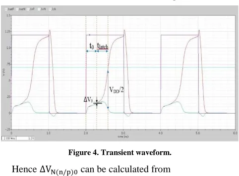
Suppose VinP>VinN then delay of latched comparator mainly depends upon two delay time as shown in Figure 2.
1. Charge time (t0): time it takes to charge the load capacitance (CLout) of latch stage to turn on latch regeneration. The latch stage starts regeneration when M6/M7 turns on hence VoutP/VoutN should charge up to Vtn. The charge time t0 is given by [7, 17].
. (1)
Where CL is output capacitance of latch, IL1 is drain current of M8 and Ilatch is current through M12. And IL1 = IL2 = Ilatch/2 for small differential Np/Nn node voltage ∆VNp/Nn..
2. Latch delay (tlatch): time latch stage takes to give differential output half of the full voltage swing (VDD). Therefore, latch delay can be given by [7, 17]
(
) (
⁄
) (2)
Where gm,eff is transconductance of each inverter of latch stage and ∆V0 is output difference voltage at time t = t0 which is calculated from equation (3).
| ( ) ( )|
| | | | (
)
| | (
) (3)
Where IL1 and IL2 are current flowing through each inverter of the latch as shown in Figure 1. Let
[image:2.612.363.557.584.652.2]International Journal of Emerging Technology and Advanced Engineering
Website: www.ijetae.com (ISSN 2250-2459,ISO 9001:2008 Certified Journal, Volume 4, Issue 8, August 2014)
556
Where gm10 = gm11 are transconductance of M10 and M11 and ∆VNn/Np is voltage difference of node Nn and Np of first stage. From equations (3) and (4) ∆V0 can be given as
⁄ (5)
∆VNn/Np are feed to intermediate stage transistor M10 and M11 which imbalance the latch to start regeneration. Hence from equation (5) it is clear that ∆V0 is proportional to ∆VNn/Np. Higher the value of ∆VNn/Np faster will be the regeneration speed. The differential node voltage of Nn/Np can be calculated as
⁄ | ( ) ( )|
(6)
Where IB1 and IB2 are current through M2 and M3 gm2 is transconductance of M2 which is equal to transconductance of M3. CL,N is output capacitance of node Nn/Np. From equations (5) and (6) ∆V0 can be given as
⁄
(
) (7)
From equations (1) (2) and (7) the total delay of this comparator can be given as
( ⁄
)
(
) (8)
From equation (8) it is clear that total delay largely depends on ∆V0 which is dependent on transconductance of intermediate stage M10/M11 and differential pair transistor M2 and M3. It is also clear that both intermediate transistors are going to cutoff as node voltage of Np/Nn are discharging from VDD to ground during evaluation phase (Clk = VDD). Hence latch effective transconductance gm,eff is not improved also it consumes some power to charge Np/Nn node voltage form ground to VDD during pre-charge phase( Clk = 0V).
M1
M5 M4
M3 M2
M7 M6
M9 M8
M15 M11 M10 M14
M13 M12
M16 Clkb
Clk
VinN VinP
Nn Np
Nn Np
VoutN VoutP
Clk Clk
VDD
VDD
IL1 IL2
IB2 IB1
Ibias
Ilatch
Figure 3. Low-voltage low-power double-tail comparator.
B. Low-voltage low-power double-tail comparator:
Figure 3 shows a low-voltage low-power double-tail comparator [7]. It is basically a modified form of double-tail latch-type voltage SA. In low-voltage low-power double-tail comparator, the input stage is a modified latched input stage. The input stage is equipped with transistors M4, M5, M6 and M7 to provide positive feedback to the differential input voltage. The main idea of low-voltage low-power double-tail comparator is to increase differential node voltage of Np and Nn node [7].
[image:3.612.339.547.127.435.2]International Journal of Emerging Technology and Advanced Engineering
Website: www.ijetae.com (ISSN 2250-2459,ISO 9001:2008 Certified Journal, Volume 4, Issue 8, August 2014)
557
Moreover, at the beginning of evaluation phase (CLK= VDD), the control transistors (M6 and M7) remain off (since Np and Nn are about VDD). Thus, Np and Nn node voltages start to drop with different rates according to the applied input voltages. Let VinP > VinN, Nn node voltage drops faster than that of Np. As soon as Nn node voltage drops to VDD – Vtn, the control transistor M7 turn on, pulling Np node voltage back to the VDD causing another control transistor M7 to remain in off state allowing Nn node voltage to discharge completely. In other word, the operation of control transistors imitate the operation of the latch. Further, the latch stage reestablish the Np and Nn node voltages through the intermediate transistors M14 and M15 to give full swing output voltage.
1) Delay Calculation:
Similar to the double-tail latch-type voltage sense amplifier the delay of this comparator mainly depends on two delay time t0 and tlatch as shown in Figure 4 and it also has similar analysis. Hence t0 can be given as [7, 17]
. (9)
Where CL is the output load capacitance of the latch stage, IL1 is the drain current of M13, Ilatch is the current through M16. And IL1 = IL2 = Ilatch/2 for small differential Np/Nn node voltage ∆VNp/Nn
From equation (2) it is clear that the tlatch mainly depends on ∆V0 which is the differential output voltage before start of latch regeneration at time t0. Hence similar to equation (5) ∆V0 can be obtained as [7, 17]
⁄ (10)
Where gm12 is transconductance of intermediate transistor M15 which is equal to transconductance of M13 (gm13). Also transistor M6 and M7 provide positive feedback at Nn/Np node hence ∆VNn/Np can be calculated by using small signal model given in [17] as
⁄ ( ) (( ) ⁄ ) (11)
In this equation,
. Where CL,N is the load
capacitance of gain stage at node Nn/p, gm,eff1 is the transconductance of gain stage and ( ) is initial node
[image:4.612.323.564.130.308.2]voltage of Nn/Np.
Figure 4. Transient waveform.
Hence ( ) can be calculated from
( ) | |
(12)
Where gm2 = gm3 is the transconductance of M2 and M3. On putting equations (11) in (10), ∆V0 can be obtained as
⁄
| |
(
) (13)
Form equation (13) it is clear that ∆V0 has increased compared to double-tail latch-type SA as it shows exponential relationship with transconductance (
) of gain stage. In this comparator during evaluation phase, one of the Nn/Np node get charged back to VDD which turn on one of the transistor M14/M15 thus effective transconductance of latch stage increases ( ) resulting stronger positive feedback to latch stage.
(
)
(
⁄
) (14)
Form equations (9), (13) and (14) total time delay can be given by
(
⁄
)
( ⁄
| |
( ( ))
International Journal of Emerging Technology and Advanced Engineering
Website: www.ijetae.com (ISSN 2250-2459,ISO 9001:2008 Certified Journal, Volume 4, Issue 8, August 2014)
558
From equation (15) it is clear that enhancing transconductance of latch and positive feedback at gain stage enhances the speed of operation with lower power consumption. The Low-voltage Low-power Double Tail Comparator has a stack of four transistors in its gain stage and hence it requires large voltage headroom. It cause difficulty in designing low-voltage CMOS technology.
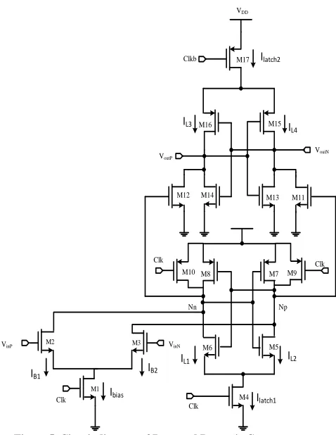
III. PROPOSED COMPARATOR
Although low-voltage low-power double-tail comparator has advantage of having increased ⁄ in order to
enhance latch regeneration speed from positive feedback in gain stage. Yet it suffers from large voltage headroom as it has stacking of four transistors in gain stage. The main idea of proposed comparator is to reduce the stacking transistors along with large ⁄ . To achieve this the drain of the
differential pair transistor is directly connected to the drain of the CMOS cross-coupled inverter to provide strong positive feedback in gain stage as shown in Figure 5. The operation of the proposed dynamic comparator (Figure 5) is as follow. When clock is reset (Clk=0, Clkb = VDD, M1, M4 and M17 are off avoiding static power), PMOS transistors M9 and M10 pulls both node voltages Np and Nn to VDD. The intermediate stage transistors M11 and M12 are on, which make both output node voltages VoutP and VoutN to 0 V. When clock is set (Clk = VDD, Clkb = 0, M1, M4 and M17 are on) transistors M9 and M10 are off. Moreover, at the beginning of the evaluation phase, PMOS transistors M7 and M8 are still off since Np and Nn node voltages are about VDD. Thus Np and Nn starts dropping at different rates according to the applied input voltage (VinP and VinN). Suppose VinP > VinN, Nn node voltage drops faster than that of Np node voltage since M2 provides more current through it than M3. The continuous falling of Nn node voltage starts turning on PMOS transistor M7 pulling the Np node voltage back to VDD forcing another PMOS transistor M8 to remain off causing Nn to discharge completely to 0V. Therefore by the time passing, ∆Np/Nn increases in exponential manner reducing the latch regeneration time.
M4 M5 M6
M8 M7
M14 M13
M16 M15
M12 M11
M17 VDD
Clk Clk
VinP VinN
Np Nn
Clkb
VoutP
VoutN
M1
M2 M3
M9 M10
Clk
Clk
Ibias I
latch1
Ilatch2
IL3 I
L4
IL1 IL2
IB2
[image:5.612.329.568.133.442.2]IB1
Figure 5. Circuit diagram of Proposed Dynamic Comparator.
A. Delay Calculation:
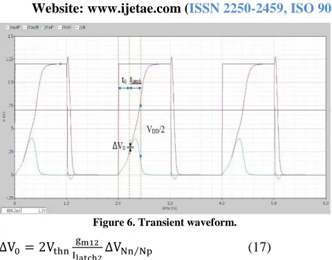
Similar to the low-voltage low-power double tail comparator the delay of proposed comparator is t0 and tlatch as shown in Figure 6 and it also has similar analysis. Hence t0 can be given as
. (16)
International Journal of Emerging Technology and Advanced Engineering
Website: www.ijetae.com (ISSN 2250-2459,ISO 9001:2008 Certified Journal, Volume 4, Issue 8, August 2014)
[image:6.612.49.289.119.307.2]559
Figure 6. Transient waveform.
⁄ (17)
Where gm12 is transconductance of intermediate transistor M12 which is equal to transconductance of M11 (gm11). Also cross-coupled inverter pair M6-M8 and M5-M7 provide positive feedback at Nn/Np node hence ∆VNn/Np can be calculated by using small signal model given in [17] as
⁄ ( ) (( ) ⁄ ) (18)
In this equation,
. At gain stage
M2/M3 are always on increasing the transconductance of input latch inverter pair which is .Where CL,N is the load capacitance of latch of gain stage at node Nn/p,
is the transconductance of gain stage and
( ) is initial node voltage of Nn/Np. Hence
( ) can be calculated from
( ) | |
(19)
Where gm2 = gm3 is the transconductance of M2 and M3. On putting equation (18) in (17), ∆V0 can be obtained as
⁄
| |
(( ) )
(20)
In this comparator during evaluation phase, one of the Nn/Np node get charged back to VDD which turn on one of the transistor M11/M12 thus effective transconductance of latch stage increases ( ) resulting stronger
positive feedback to latch stage.
(
)
(
⁄
) (21)
Form equations (16), (20) and (21) total time delay can be given by
(
⁄ )
( ⁄
| | (( ) ( ) )
)
(22)
From equation (22) it is confirmed that increase in transconductance of input latch inverter ( )
increases ∆V0 in exponential manner reducing overall latch time delay effectively. By comparing the delay expression of all three discussed comparator, the proposed comparator has smaller delay than double-tail latch-type voltage sense amplifier and low-voltage low-power double tail comparator as it enhances the transconductance gain at both gain and latch stage. With lower of stacking transistor it can also be operated at lower supply voltage with high speed.
B. Transient response:
International Journal of Emerging Technology and Advanced Engineering
Website: www.ijetae.com (ISSN 2250-2459,ISO 9001:2008 Certified Journal, Volume 4, Issue 8, August 2014)
[image:7.612.49.293.116.257.2]560
[image:7.612.322.565.121.279.2]Figure 7. Delay of proposed dynamic comparator for ∆Vin = 1 mV, Vcm = 0.7 V and VDD = 1.2 V.
Figure 8. Power of proposed dynamic comparator for ∆Vin = 1 mV, Vcm = 0.7 V and VDD = 1.2 V.
Figure 9. Clock sampling frequency of 2 GHz.
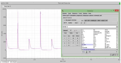
IV. SIMULATION RESULTS
A. Delay comparison:
[image:7.612.49.291.287.414.2]Delay comparison of proposed comparator with some previous comparators are computed by simulating all comparators in cadence virtuoso 180 nm process technology. The simulation are carried out at common mode
Figure 10. Delay comparison of comparators for Vcm = 0.7 and ∆ Vin = 50 mV at sampling frequency 500 MHz.
Figure 11. Power comparison of comparators for Vcm = 0.7 and ∆ Vin = 50 mV at sampling frequency 500 MHz.
voltage Vcm =0.7 V, differential input voltage ∆Vin = 50mv and by varying supply voltage VDD from 0.9 V to 1.4 V at clock sampling frequency of 500 MHz. after simulation the delay is plotted versus supply voltage as shown in the Figure 10. From delay plot it is clear that on lowering the supply voltage delay of each comparator increases along with increase in difference of delay between them.
B. Power comparison:
Power comparison of proposed with some previous comparators are computed by simulating all comparators in cadence virtuoso 180 nm process technology. The simulation are carried out at common mode voltage Vcm = 0.7 V, differential input voltage ∆Vin = 50mv and by varying supply voltage VDD from 0.9 V to 1.4 V at sampling clock frequency of 500 MHz.
200 250 300 350 400 450
0.9 1 1.1 1.2 1.3 1.4
De
lay
(p
s)
Supply Voltage, VDD (V)
Double Tail Latch Type Voltage SA
L-V L-P Double Tail Comparator
Proposed Comparator
0 20 40 60 80
0.9 1 1.1 1.2 1.3 1.4
P
o
w
er
(
µ
W
)
Supply Voltage, VDD (V)
Double Tail Latch Type Voltage SA
L-V L-P Double Tail Comparator
[image:7.612.323.564.307.458.2] [image:7.612.49.291.446.566.2]International Journal of Emerging Technology and Advanced Engineering
Website: www.ijetae.com (ISSN 2250-2459,ISO 9001:2008 Certified Journal, Volume 4, Issue 8, August 2014)
561
After simulation the power is plotted versus supply voltage as shown in Figure 11. From power plot it is clear that on lowering the supply voltage power of each comparator decreases along with decrease in difference of power between them.
C. Comparison between proposed comparator and previous comparators:
The proposed comparator is designed in 180 nm process technology using Cadence Virtuoso tool and compared with the simulation results of previous comparators. The simulation are carried out at common mode voltage Vcm = 0.7 V, differential input voltage ∆Vin = 1 mV for supply voltage of 1.2 V at clock sampling frequency of 500 MHz. The size of each transistor of the comparators are selected in such a way to have optimum output. After simulation, the circuit results show that comparator has 323.0 ps delay time, 38.99 µW power and 3.513 V/ns slew rate for common mode voltage (Vcm) = 0.7, input differential voltage (∆Vin) = 1 mV. The simulation result shows that the proposed comparator has 17.87% smaller delay than double-tail latch-type voltage SA and 16.73% smaller delay than low-voltage low-power double-tail comparator. It also has, 36.6% lower power consumption than double-tail latch-type voltage SA and 31.24% lower power consumption than low-voltage low-power double-tail comparator. From simulation result, it is clear that the proposed comparator has smaller delay, lower power consumption, and has higher speed of operation.
V. CONCLUSION
[image:8.612.316.572.149.587.2]In this paper, two dynamic comparators are analyzed. A new dynamic comparator with pre-amplifier followed by latch stage is presented with low voltage and low power capability using 180 nm process technology, 1.2 V supply voltage and bottleneck operating temperature of 27oC. After simulation, circuit result shows that the proposed comparator has smaller delay, lower power consumption and has higher speed of operation.
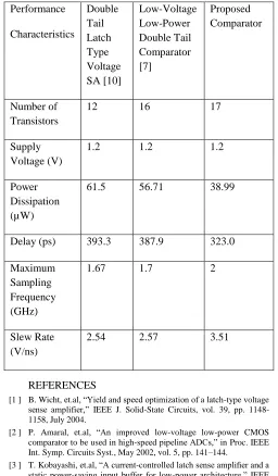
Table 1 Comparison table
Performance
Characteristics
Double Tail Latch Type Voltage SA [10]
Low-Voltage Low-Power Double Tail Comparator [7]
Proposed Comparator
Number of Transistors
12 16 17
Supply Voltage (V)
1.2 1.2 1.2
Power Dissipation (µW)
61.5 56.71 38.99
Delay (ps) 393.3 387.9 323.0
Maximum Sampling Frequency (GHz)
1.67 1.7 2
Slew Rate (V/ns)
2.54 2.57 3.51
REFERENCES
[1 ] B. Wicht, et.al, ―Yield and speed optimization of a latch-type voltage sense amplifier,‖ IEEE J. Solid-State Circuits, vol. 39, pp. 1148-1158, July 2004.
[2 ] P. Amaral, et.al, ―An improved low-voltage low-power CMOS comparator to be used in high-speed pipeline ADCs,‖ in Proc. IEEE Int. Symp. Circuits Syst., May 2002, vol. 5, pp. 141–144.
International Journal of Emerging Technology and Advanced Engineering
Website: www.ijetae.com (ISSN 2250-2459,ISO 9001:2008 Certified Journal, Volume 4, Issue 8, August 2014)
562
[4 ] Jun He, et.al, ―Analyses of Static and Dynamic Random Offset Voltages in Dynamic Comparators,‖ IEEE Trans. Circuits Syst. I: Reg. Papers, vol. 56, pp. 911-919, May 2009.
[5 ] Nikoozadeh and B. Murmann, ―An Analysis of Latch Comparator Offset Due to Load Capacitor Mismatch,‖ IEEE Trans. Circuits Syst. II: Exp. Briefs, vol. 53, no. 12, pp. 1398-1402, Dec. 2006.
[6 ] Pedro M.Figueiredo and Joao C.Vital, ―Kickback Noise Reduction Techniques for CMOS Latched Comparator‖, IEEE Trans. on Circuits and Systems, vol. 53, no.7, pp.541-545, July 2006. [7 ] Samaneh Babayan-Mashhadi and Reza Lotfi, ―Analysis and Design
of a Low-Voltage Low-Power Double-Tail Comparator‖, IEEE Trans. Very Large Scale Integration (VLSI) Systems, vol. 22, no. 2, PP.343-352, February 2014.
[8 ] P. Nuzzo, et.al, ―Noise analysis of regenerative comparators for reconfigurable ADC architectures,‖ IEEE Trans. Circuits Syst. I, Reg. Papers, vol. 55, no. 6, pp. 1441–1454, Jul. 2008
[9 ] K. Uyttenhove and M. Steyaert, ―A 1.8 V 6-bit 1.3-GHz flash ADC in 0.25 µm CMOS,‖ IEEE J. Solid-State Circuits, vol. 38, no. 7, pp.1115–1122, Jul. 2003.
[10 ] D. Schinkel, et.al, ―A Double-Tail Latch-Type Voltage Sense Amplifier with 18ps Setup+Hold Time,‖ ISSCC Dig. Tech. Papers, pp. 314-315 and 605, Feb. 2007.
[11 ] B. Razavi and B. A. Wooley, ―Design techniques for high-speed high-resolution comparators,‖ IEEE J. Solid-State Circuits, vol. 27, no. 6, pp. 1916–1926, Dec. 1992.
[12 ] H.J. Jeon and Y.B. Kim, ―A Low-offset High-speed Double-tail Dual-rail Dynamic Latched Comparator,‖ ACM GLSVLSI’10(Great Lakes Symposium on VLSI), May 16-18, 2010.
[13 ] Philip E. Allen and Douglas R. Holberg, CMOS Analog Circuit Design, 2nd ed. New York, NY: Oxford, 2002.
[14 ] B. Razavi, Principles of Data Conversion System Design. Piscataway, NJ: IEEE Press, 1995.
[15 ] B. Goll and H. Zimmermann, ―A comparator with reduced delay time in 65-nm CMOS for supply voltages down to 0.65,‖ IEEE Trans. Circuits Syst. II, Exp. Briefs, vol. 56, no. 11, pp. 810–814, Nov. 2009.
[16 ] Marcel J.M. Pelgrom, Analog-to-Digital Conversion, Springer Science+Business Media B.V. 2010.
![Figure.1 shows schematic of double-tail latch-type voltage sense amplifier [10]. For its operation, during](https://thumb-us.123doks.com/thumbv2/123dok_us/8710706.881836/2.612.77.261.135.441/figure-shows-schematic-double-latch-voltage-amplifier-operation.webp)
![Figure 3 shows a low-voltage low-power double-tail comparator [7]. It is basically a modified form of double-](https://thumb-us.123doks.com/thumbv2/123dok_us/8710706.881836/3.612.339.547.127.435/figure-shows-voltage-double-comparator-basically-modified-double.webp)