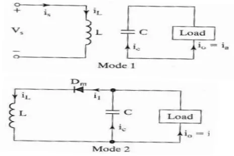
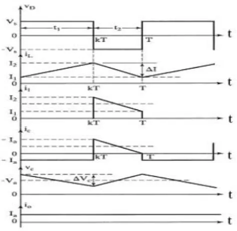
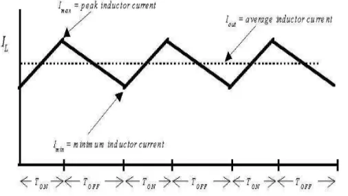
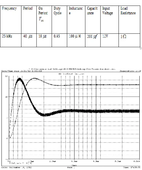
Design and Simulation of DC DC Converters
Full text
Figure


Related documents
4.1 The Select Committee is asked to consider the proposed development of the Customer Service Function, the recommended service delivery option and the investment required8. It
National Conference on Technical Vocational Education, Training and Skills Development: A Roadmap for Empowerment (Dec. 2008): Ministry of Human Resource Development, Department
Currently, National Instruments leads the 5G Test & Measurement market, being “responsible for making the hardware and software for testing and measuring … 5G, … carrier
• Follow up with your employer each reporting period to ensure your hours are reported on a regular basis?. • Discuss your progress with
Marie Laure Suites (Self Catering) Self Catering 14 Mr. Richard Naya Mahe Belombre 2516591 [email protected] 61 Metcalfe Villas Self Catering 6 Ms Loulou Metcalfe
The corona radiata consists of one or more layers of follicular cells that surround the zona pellucida, the polar body, and the secondary oocyte.. The corona radiata is dispersed
expanding host range of DMV, testified by the present report and by numerous cases of DMV infection reported in the last 5 years in the Mediterranean Sea ( Mazzariol et al., 2013,
Home health care 30% co-ins Not Covered Coverage is limited to 60 visits per calendar year. Not covered without
