http://dx.doi.org/10.4236/ica.2015.62012
How to cite this paper: Smoliński, Ł., Barkalov, A. and Titarenko, L. (2015) Adaptation of the Two Sources of Code and One-Hot Encoding Method for Designing a Model of Microprogram Control Unit with Output Identification. Intelligent Con-trol and Automation, 6, 116-125. http://dx.doi.org/10.4236/ica.2015.62012
Adaptation of the Two Sources of Code
and One-Hot Encoding Method for Designing
a Model of Microprogram Control Unit with
Output Identification
Łukasz Smoliński
*, Alexander Barkalov, Larysa Titarenko
Institute of Computer Engineering and Electronics, University of ZielonaGóra, Zielona Góra, Poland Email: *[email protected]
Received 4 March 2015; accepted 9 April 2015; published 10 April 2015
Copyright © 2015 by authors and Scientific Research Publishing Inc.
This work is licensed under the Creative Commons Attribution International License (CC BY).
http://creativecommons.org/licenses/by/4.0/
Abstract
This article presents a proposal for a model of a microprogram control unit (CMCU) with output identification adapted for implementation in complex programmable logic devices (CPLD) equipped with integrated memory modules [1]. An approach which applies two sources of code and one-hot encoding has been used in a base CMCU model with output identification [2] [3]. The article de-picts a complete example of processing for the proposed CMCU model. Furthermore, it also
dis-cusses the advantages and disadvantages of the approach in question and presents the results of the experiments conducted on a real CPLD system.
Keywords
CPLD, PAL, UFM, CLB, Two Sources of Code, One-Hot Encoding, CMCU
1. Introduction
Nowadays, complex programmable electronic systems are applied for implementing logic circuits of control units [4]-[9]. However, the issue of reducing the size of a control unit is still a subject of current interest [10] [11]. Reducing the size of used resources makes it possible to improve such indicators as: the speed of perfor-mance, power consumption and the size of the realised unit [12] [13]. One of the methods for reducing the size of the control unit is the realization of the control algorithm with the use of the CMCU (compositional micro-program control unit) project methodology [14]. The application of CMCU makes it possible to implement a
much smaller number of logical functions realising the task of the control system. The existing project methods based on the CMCU are not dedicated to the solutions realized with the use of programmable devices (CPLD). CPLDs include macrocells of programmable array logic (PAL) with a limited number of terms. To reduce the amount of hardware in the logic circuit of a control unit, the peculiarities of the CPLD and the features of a con-trol algorithm to be implemented should be taken into account. Some of the CPLD family devices are equipped with integrated memory. For example, Altera CPLD devices are equipped with user flesh memory (UFM) [15], whereas Cypress CPLD devices are equipped with cluster memory blocks (CMB) [16]. This article presents a mathematical model and a design algorithm with two sources of code and one hot encoding which has been adopted to CMCU model with output identification [1].
2. Background of the CMCU with Output Identification
It is assumed that the graph-scheme of the algorithm (GSA) is represented by sets of vertices B where
{
}
1 2 0, E
B=B B b b and a set of arcs E where E=
{
b bt, q}
. It is further assumed that b bt, q∈B and b0is an initial vertex, bE is a final vertex, B1 is a set of operator vertices, B2 is a set of conditional vertices. A
vertex contains a microinstruction mi∈M i
(
=1,,B1)
and mi is a set of data-path microoperations{
1, , N}
Y = y y [17]. Each vertex bt∈B2 contains a single element xi of a set of logical conditions
{
1, , L}
X = x x . A set C of operational linear chains (OLC) for the GSA shall be formed, where each OLC is a sequence of operator vertices and each pair of its adjacent components corresponds to an arc of the GSA.
{
1, , i}
.C=
α
α
(1)Each OLC αi has only one output Oi and an arbitrary number of inputs Iij. The αi elements are unders-tood as a state of the system which is identified by Oi elements. OLC outputs make up the collection Oi∈ ΠC. Each vertex from bt∈B1 corresponds to microinstruction mi∈M stored in the control memory (CM) of CMCU and it has an address A b
( )
t . The microinstructions can be addressed using R bits, where2 1
log ,
R= M M = B (2)
and the bits are represented by variables from the set T:
{
1, , R}
.T = T T (3)
The project methodology of the microprogram control unit with output identification offers specific position-ing of microinstructions in the memory, so as to make it possible to determine the state of the unit, usposition-ing possi-bly the smallest number of address signals. The algorithm of positioning microinstruction in the memory con-sists of the following steps:
1. First, all microinstruction addresses are coded with the use of natural encoding.
2. The value of ROI is set to ROI = log2 C.
3. An address table is created. The table consists of 2ROI columns defined as
OI
R of older address bits, and
5
2R−ROI lines defined as
5 OI
R −R younger address bits, where R5=R, following Equation (2).
4. If the outputs Oi i Oj of two different OLC chains
α α
i, j∈C, where j>i belong to the same column and neither of the outputs is connected with the end vertex of the network of operations Γ, then the data are moved to the right, beginning with the first vertex of the chain αi. The released cells are determined as “in-significant” with the symbol * . The operation of moving to the right is repeated until the outputs Oi andj
O are placed in separate columns of the table.
5. If all the output vertices are uniformly represented by ROI, then the algorithm moves to step 7.
6. If the address of any vertices reaches beyond the range of the current addressing, then: ROI =ROI+1. Next, the algorithm returns to step 4.
7. The end.
The codes for each microinstruction are formed as a concatenation of the table’s columns and lines. In such a case, the outputs of the OLC chain are uniformly encoded using variables from the set T′ where:
.
, OI
The algorithm for designing a model of the CMCU with output identification consists of the following steps: 1. Formation of the set of OLCs.
2. Addressing microinstructions (with shifting operation) and encoding OLC elements. 3. Formation of the control memory content.
[image:3.595.170.428.608.704.2]4. Formation of the transition table of the CMCU. 5. Formation of the excitation function for the counter. 6. Synthesis of the logic circuit of CMCU.
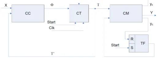
Figure 1 shows a logical scheme of the CMCU with output identification. The pulse Start causes loading
of the first microinstruction address into a counter CT and set up of a fetch flip-flop TF. If Fetch=1, then mi-croinstructions can be read out of the control memory CM. If a current microinstruction does not correspond to an OLC output, then a special variable y0 is formed together with microoperations Yq⊆Y. If y0 =0, then content of the CT is incremented according to the addressing mode. Otherwise, the block of CC generates func-tions Φ. If yE equals 1, then the CMCU stops and new data from the CM will be not loaded.
3. Main Idea behind
the Proposed Method
It shall be pointed out that the logic for the CC and CT is implemented as parts of the CPLD. An external PROM chip or memory integrated with the CPLD may be applied to implement the CM. The memory has t outputs, where t=2, 4,8,16, 32 [18]. Some information can be implemented using free outputs of the CM. It is as-sumed that one-hot encoding of microoperations is used. The word of the CM has
0 2.
R = +N (5)
The R2 outputs of the CM are free:
2 0.
R = −t R (6)
The R2 bits are represented by variables from the collection P:
{
1, , R2}
.P= p p (7)
If conditions
2 0, 2 OI
R > R <R (8)
take place, the method can be used. As for encoding additional information used by excitation functions for the CT, one-hot encoding will be applied. In such a case, the amount of information that can be stored in free CM is:
2. one hot
I − =R (9)
Next, an occurrence table is created, with columns Oi and gi. The Oi column contains the OLC elements, whereas the gi column shows the number of occurrences of an OLC element while making an excitation func-tion for the CT. The number of occurrences of the Oi element is counted on the basis of a transition table, where a number of high bits is counted in addresses corresponding to Oi. Using the occurrence table, it is now possible to transfer the Ione hot− of the most frequently used Oi elements to a new collection:
.
i B
O∈ Π (10)
.
C A B
Π =Π Π (11) For the CMCU model with output identification and two sources of code, the memory CM is a source of va-riables pi∈P used for encoding the elements Oi∈ ΠB through codes KB
( )
Oi . The ROI of the oldest output bits from the counter CT is a source of variables from the set T′ used for encoding the elementsA i
O ∈ Π through codes KA
( )
Oi .It shall be highlighted that the maximum length of the logical expressions used for making excitation func-tions which use the information from the source ΠC for the base method of the CMCU with output identifica-tion is:
.
C OI
L = X +R (12)
For the proposed model with one hot encoding, the maximum length of the logical expressions built on the basis of the information from the collection ΠA does not change and equals:
.
A OI
L = X +R (13)
The maximum length of logical expressions for the model with one hot encoding, built on the basis of the in-formation from the collection ΠB, is reduced and equals:
1. B
L = X + (14)
As a result, the value of the CM and the transition table have been modified on the basis of the occurrence ta-ble.
The modified algorithm for designing a model of the CMCU with output identification consists of the follow-ing steps:
1. Formation of the set of OLCs.
2. Addressing microinstructions (with shifting operation) and encoding OLC elements. 3. Formation of the control memory content.
4. Formation of the transition table of the CMCU. 5. Formation of the occurrence table.
6. Modification of the control memory content. 7. Modification of the transition table of the CMCU.
8. Formation of the excitation function for the counter and minimization. 9. Synthesis of the logic circuit of CMCU.
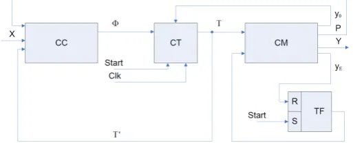
Figure 2 presents a modified structure of the CMCU with output identification and the applied method of two sources of code.
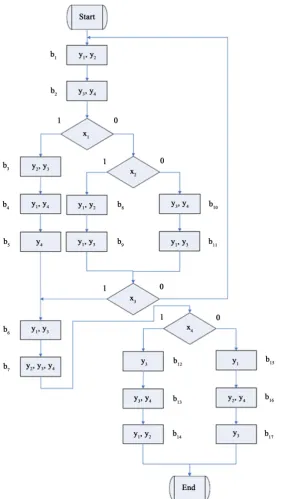
[image:4.595.171.428.591.695.2]4. An Example of the Proposed Method
Figure 3 and Figure 4 present an exemplary algorithm used for the realization by the control unit. This algo-rithm employs the following variables: B1=
{
b1,,b17}
, B2={
x x x x1, 2, 3, 4}
, C={
α1,,α6}
, M =17,5
R= , α =1 b b1, 2 , α =2 b3,,b7 , α =3 b b8, 9 , α =4 b10,b11 , α =5 b12,b13,b14 , α =6 b15,b16,b17 ,
{
6, 5, 4, 3, 2, 1}
C O O O O O O
Π = , ROI =3, Y =
{
y1,,y4}
, N=4. First, an initialization Table 1 of microin-struction addresses is formed.Figure 3. An example of the algorithm used for the realisation of T1.
Table 1. Initial table of addressing.
, , 5 4 3 , 2 1
T T T
T T 000 001 010 011 100
00 1
1 1
b =I b5 b9=O3 b13 b17=O6
01 b2=O1
2
6 2
b =I 1
10 4
b =I b14=O5 *
10 1
3 2
b =I b7=O2 b11=O4
1 15 6
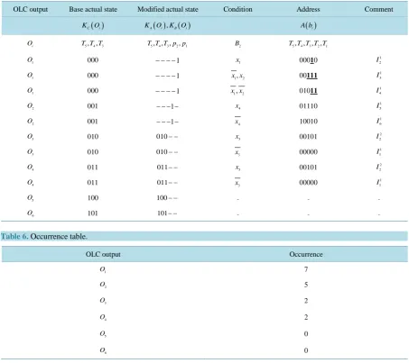
[image:5.595.90.537.627.721.2]Figure 4.Operation chains for the algorithm T1.
Next, the shift operation takes place, resulting in a new address Table 2. Thanks to the shift operation, all the elements Og∈ ΠC may be identified using ROI of older address bits: T′ =
{
T T T5, 4, 3}
. With the use of Table 2, Table 3 is created, containing encoding for operation chains, as well as Table 4, with the content of the CM. Finally, a transition Table 5 is created.Let us assume that we have a memory module in which t=8. Following the above-presented modification, the calculations may be put forward as: R0 =N+ =2 6, R2 = −t R0 =2, Ione hot− =R2=2, where R2 is the
number of free CM bits which will be represented by a set of variables P=
{
p p1, 2}
. On the basis of Table 5,an occurrence Table 6 is created. For the purpose of this example, high values in address bits (there are 7 of them) corresponding to the element O1 have been bolded and underlined in Table 5. The collection ΠC is di- vided into collections ΠB and ΠA. As a result: Π =B
{
O O1, 2}
and Π =A{
O O O O3, 4, 5, 6}
. Next, elementsfrom the collection ΠB are encoded with the use of variables from the set P. As a result: KB
( )
01 = p1,( )
02 2B
K = p . Column 3 in Table 5 contains modified encoding for the OLC elements with a second source of information about the state of the unit, which is a CM module. Table 4 is modified with additional data inform-ing about the state of the unit. These data have been marked with an underlininform-ing and boldinform-ing in columns p1 and p2. The last step is the construction of an excitation function based on the modified data from columns 3 and 4 of Table 5:
Table 2. Table of addressing after shift operation.
, , 5 4 3 , 2 1
T T T
T T 000 001 010 011 100 101
00 1
1 1
b =I b5 b9=O3 b11=O4 b14=O5 b17=O6
01 b2=O1
2
6 2
b =I * * * *
10 1
3 2
b =I b7=O2 *
1 12 5
b =I 1
15 6
b =I *
11 b4
1
8 3
b =I 1
10 4
b =I b13 b16 *
Table 3.OLC elements encoding.
OLC outputs KC(Oi)
Oi T5 T4 T3
O1 0 0 0
O2 0 0 1
O3 0 1 0
O4 0 1 1
O5 1 0 0
[image:7.595.90.536.358.722.2]O6 1 0 1
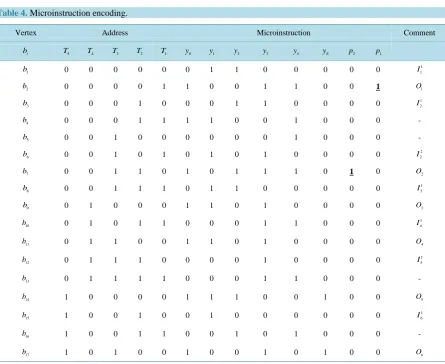
Table 4. Microinstruction encoding.
Vertex Address Microinstruction Comment
t
b T5 T4 T3 T2 T1 y0 y1 y2 y3 y4 yE p2 p1
1
b 0 0 0 0 0 0 1 1 0 0 0 0 0 1
1
I
2
b 0 0 0 0 1 1 0 0 1 1 0 0 1 O1
3
b 0 0 0 1 0 0 0 1 1 0 0 0 0 1
2
I
4
b 0 0 0 1 1 1 1 0 0 1 0 0 0 -
5
b 0 0 1 0 0 0 0 0 0 1 0 0 0 -
6
b 0 0 1 0 1 0 1 0 1 0 0 0 0 2
2
I
7
b 0 0 1 1 0 1 0 1 1 1 0 1 0 O2
8
b 0 0 1 1 1 0 1 1 0 0 0 0 0 1
3
I
9
b 0 1 0 0 0 1 1 0 1 0 0 0 0 O3
10
b 0 1 0 1 1 0 0 0 1 1 0 0 0 1
4
I
11
b 0 1 1 0 0 1 1 0 1 0 0 0 0 O4
12
b 0 1 1 1 0 0 0 0 1 0 0 0 0 1
5
I
13
b 0 1 1 1 1 0 0 0 1 1 0 0 0 -
14
b 1 0 0 0 0 1 1 1 0 0 1 0 0 O5
15
b 1 0 0 1 0 0 1 0 0 0 0 0 0 1
6
I
16
Table 5.Transition table.
OLC output Base actual state Modified actual state Condition Address Comment
( )
C i
K O KA( )Oi ,KB( )Oi A b( )t
i
O T T T5, 4, 3 T T T p p5, 4, ,3 2, 1 B2 T T T T T5, 4, 3, 2, 1
1
O 000 − − − −1 x1 00010
1 2
I
1
O 000 − − − −1 x x1, 2 00111
1 3
I
1
O 000 − − − −1 x x1, 2 01011
1 4
I
2
O 001 − − − −1 x4 01110
1 5
I
2
O 001 − − − −1 x4 10010
1 6
I
3
O 010 010− − x3 00101
2 2
I
3
O 010 010− − x3 00000
1 1
I
4
O 011 011− − x3 00101
2 2
I
4
O 011 011− − x3 00000
1 1
I
5
O 100 100− − - -
-6
O 101 101− − - -
-Table 6. Occurrence table.
OLC output Occurrence
1 O 7 2 O 5 3 O 2 4 O 2 5 O 0 6 O 0
4 1* 1* 2 2* 4, T = p x x +p x
3 1* 1* 2 2* 4 5* 4* 3* 3 5* 4* 3* 3 1* 1* 2 2* 4 5* 4* 3, T = p x x +p x +T T T x +T T T x = p x x +p x +T T x
2 1* 1 1* 1* 2 1* 1* 2 2* 4 2* 4 1 2, T = p x +p x x +p x x +p x +p x = p +p
1 1* 1* 2 1* 1* 2 5* 4* 3* 3 5* 4* 3* 3 1* 1 5* 4* 3. T =p x x +p x x +T T T x +T T T x =p x +T T x
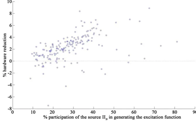
5. Results and Conclusions
Figure 5 presents the results of the implementation of the model in real hardware. The Alter, a family MAX II device EPM1270 F256C5 equipped with UFM, has been used for tests. Figure 5 depicts the relationship be-tween the obtained reduction in the size of the system (in percentage) and the participation of the source of data
B
[image:8.595.86.540.100.503.2]Figure 5.Reduction in the size of the system due to the participation of the source.
1. Formation of the set of OLCs.
2. Addressing microinstructions (with shifting operation) and encoding OLC elements. 3. Formation of the control memory content.
4. Formation of the transition table of the CMCU.
5. Construction of excitation functions for the CT and RG. 6. Minimization of excitation functions.
7. Finding logical expressions—OLC elements which have not undergone minimization—in the minimized ex-citation functions.
8. Formation of the occurrence table containing most frequently occurring OLC elements which have not un-dergone minimization.
9. Modification of the control memory content.
10.Modification of the transition table and CM of the CMCU.
11.Formation of the excitation function for the counter and minimization. 12.Synthesis of the logic circuit of CMCU.
Taking the OLC elements, which do not undergo minimization to the collection ΠB will make it possible to avoid the effect of degradation of minimization possibilities in excitation functions. This effect appears in the scenarios with minor participation of the ΠB source in the construction of the excitation functions. The solu-tion presented in this paper requires formalizasolu-tion of mathematical descripsolu-tions and adaptasolu-tion to specific CMCU models. This proposal also requires conducting implementation experiments based on real reprogramm-able devices. Future studies will focus on designing mathematical models based on the above-presented algo-rithm and comparing the results obtained with the results for the models using the method of two sources of code [2] [3] [19]-[21].
Information
References
[1] Wiśniewski, R. (2009) Synthesis of Compositional Microprogram Control Units for Programmable Devices. Universi-ty of Zielona Gora Press, Poland.
[2] Barkalov, A., Titarenko, L. and Smoliński, L. (2014) CMCU Model with Base Structure Dedicated for CPLD Systems.
Przegląd Elektroniczny, 12, 25-29.
[3] Barkalov, A., Titarenko, L. and Smoliński, L. (2012) Optimization of Control Unit Based on Construction of CPLD,
Pomiary, Automatyka, Kontrola, 58, 93-96.
[4] Monmasson, E., Idkhajine, L., Cirstea, M., Bahri, I., Tisan, A. and Naouar, M. (2011) FPGAs in Industrial Control Applications. IEEE Transactions on Industrial Informatics, 7, 224-242. http://dx.doi.org/10.1109/TII.2011.2123908
[5] Kania, D. (2004) The Logic Synthesis for the PAL-Based Complex Programmable Logic Devices. Zeszyty Naukowe,
Elektronika, 14, 5-212.
[6] Kubica D. and Kania D. (2011) Synteza logiczna zespołu funkcji ukierunkowana na minimalizację liczby wykorzys-tywanych bloków logicznych PAL w oparciu o zmodyfikowany graf wyjść. Pomiary, Automatyka, Kontrola, 57, 737- 740.
[7] Monmasson, E. and Cirstea, M. (2007) FPGA Design Methodology for Industrial Control Systems—A Review. IEEE Transactions on Industrial Informatics, 54, 1824-1842. http://dx.doi.org/10.1109/TIE.2007.898281
[8] Garcia-Vargas, I., Senhadji-Navarro, R., Jimenez-Moreno, G., Civit-Balcells, A. and Guerra-Gutierrez, P. (2007) ROM- Based Finite State Machine Implementation in Low Cost FPGAs. IEEE International Symposium on Industrial Elec-tronics, Vigo, 4-7 June 2007, 2342-2347. http://dx.doi.org/10.1109/ISIE.2007.4374972
[9] Rafla, N. and Davis, B. (2006) A Study of Finite State Machine Coding Styles for Implementation in FPGA. 49th IEEE International Midwest Symposium on Circuits and Systems, Puerto Rico, 6-9 August 2006, 337-341.
[10] Czerwiński, R. and Kania, D. (2009) Synthesis of Finite State Machines for CPLDs. International Journal of Applied Mathematics and Computer Science, 19, 647-659. http://dx.doi.org/10.2478/v10006-009-0052-0
[11] Anand, B.P. and Saravanan, C.G. (2012) Development of Research Engine Control Unit Using FPGA-Based Embed-ded Control System. Journal of KONES Powertrain and Transport, 19, 9-18.
[12] Salauyou, V. and Grzes, T. (2007) FSM State Assignment Methods for Low-Power Design. 6th International Confe-rence on Computer Information Systems and Industrial Management Applications, 2007, CISIM ’07, Minneapolis, 28- 30 June 2007, 345-350.
[13] Czerwinski, R. and Kania, D. (2012) Area and Speed Oriented Synthesis of FSMs for PAL-Based CPLDs. Micropro-cessors and Microsystems, 36, 45-61. http://dx.doi.org/10.1016/j.micpro.2011.06.004
[14] Barkalov, A. and Titarenko, L. (2008) Logic Synthesis for Compositional Microprogram Control Units. Springer, Ber-lin.
[15] Altera (2007) Using the UFM in MAX II Devices. www.altera.com/literature/an/an489.pdf
[16] Cypress (2003) Delta39K ISR CPLD Family.
http://pdf.datasheetcatalog.com/datasheet2/9/0pfaeyx4ushkk0zzjksaycgxhqky.pdf
[17] Baranov, S. (2008) Logic and System Design of Digital Systems. TUT Press, Tallin.
[18] Maxfield, C. (2004) The Design Warrior’s Guide to FPGAs: Devices, Tools and Flows. Elsevier, Amsterdam.
[19] Barkalov, A., Titarenko, L. and Smoliński, L. (2013) Hardware Reduction for Compositional Microprogram Control Unit Dedicated for CPLD Systems. Proceedings of IEEE East-West Design and Test Symposium-EWDTS 2013, Ros-tov-on-Don, 27-30 September 2013, 1-6. http://dx.doi.org/10.1109/EWDTS.2013.6673200
[20] Barkalov, A., Titarenko, L. and Smoliński, L. (2014) The Application and Adaptation of the Two Sources of Code and Natural Encoding Method for Designing a Model of Microprogram Control unit with Base Structure. Circuits and Sys-tems, 5, 301-308. http://dx.doi.org/10.4236/cs.2014.512031
[21] Barkalov, A., Titarenko, L. and Smoliński, L. (2011) Optimization of Microprogram Control Unit with Code Sharing.
Proceedings of IEEE East-West Design & Test Symposium-EWDTS 2011, Sevastopol, 9-12 September 2011, 55-59.