TABLE OF"CONTENTS
PAGE NO.
001
BATTERY BACKUP
1
005
IEEE Bus SUB-SPECS
4
009
HEX AND QUAD HOLD-DoWN BRACKET FOR LSI-II
5
SYSTEMS
OIOA
POWER SUPPLY FOR H909C
6
011
LSI-II HALTING DURING INTERRUPT CYCLE
8
012
LSI-II Bus THEORY OF OPERATION
10
013
INSTALLING APL-l1 ON 11V03 AND 11T03
19
014
CORRECT INPUT PARAMETERS FOR THE QJV1l PROM
20
FORMATTING PROGRAM
015
POWER SEQUCENCING FOR THE KD1l-HA MODULE
22
017
LSI-11/2 PROCESSOR CLOCK
25
018
DRl1-C vs. DRVII
26
019
EIA RS-422 AND RS-423
30
020
9 X
6 SLOT BACKPLANE DOCUMENTATION ERROR
34
021
COMPARISON OF DATA TRANSMISSION TECHNIQUES
35
023
USING THE MSVll-D 30K OPTION
40
024A
ASYNC.~SERIAL LINE UNIT COMPARISONS
41
025
CONFIGURING MEMORY SYSTEMS WITH MSVll-D
46
RAM
&
PROM
026
MICRO BACKPLANE MECHANICAL MOUNTING
48
GUIDELINES
027A
PROM CHIPS AVAILABLE UNDER PART
#
MRVll-AC
56
028
EXTENDED MEMORY FOR THE LSI-II
57
029
USING THE MRVII-AA FOR A BOOTSTRAP ROM
69
030
SRUN SIGNAL
71
032
EXTENDED Bus TIME-OUT LOGIC
73
PAGE
NO.
034
CONFIGURING A 3-Box 11/03 SYSTEM
78
035
PROM PROGRAMMING
80
036
CORE MEMORY IN 11/03-L BACKPLANE
81
037
C-D INTERCONNECT SCHEME
82
038
DIAGNOSTICS FOR 30K MEMORIES ON LSI-II's
85
039
DMA REQUEST/GRANT TIMING
86
040
PATCHES FOR BASIC/PTS ON LSI-II
88
041
NEW FUNCTIONALITY FOR BDVll-AA BOOT
90
042
REMOVING f10DULES FROM "LIVE" BACKPLANES
91
043
BACKPLANES FOR THE RLVl1 (RL01)
93
044
CONSOLE ODT "L" COMMAND ON 30K SYSTEMS
95
046A
DLVII-F REPLACEMENT FOR THE DLVII
96
047
INCOMPATIBILITY BETWEEN THE REVII AND
99
THE LS I -11/23
048
LSI-ll/23 INSTRUCTION TIMING (PRELIMINARY)
101
049
SYSTEM DIFFERENCES - LSI-II VS. LSI-ll/23
111
050
MICRO ODT DIFFERENCES - LSI-II VS. LSI-ll/23
113
051
DIGITAL SUPPORTED PROM's
116
052
PARITY MEMORY IN LSI-ll/23 SYSTEMS
117
053
PDP-II FAMILY DIFFERENCES
125
054
MXVII CONFIGURATION
136
055
LSI-II VS. LSI-ll/23 Bus TIMING
141
056
DLVII-J CABLI NG
143
057
LOCATION OF W13 ON THE BDVII
147
058
CONFIGURING MEMORY FOR LSI-II SYSTEMS
149
WITH MORE THAN 64K BYTES
PAGE NO.
061
PROGRAMMING THE MRV11-C
164
062
BOOTSTRAPS FOR TU58
1RL01
1RK05
1RX02
1RX01
173
063
RLOI TYPE-IN BOOTSTRAP
204
064
DLV11-J
1/0
PAGE ADDRESS PROBLEM REPORT
205
065
BOOTSTRAP FOR RX02
207
066
11/23
FLOATING POINT
CO~IPATIBILITY210
067A
DLV11-J RECEIVER CHIP PROBLEM
211
068
MICROCOMPUTER MODULE ENVIRONMENTAL
213
CONSIDERATIONS
069
18-BIT DMA WITH CHIPKITS
214
070
LSI-II
vs.
LSI-11/23 TRANSACTION DIFFERENCES
216
071
EXPANDING BA11-MA AND BA11-NC BASED SYSTEMS
218
072
PERIPHERAL COMPATIBILITY WITH 11/23 SYSTEMS
221
073
TU58 CABLING
223
074
MXV11-AAI -AC CABLING
225
075
MXV11-A2 BOOTSTRAP ERROR HALTS
227
077
SUMMARY OF BOOTSTRAP SOURCES
230
078
LSI-11/23 PROCESSOR DIFFERENCES
231
079
THE LSI-11/23 AND THE LSI-11/2 BUSES ARE
233
THE SAME
080A
LSI-11/23 1/0 PAGE ADDRESSING
234
081
USE OF RECOMMENDED DISKETTES
236
082
HANDLERS FOR SERIAL LINE PRINTERS
237
083
ALTERNATE CLOCK FREQUENCIES FOR THE MXV11
248
084
IMPROVED DLV11-F
250
-.
).Inote
NUMBER 001DATE
TITLE BATTERY BACKUP 4
/
1 /77DISTRIBUTION UNRESTRICTED PRODUCT
MSV11-C (M79SS) ORIGINATOR JOE AUSTIN
PAGE 1 OF3
SCOPE
The function of this note is to furnish the information necessary to provide battery backup for the MSVII-C 16K MaS RAM module. Specific recommendations for the battery, charger, and DC-DC converters will not be covered at this time.
Additional information on the MSV11-C is contained in the "MSVIl-C Users Manual", document number EIC-NSV11-0P.
SYSTEM DESCRIPTION
A block diagram showing two MSVI1-C aodules providing 28I words of memory is shown in Figure 2. Bach 16K module is plugged into a standard backplane with the battery power connected to pins AVI (+SV) and ASl (+12V) as shown. These two voltages are sourced by DC-DC converters/regulators which are connected directly to the battery. A charger is provided which is
connected to the battery and converters by control logic. The function of the control logic is to disconnect the charger when AC power is lost, to disconnect the battery from the
converters when it discharges too low, and to switch to a trickle-charge once the battery has been fully charged.
FUNCTIONAL REQUIREMENTS
To properly implement this system, the following conditions must be met:
l~ The battery power required to back up the two modules is:
+SV +3' +12V +3'
1.6 A type (2.8A aax) 0.32 A type (O.4A max)
These voltages must remain within +3' of the voltages for the LSI-II at all times, and aust not change by aore than +3\ during the transition~DD~erom the battery.
2.
)Jnote
PAGE 2 OF3 NUMBER 001All MSVll-C modules using battery backup aust be at etch Rev. D. Those modules at etch Rev. C must have ECa No. I for aodule M79SS installed. This ECa adds the circuit shown in Figure 1 in the following manner:
• cut the etch to free pins E31-S and E31-10
• add wires from E18-12 to E20-9 E19-12 to E20-10 E20-14 to E31-S
&
103. The following jumpers should be configured as shown:
4.
S.
6.
7.
WI. WS - Remove to separate the battery power from the bussed system power.
W2. W3 - Insert to connect the battery power to the refresh logic.
W6 • • 7 - Insert to enable internal refresh and to prevent the aodule from asserting BRPLY during refresh.
The heat generated by the refresh logic on each MSVII-C is 8 watts. Alternate cooling .ust be providfed to dissipate this heat if the AC fans are off for aore than tWiO minutes.
Certain precautions should be tajken in the design of the power sequencing logic and other specilll modules. Signal BSYNC m,st be driven by a source tbat has a hiJ~h impedance when power is removed from the rest of the system. Signals BDCOK and BPOK must be driven by a low impedance source (less than 8 ohms) under the same condition and should have no bounce (no relay). A J-FET is recommended since it also provides the necessary rise and fall times. These precau-tions have been taken in those systems using the H780-H or J power supply as provided by PDP-ll/03 ()r PDP-IIV03 systems.
All master (DNA) modules aust fiIlish gracefully when BPOK indicates an AC power failure. Any cycles in process .ust be allowed to
finish. should be off the bus within two microseconds. and must not hang up signal BSYNC.
The software .ust finish its powE~r-down procedure and issue a HALT instruction within two milliseconds from the time signal BPOK
indicates an AC power failure.
(EI8-12) DCOK L
(EI9-12) Lockout H :01
8:::~
Lockout A
L
(E31-S & 10)FIGURE I~Dm_LOGIC
COMPONENTS
eiReMlP
FIGURE 2. TYPICAL BATTERY BACKUP SYSTEM
MSV11-C MSV11-C
16K 12K
BACKPLANE
AV1* AS1*
GND
+5 DC-DC CONVERTER
BATTERY CHARGER
AC INPUT
+5V +12V GND
+12 DC-DC CONVERTER
DC
CONTROL LOGIC
BATTERY
~D~DDmD
COMPONENTS
NUMBER
DATE
TITLE, __ ~I~E~B~E~B~U~S~S~U~B~-S~P~B~C~S ____ . ____________ _ S /2
h7
DISTRIBUTION....-_l~B~V~I~l_C~U~'S~T~O~ME_RS~. ____ ---__ __ PRODUCTORIGINATOR JOB AUSTIN
PAGE OF
The IBVII-A, when connected to the LSI-!l, will meet the following subsets of IBEE Standard
488-1975:
SHI SRl CI
AHI RLI C2
TS PP2 C3
TBS DCI C4
L3 DTl CS
LB3
This module is designed to be th4! only controlle1" on the IEEB bus. Therefore, it will not respond to another controller on the bus that issues either a parallel' poll configure command or a parallel poll control signal (subset PP2)~
~IJ~DDmD
COMPONENTS
CiROUP
),Inote
NUMBER 009DATE
·'ITLE HEX AND ~UAD HOLD-DOWN BRACKET FOR 6 / 6 / 77
LSI-II S
STEMSPRODUCT LSIo.ll HSTRIBUTION UNRESTRICTED
M ~UNTING HARDWARE
DRIGINATOR JOHN HUGHES
PAGEl Oli
Here is a product that will help in applications that require a mechanically rigid system with double-sized modules in a 4x4 back-plane or any time the 9x6 backback-plane is used. The hold-down bar that is described in the following clipping from the 1977-78 Logic Handbook (page 369) describes the same hold-down bracket that is
u.sed on quad-sized modules, like the LSI-II processor and the MSVII-CD
memory board.
To use this bracket, customers can drill out the existing handles on double or quad-sized board and attach the bracket by means of either rivets or screws.
In addition to offering increased rigidity and resistance to vibration, this bracket makes insertion and removal of modules far easier.
Hold-Down Bracket 12-10711'()2
The 12~10711-02 module hold-down bracket serves as a mechanical com-bination handle arid hold-down bracket for Hex-size modules when used with the appropriate cards guides such as an' H0341. . This bracket can also be used as a hold-down bracket for LSI-ll compatible modules (quad-size) but must be modified as shown in the accompanying drawing.
LSI-ll HOLDOWN 12-10711'()2
1_ CUT BRACKET AT POINTS DESIGNATED ON DRAWING BELOW. 2. DISCARD CENTER SECTION "B".
3. MOUNT SECTIONS "A" AND "C" ON BOARD AS DESIRED.
~D~DD~D
COMPONENTS
).Inote
NUMBER 010ADATE
TITLE Power Supply For H909C 6 /7 17
DISTRIBUTION H909C Customers PRODUCT
H909C ORIGINATOR David Schanin
PAG~
of2
THIS MICRO NOTE REPLACES 1010. 1010 SHOULD BE DISCARDED AND REPLACED WITH THIS ONE AS IT WAS IN ERROR.
---~---~~---~----The H909C Expander Box is a convE~nient" way to package the DDVI1-B 9x6 ba~kplane with the H0341 card guide. However, the H780 power supply may not be used with the H909C because air flow from the power supply fans will be restricted. Customers must provide their own power supplies and provide for cooling of both the LSI-II cards and the power supplies.
There are two configurations of I"ambda power supplies that have the potential of powering the H909C module systems enclosure. One is a 148-watt configuration that sells for $400 and the other is a 321-watt configuration that sells for $760.
The 321-watt configuration requires two +12 volt supplies to be connected in parallel. This is accomplished by connecting a
diode in series with each positi,re output and connecting the sense input on the load side of the diode. One supply will current
limit and the other will regulatE~. The diode is to protect the over-voltage protection circuit.
CONFIGURATION ONE
QTY MODEL VOLTAGE CURRENT PRICE POWER
1 LJS-11-5-0V 5V 20A $220 100 Watts
1 LJS-10-12-0V 12V 4A $180 48 Watts
$400 148 Watts
CONFIGURATION TWO
QTY MODEL VOLTAGE CURRENT PRICE POWER
1 LGS-5-5-0V;"R 5V 45A $400 225 Watts
2 LJS-10-12-0V 12V 8A $360 96 Watts
$760 321 Watts
~D~DD~D
COMPC)NEMTS
G~OUP
).Inote
NUMBER 010 A PAGE 2 OF 2The KPVll-A can be used to generate the power fail/restore signal sequence and line time clock normally provided by the H780 plower supply. An H780 control panel may also be interfaced to the LSI-II via the KPVII-A.
NOTE:
DUE TO PHYSICAL AND COOLING LIMITATIONS
ITHE
H780
POWER
SUPPLY CANNOT
IUNDER ANY CONDITIONS
IBE USED IN THE
HgOge
BOX.
~D~DD~D
).Inote
NUMBER 011 DATETITLE LSI-II Halting During InterruEt Crcle 6
/s
/77PRODUCT
DISTRIBUTION LSI-II Customers General
ORIGINATOR Ted SemEle
PAGEl OF2
An unusual sequence of events may cause the LSI-II processor to HALT during an interrupt cycle. The problem occurs when an I/O device requests interrupt service simultaneously with an instruc-tion being executed to reset the interrupt enable bit for the particular interrupt request.
An internal flip flop in the CPU chip set is set by the leading edge of an interrupt request. The processor responds by first completing execution of the current instruction and then asserting BIAK to grant the interrupt. The interrupt grant is then passed in daisy chain fashion down the bus to the board that made the request. However, if the instruction being executed resets the interrupt enable bit, the boarel will not realize that it was the one that generated the request and will, in turn, continue the daisy chain of the grant down the bus. If no other board has an interrupt request pending, the interrupt grant will pass all the way to the end of the bus and 12 us. later, the processor will time out and enter the HALT mode. This scenario, although unlikely, may be the cause of some previously unexplained CPU HALTs.
These false interrupts can be t~liminated by modifying software. Before clearing an interrupt enable bit, all interrupts should be disabled by setting bit 07 of the PSW. To avoid needless
interrupt latency, bit 07 of the PSW should be cleared as soon as possible after the interrupt enable bit is cleared.
The same scenario occurs in noisy environments when the BIRQ signal line is glitched by noise. In this case, a BIAK will be issued by the processor when no board has made an interrupt request.
There is a solution for this problem for those customers who are not using system software packages such as RT-ll. This solution may be implemented by adding a single strap to the backplane and by a simple software modification.
~D~DDmD
COIIlPONENTS
C~ROUP
NUMBER 011 PAGE 2 OF 2
On the last slot used on the backplane pin AN2, BIAKO, should. be connected to pin AF2, BRPLY. During program loading, address location 000000 should be loaded with 000002 and location 000002 should be loaded with 000002.
These modifications will cause the following sequence to occur. When an interrupt acknowledge is not captured by a module, the
interrupt acknowledge itself becomes the reply to that interrupt acknowledge. The processor, seeing a reply, will assume that a vector is on the bus. The bus, being in a floating condition, is equivalent to having a 0 vector. The processor then fetches
the contents of location 000000 and stores this in the program counter, register 7 of the processor. Next, the processor fetches the contents of memory location 000002 and loads that into the processor status word. As with any interrupt cycle, the processor then begins to execute the program whose starting address is now in register 7. In this case, the processor will begin executing a program starting at memory location 000002. The instruction
in this location is an RTI, Return from Interrupt. The RTI instruc-tion causes the processor to return to the original program that was falsely interrupted, and the operation will continue as if the interrupt never occurred.
CAUTION: This solution should only be used with operating systems that do not use memory location 000000. RT-11 and other operating systems use location 000000.
)./note
NUMBER 012 DATE1ITLE LSI-II Bus Theorl of 0Eelati~ 7 /11 /77
I ISTRIBUTION LSI-ll Customers PRODUCT
fl9270j DDVII-B ( RIGINATOR Ted SemEle
PAGE 1 OF 9
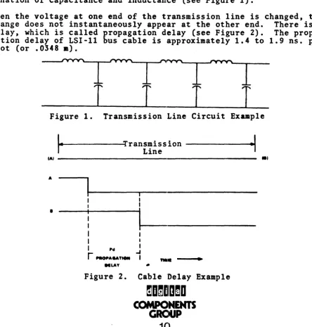
1.0 PROPAGATION DELAY
&
REFLECTIONSIf a voltage is supplied between any two conductors, they Ilay be con-sidered as a transmission line. The ideal transmission line input impedence looks like pure resistance but, in fact, is mainly a com-bination of capacitance and inductance (see Figure 1).
When the voltage at one end of the transmission line is changed, that change does not instantaneously appear at the other end. There is some delay, which is called propagation d.elay (see Figure 2). The propa-gation delay of LSI-II bus cable is approximately 1.4 to 1.9 ns. per foot (or .0348 a).
[image:14.618.73.518.284.749.2]I
I
I
I
Figure 1. Transmission Line Circuit Example
L
~~---~Transmission ---~.I
r
Line~I
-•
•
I I
I I
I I
I Pel
....
Ir
fI'ItOfI •••U'"
I"LAY •
•
Figure 2. Cable :Delay Example
mD~mlDmD
COMPONENTS
GRe ... P
1C)
)Jnote
NUMBER 012 PAGE 2 OFgA lossless transmission line of infinite length looks like a pure resistance of value Z • L/C. If such a line is broken and terminated with a resistor of this value (R • Z), the line will behave like an infinitely long line; i.e., appear resistive (see Figure 3). The impedence (Z) of LSI-II bus cable is approximately 120 ohms.
Z • 120U
.. cn ... MAT .... '
Figure 3. Cable Impedence Exaaple
When a voltage is applied to the line, the instantaneous power consumed will be:
P • E2/Z P • E2/120
Suppose now that the terminating resistor (R) is not equal to the characteristic impedence of the line. The power which is traveling down the line before 2it reaches the termination (during propagation delay) is equal to
E
IZ, but the power dissip!ted in the resistor after propagation delay is approximately equal to EIR.
If resistance (R) is greater than the impedence (Z), there will be
extra energy available at the termination and since energy cannot simply disappear, it will be reflected back int'o the line. After one more
propagation delay (for the return journey), this reflection will be seen back at the source (see Figure 4A).
ClOURCEI
CTERMINATIONI
Fi,ure I I
I
I
I
CAl
ell
I
I
' I I
I I I I
I I I
I I , I :
. . - N, ~ ... ...1.- ...
-+ ...
~ HI-.II I I I I
4. Iapedence Mismatch Example
j../note
NUMBER 012 PAGE 3 OF9Some of this reflection will be dissipated by the source impedence and some will be reflected back into the line. When this
re-reflection is seen at the termination (Figure 4B), (after still another propagation delay), the energy difference will be reflected back to the source. Eventually both source and termination will arrive at the same level. The important point to note here is that what was intended to be a level change with a clean, transition did not turn out that way on the line due to a termination mismatch between Rand
z.
Essentially the same situation oc,curs when the termination resistor is smaller than the characteristic impedence of the line. If resistance
(R) is less than impedence (Z), there will be a mismatch and this will also be reflected back to the source (see Figure 5).
ISOU.CEI-r
I I IfTE.MINATION) - _ _ ... Ii..-_. _ _ ....
ltd
Figure S. Iapedence (Low Resistance) Misaatch Example
Note that: (a) transmission line which is not terminated in its characteristic.impedence w~ll have refle~tions and (b) the voltage seen at any p01nt on the 11ne or at any 1nstant in time will be a combination of the incident and reflected voltage.
The amount of reflection depends on the mismatch, and approaches
100 percent for either a shorted or an open line (see Figure 6).
~II~DD~D
COMPONENTS
CiROUP
).Inote
.,
....
alfLECTION
1---:...--+--=:;;;;;;;...---.,
..
Figure 6. Misaatch Reflection Curve Exaaple
NUMBER 012 PAGE 4 OF9
Essentially the same thing happens on the negative going edge of a level change so that what seemed to be a clean transition as in Figure 7A may look aore like Figure 7B.
A.
..
Figure 7. Cable Mismatch (Waveform Example)
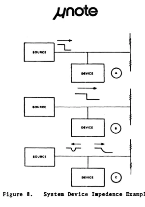
To further compound the problem, each device on the bus contributes its own unique impedence and mismatch in complex time relationships
(Figure 8).
[image:17.617.148.453.57.275.2]-...
r---"'\I
IOUtleE .1-.----'-r---t
L-C:
WCI0
-1--IOUtleE
C:"
CE0)
loutlet
Figure 8. System Devicn Iapedence Example
NUMBER 012 PAGE 5 OF 9
All of this impedence and resistance Ilismatch is normal and to be expected in LSI-II bus systems. The objective here is to point out the possible impedence mismatch and how to use the appropriate tools to minimize the effects of reflections and "noise".
1.1 LINE TERMINATION TECHNIQUE
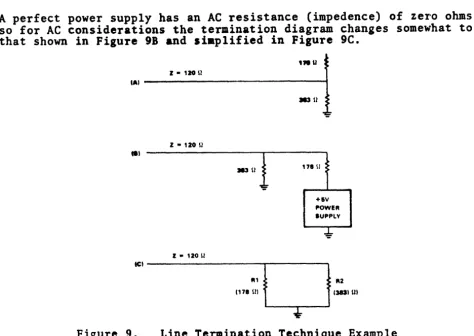
The question may be asked, how can a 178 and 383 ohm resistor properly termina te aline which has an impedenc:e of 120 ohms?
~D~DD!~D
COMPONENTS
CiROUI)
[image:18.618.134.430.53.475.2])Jnote
NUMBER 012PAGE 6 OF9
A perfect power supply has an AC resistance (impedence) of zey'o ohms, so for AC considerations the termination diagram changes somewhat to that shown in Figure 9B and siap1ified in Figure
ge.
z • 110 U
'N"
1
IAI
Jan
Z - 120 n
.1
.,u 1 " 1/
'oF
+IV
fI'OWER
IUPPLY
-=J:
1-12011
ICI
'm~,:
!
1,:'11"
[image:19.621.79.554.116.452.2]•
Figure 9. Line TeI11lination Technique Example
The choise of these two values satisfies both the quiescent condition and the required termination·impedence.
2.0 AC LOAD
An AC load is defined as a number related to the impedence that a bus element presents to an LSI-I1 bus signal line (due to backpla.ne wiring, PC etch runs, receiver input loading, and driver output loading).
This impedence load on a transmission line causes a "reflection" to occur when a step is sent down the line. This reflection shows up on an oscilloscope as a spike occurring shortly after an asserting or unasserting edge. An AC load is nominally 9.35 pf. of capacitance~
Nine lump~d AC loads reflect 20 percent and 20 lumped AC loads reflect 40 per.cent of a 2S ns. risetime step. AC loads must be distributed
NUMBER 012 PAGE 7 OF9
on the bus in the aanner described in the LSI-II Configuration Guidelines in order to provide bus operation with reflections guaranteed to be at or less than a tolerable level. The AC load rating of LSI-II bus elements is usually based on the greatest of the capacitances that the element :presents to the BDOUT, BDIN, BRPLY, BSYNC, BREF and BSACK signal lines. If the element is
customer-designed, its AC loadin~ lnust be determined from a reasonable estimate of the equivalent capac1tance presented to the LSI-II bus.
3.0 DC LOAD
A DC load is defined asa number related to the amount of DC leakage current that a bus element presents to an LSI-II bus signal line which is high (undriven). A DC load is nominally 105 uA (80 uA - receiver plus 25 uA - driver). However, the DC load rating of a bus element
is not strictly based on the element's signal line that has the greatest leakage, (e.g., DC leakage is less important on BDAL lines than it
is on BSYNC). The DC loading of an element should always be obtained from the specification for that element. It should not be obtained from a calculation of the receiver and driver leakage current, unless the element is custom-d.esigned and is not listed in the applicable documentation.
4.0
4.1
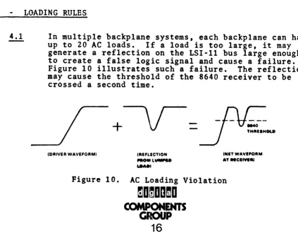
LOADING RULES
[image:20.613.94.517.417.747.2]In multiple backplane systems, each backplane can have up to 20 AC loads. If a load is too large, it may generate a reflection on the LSI-II bus large enough to create a false logic signal and cause a failure. Figure 10 illustrates such a failure. The reflection may cause the threshold of the 8640 receiver to be crossed a second time.
(DRIVER WAVEFORM) (REFLECTION
flllK)Wl LYMPeO
~I
(NET WAVI'ORM
AT . . CIIVI . .
Figure 10. AC Loading Violation
~DI~DD~D
COMPONENTS
C;~tOUP
).Inote
NUMBER 012 PAGE 8 OF 9To avoid this problem, some of the modules should be moved to another backplane. Best results will be
obtained when the AC loading of all backplanes is equal.
4.2 In single backplane systems, the number of AC loads.is limited by the bus termination impedence. The RC t1me constant of the loaded backplane determines the rise time of a signal line when a driver unasserts that line. If the maximum RC time constant is exceeded, the signal may not rise within 2S ns. (see Figure 11). 2S ns. is
the maximum delay permissible and still meet bus timing requirements.
(" Max. RC Time Constant
'Q! , ",'"
/ (71" ~
/ ,'~
/ "
Unacceptable RC Time Constant
Typical Backplane
Signal
/ /r:="'---
Receiver Threshold/
"
/, " /,,,,,
---"...-~
Max. Delay TimeFigure 11. Single Backplane Signal Waveform
To slow a rise time may also cause the output of some bus receivers to oscillate as the input signal rises through the receivers threshold.
5.0 DC LOADING RULE
The maximum number of DC loads in either a single or multiple backplane system is 20. If too many DC loads are put on the bus, the quiescent undriven voltage may be lowered to a level where bus receivers become
susceptible to reflections from lumped loads and the overall noise margin on the high end (bus undriven) may become too small.
6.0 CABLING RULES
)lnote
NUMBER 012PAGE 9 OF p
In multiple backplane systems, the c:ables must be at least 2 feet long. If a cable is less than 2 feet long, the system will behave like a
single backplane system.
In multiple backplane systems, the c:ables must be at least 4 feet different in length. When this rulE~ is violated and a driver in the middle backplane unasserts the bus, reflections from the other back-planes will arrive back at the middle backplane simultaneously and
superimpose. The net reflection may cross the 8640 threshold and cause a failure (see Figure 12). When thE~ cables are different lengths,
the reflections will arrive at slightly different times (see Figure 13).
\.
-
IO"'VE" WAVI .. O ....
Figure
DAIVE" WAVEfO . . .
+
I I---y--
+
----v-\. I '-~
-"IFLICTION "IFlECTION PM".NO NOM.NO
. , IU'IN "IU,OUT
Mau caeu
12. Violation Of Ca.ble Length
I
+
--v-
+
I I
----y-I
:"
"EFlECTION .. "OMINO 0' .U"N
CAeli
I
1'2
["UlECTION IJtHt".NO flW ev'OUT
.
~t
-ff--
I - - - I I N G T . . .- I
I
I
\.
Rule
\.
-
JNIT WAVI"O" .. A'A"ICTIO UIMHOLOAO
Waveform
NET WAVffO" .. ATU"fCTlO
~L"
•
)
'f/
Figure 13. Proper Cable Length Rule Waveform
~D~DDmD
COMPONENTS
GROUP
).Inote
NUMBER 013DATE
TITLE Installing APL-11 on 11V03 & 11T03 8
/2
17
DISTRIBUTION All APL-11 Customers PRODUCT
APL-11 ORIGINATOR Rich Bi1liS
PAGl oF!
When installing RT-11 APL on an 11V03 or 11T03 system, you must consider two options:
• Choice of:
SINGLE PRECISION variables (7 decimal d.igits of precision), OR
DOUBLE PRECISION variables (17 decimal digits of precision), AND
• KEV1l optional hardware
Unless the application requires high preclslon, we recommend choosing SINGLE PRECISION for speed reasons.
To choose the correct APL interpreter file for your configuration, refer to the following table:
KEVIl PRESENT?
YES
NO
SINGLE PRECISION
APL04.SAV
APLOO.SAV
~DmDD~D
DOUBLE PRB eI S I ON
APL03 .. SAV
NUMBER
).Inote
014
Correct Input Parameters for the
DATE
TITLE
QJV11
PROM Formatting Pr()gram 9/28
17
DISTRIBUTION All
QJV11
UsersPROijffili
ORIGINATOR Dave Schanin
PAGE 1 OF 2
The document that is shipped with the
QJV11
PROM Formatting Program has a serious error in it. The document is in the process of being corrected, but until such time, Chapter 7 of the Microcomputer Handbook should be used as a guide to using theQJVl1.
The error is in the description of the answers the user is supposed to give to questions printed by
QJV11.
A sample typeout is listed below:PROM V01·OO
ENTER AN OCTAL VALUE IN RESPONSE TO QUESTIONS WHICH REQUIRE A NUMERIC RESPONSE. TYPE 'Y' FOR YES AND 'N' OR NOTHING FOR NO. TERMINATE ALL RESPONSES WITH A <CR> (CARRIAGE RETURN). RUBOUT MAY BE USED TO DELETE ONE CHARACTER AT A TIME BEFORE <CR> IS TYPED. CTRL/U MAY BE USED TO DELETE THE ENTIRE RESPONSE. CTRl/O MAY BE TYPED TO TURN OFF OUTPUT TO THE TERMINAL.
HOW MANY WORDS ARE IN A PROM!' --.,;..::. HOW MANY BITS ARE IN A PROM WORO?_ HOW MANY PROMS ARE USED IN PI'RALLEL? _ ARE THE DATA BITS INVERTED? _
ARE THE ADDRESS LINES INVERTE[)? _ HOW MANY BYTES ARE IN THE AREP, TO BE OUTPUT? _
WHAT IS THE STARTING ADDRESS C)F THE AREA TO BE OUTPUT? _
IS YOUR INPUT/OUTPUT DEVICE ON THE HIGH SPEED READER/PUNCH? ....
READY INPUT, TYPE <CR> WHEN FtEADY. <~>
oo"yotJ WISH TO PUNCH TAPES? ,): DO YOU WANT TO VERIFY A TJ.PE? Y.
READY INPUT, .TYPE <CR> WHEN READY. <CB> DO YOU WANT A LIST OF THE PROM CONTENTS? Y DO YOU WANT iT ON A UNE PAINTER? ,!j
~D~mIDmD
COMPONENTS
CiRC ....
P2Ct
Initial Message
Input Parameters
j../note
NUMBER 014 PAGE 2 OF 2The proper responses, based on the type of PROMs used, are listed below. Note that all of this information is copied from the
Microcomputer Handbook.
h ... rneter
No. words ~n a PROM (N.)
No. bits in 8 PROM word (N s)
No. PROMs used in Pllrallel
Ale data bits inverted Ale addr. lines inverted How many bytes in the area to be output (N.)
Starting Address
1/0 device on the H.i.
Nader I punch
T... 7·5 QNl1 Input hrameters
MRVll-AA ~ons
512 X 4 PROMs 256 X 4 PROM.
1000 400
4 4
4 4
N N
Y Y
20000 10000 0. 20000. 40000. 0. 10000. 20000. 60000. 100000, 30000, 40000,
etc. etc.
YorN
~D~DDmD
YorN
MRVU-BA Applbtions
lK X 8 PROMs
2000 10
2
N N
20000
0. 20000, 40000, 60000, 100000,
etc.
).Inote
NUMBER 015DATE
TITLE Power Sequencing for the KD11-HA Module 11 / 21 /77
DISTRIBUTION Unrestricted PRODUCT
KD11-HA ORIGINATOR Dave Schanin
PAGE 1 OF 3
The KD11-HA power-up and power-down sequencing functions are exactly the same as on the KD11-F. The user may select anyone of four power-up modes:
Mode Start-up Function
o
PC at 24, PS at 26 1 OOT microcode 2 PC at 1730003 Reserved microcode
Power-Up
On all KOl11
s, there are two methods (not modes) to start the LSI-II and cause it to power-up through the selected mode:
Method 1: Use an H780 power supply or KPV11 power sequence module. They function as follows::
a) DC power is applied to the backplane, while BPOK and BOCOK are asserted.
b) 3-10 ms. following DC power application, BOCOK is released. At this time, the CPU comes up, does a fast DIN on location 4 (a DIN which ignores the actual contents of location 4), and in doing so reads the power-up jumpers and the state of BPOK. The CPU senses BPOK is asserted and continues looping.
c) 70 ms. (min.) followi'ng the release of BDCOK, BPOK is released. The CPU, which had been looping on reading the BPOK linE!, now senses that BPOK has been released and jumps to the location specified by the power-up jumpe!rs.
~D~DD~D
COMPONIENTS
GROUP
)lnote
NUMBER015 PAGE2 O!Method 2: Use a pushbutton. Connect a pushbutton, preferably debounced, to the BOCOK line. This pushbutton should allow BOCOK to float when the button is released, and should assert (ground) BOCOK when the button is depressed. This method functions as follows:
Power-Down
a) DC power is applied. BOCOK and BPOK are released. The CPU is in an undefined state and will not run.
b) The pushbutton is depressed following DC power application and, therefore, BOCOK is asserted. As long as BOCOK is asserted, the CPU is in a reset condition and non-functional.
c) The button is released so BOCOK is released. The CPU comes up, does a fast DIN on location 4, reads the power-up jumpers, and the state of BPOK.
d) Since BPOK is not asserted, the CPU jumps to the location specified by the power-up jumpers.
On all K011's, two power-down methods exist:
Method 1: Power-fail detection. This requires a KPV11 or an
H780 power supply. This method allows for detection of AC loss by causing a trap through location 24. The CPU then has 4 ms. to complete its transaction and halt. This method works as follows:
a) Upon AC loss, BPOK is asserted. This causes a trap through location 24. The power supply ride-through will maintain DC power for 4.05 ms. (min.) beyond AC power loss. The user software must complete a'll housekeeping functions in less than 4 ms. and halt.
b) 4 ms. following BPOK assertion, BDCOK is asserted suspending CPU operations, locking out core memory access, and initializing peripherals.
c) 5 us. following BOCOK assertion, DC power is lost.
Method 2: Non power-fail detection. Loss of DC power, while BOCOK and BPOK are released. Under this method, DC power is simply shut off to the backplane. The CPU may lose power anywhere in a bus or execution cycle and may cause any random event to occur on the bus or at a peripheral due to the unknown state of all devices on the bus as they
j../note
NUMBER015PAGE3 AS:
randomly lose power. This is unacceptable in a core-based system since the core contents may get "scrambled".
However, in a MOS RAM system where the peripherals cannot cause damage Olr harm to anythi ng shoul d they execute a random operation, this power-down method is perfectly acceptable.
How do these power-up and power-down ml~thods affect the new KDII-HA? For most applications, the only requirement is automatic power-up and -down, as outlined in Method 2. Full sequencl~d power-up and -down, Method 1, is usually only required for core based systems. Therefore, the KDII-HA incorporates a "wake-up" circuit which automatically powers up and down the CPU according to Method 2 (i.e., no power-fail detection) with no external hardware requirements. Essentially, the "wake-up" circuit con-sists of a single shot tied to the BDCOK line which is asserted following the application of +5 volts backplane !power. Since this single shot only is tied to +5, +5 and +12 must come up within 50 ms. of each other to insure reliable power-up. See Micro Note #016 for recommended power supplies.
CAUTION: MSVII-B memories should not be used as bank 0 memory on the KDII-HA unless it is ECO REV E or higher. Failure to use at least a REV E board will result in inability of the KDII-HA to power-up (note that external refresh is required from the REVll). The reason for this is that on REV D or lower MSVII-B ' s, the negative voltage charge pump will not attain operating voltage before the KDII-HA does a fast DIN on location 4 to read the power-up jumpers. If location 4 does not reply, the CPU will hang, and never power-up.
~D~IJD~D
COMPC ..
ENTS
CRC)UP
).Inote
NUMBER 017 DATETITLE LSI-11/2 Processor Clock 11 /28 /77
DISTRIBUTION Unrestricted PRODUCT
ORIGINATOR Ron Young KD11-HA
PAGE 1 OF1
The CPU clock is a crystal controlled (non-adjustable) clock that will set the machine cycle time to 380 ns. + .01%. This should, at last, lay to rest any competitor's claim that we have to "tune" the clock to make the CPU work.
The tight tolerance on the clock will serve to tighten system performance between systems.
In addition, the 380 ns. figure was selected to optimize CPU--memory performance for our new memory offering without impairing performance with our older memories. This marriage of CPU and memory will serve to further enhance system performance.
NOTE: It has been brought to my attention that customers have been using "instruction loops" for timing purposes. This is not a good method for marking time. One must consider that the memory has "refresh cycles" to perform which can add time to the
instruction execution time. This makes exact execution time impossible to calculate.
).Inote
NUMBER 018DATE
TITLE DR11-C vs. DRV11 11 / 28 / 77
DISTRIBUTION Unrestricted PRODUCT
DRV11 ORIGINATOR Ron Young
I PAGE 1 OF 4
The following tables and figures 1 ist thle differences between the DR11-C and the DRV11.
Some concern has been expresses on the mlnipulation of the REQUEST A and REQUEST B lines. Let me remind you of the IIhandshakingll necessary between the interface and the user's device. The user's manuals (DR11-C General Device Interface Manual--chapter 6, and ADVI1-A, KWV11-A,
AAVII-A, DRVII User's Manual--chapter 5) state the need for the user to hold the REQUEST lines until the NEW DATj~ READY or the DATA TRANSMITTED signals are generated. The recol11l1ended method is illustrated in Figure 1 below.
ruSE~sD~;c;-
- ,
LOGIC
CONN No. ,
OR-3 HEW DATA READY H
ivvr---~
: OR-3 REOUEST A H
SET REO A L
REOUEST
A
o
~~~~---~---~
DR It -C INTERFACE
(M11601
CONN No.2
r - - DR-3 DATA TRANSMITTED H
: c - - - + - 1
I I
! S OR·3 "fQUfST 8 H
L __
SET REO 8 L
R~OUEST
8
o
L _______ J
~D~Dlm~D
COMPOI~EMTSGROUP
SIGNAL
New Data Ready
Data Transmitted
Init.
New Data Ready LO* (byte)
New Data Ready HI* (byte)
All Other Outputs
).Inote
TABLE I
OUTPUT SIGNAL LOADING
DRVll
10 Loads
**
30 Loads
10 Loads Per Connector
N/A
N/A
5 Loads
NUMBER 018 PAGE2 OF 4
DRII-C
-30 Loads
30 Loads
30 Loads Over Both Connectors
30 Loads
30 Loads
7 Loads
*
Byte-oriented control signals available on DR11-C only. ETCH REV E or later.**
One load is defined as (-1.6 rnA) one TTL loadEXTERNAL CAPACITOR
None
470 pF.
820 pF.
None
00047 uF.
• 01 uFo
• 02 uFo
• 03 uF.
TABLE II
VARIABLE LENGTHS OF OUTPUT CONTROL SIGNALS
NEW DATA READY
OR11-C
-350 ns.
500 ns.
600 ns.
DR.Vll
350 ns.
750 ns.
15501 ns.
23301 ns.
31501 ns.
~D~DDmD
COMJtONENTS
GROUP
28
NUMBER 018
PAGE 3 OF l1
DATA TRANSMITTED
DR11-C
450 ns.
600 ns.
750 ns.
DRV11
350 ns.
750 ns .
1550 ns .
2330 ns .
)Jnote
TABLE III
BERG CONNECTOR PIN DIFFERENCES
SIGNAL
In 02
Out 02
New Data Ready HI (Byte)
New Data Ready LO (Byte)
DRV11
J2 H,E
J1 RR,NN
N/A
N/A
~D~DDmD
COMPONENTS
NUMBER 018
PAGE 4 OF 4
DR11-C
J2 H
J2 NN
J1 E
NUMBER
).Inote
019DATE
TITLE EIA RS-422 and RS-423 11 /29 /77
DISTRIBUTION Unrestricted PRODUCT
DLV11-J ORIGINATOR Ted SemQle
PAGEl OF4
Electronic Industries Association (EIA) standards RS-422 and RS-423 have been accepted as new international standards for transmission lines between electronic equipment. These new standards offer a considerable performance improvement over traditional EIA RS-232C and current loops. Unlike RS-422 and RS-423 which were developed so that newly designed equipment could have higher performance, RS-232C and current loops grew out of existing applications and were accepted after the fact as standards. RS-232C was originally developed by the Bell System as a standard for interconnecting terminal equipment to communications equipment (modems). Current loops were the method employed to inter-connect teletypewriter devices.
Figure I graphically shows the performance differences between RS-232C, RS-422 and RS-423. With RS-232C, the maximum reliable cable length is 50 feet and the maximum frequency is 20K baud. Comparing that with RS-422, you will see that RS-422 has the capability of going all the way up to 4000 feet and a maximum baud rate of 10 megabaud (although not simultaneously). Table I is a more detailed comparison of the
specifications.
The new RS-422 and RS-423 specifications define the characteristics of the transmitters and receivers used to drive the transmission line as well as the characteristics of the transmission line itself. The
receivers and cables used for both standards are identical, but the transmitters are different. RS-422 is a differential (balanced) line system which is capable of transmitting data at high baud rates over long distances with the high noise immunity associated with balanced line systems. RS-423 is a single-ended line system which inherently does not have the capability of a differential line.
EIA RS-423 is actually a stepping stone between EIA standards RS-232C and RS-422. RS-423 transmitters and receivers are actually backward compatible with RS-232C transmitters and receivers. This means that an RS-232C
transmitter can send data to an RS-423 receiver and vice versa. Since the receivers used for RS-423 are identical to the receivers used for RS-422, it is possible to design systems which will work with existing RS-232C equipment and can then be upgradted (usually via a strapping
change) to RS-422. This provides for a smooth transition between current equipment utilizing RS-232C and newly designed equipment utilizing
~D~DDmD
COMPOMENTS
).Inote
NU~t1BER 019 PAGE 2 OF4RS-422 without instantaneously obsoleting existing equipment. Remember that when RS-232C and RS-423 transmitters and receivers are interconnected, the system performance is that of RS-232C rather than the improved
performance of complete RS-423 systems.
The DlVI1-J 4-line serial line unit has been designed with the new hardware for RS-422 and RS-423. Straps have been provided which permit use of the RS-423 transmitters initially and then by restrapping, the board can be upgraded to RS-422 transmitters. The DLVI1-J can, therefore, be used with RS-232C peripheral devices. In the future, new peripheral devices designed by Digital and other manufacturers will most likely utilize the new RS-422 specifications. The maximum baud rate with the DLVI1-J is 38.4K baud, not the limit of either RS-422 or RS-423.
The product line has additional technical details on RS-422 and RS-423 for those who need it.
10K
I
-4K
LLI LLI u...
:I:
l - 1K
e.!' Z
LLI ...J LLI ...J
co
c::c u
100
~8
10 100
j../note
RS-2 2C
1K 10K 20K lOOK
DATA RATE - BAUDS
FIGURE 1 - DATA RATE
vs.
CABLE LENGTH~D~DD!~D
COMPONENTS
GROIII»
32
1M
NUMBER 019 PAGE 30F 4
).Inote
NUMBER 019 PAGE 4 OF 4Table 1. Comparison of the old and new interface standards
Parameter
Line length (recom-mended max-may be exceeded with proper design).
Input Z
--Max frequency (baud)
Transition time>l< (time in undefined area between "1" and "0") tr = 10 to 90%
dV/dt (wave shaping)
Mark (Data "I") Space (Data "0")
Common mode voltage (for balanced receiver)
Output Z
f---Open-circuit output voltage (V 0>
Vt = loaded V 0
Short circuit current
Power-off lea kage (V 0 applied to unpowered
device)
Min receiver input for proper Vo
r I~ bit perrod
.. across output. or output to ground t whichever IS greater
RS232 RS422
-50 ft 1200 m (4000ft) See Fig. 3
3 to 7 kQ > 4 kQ 2500 pF
20kbaud 10 Mbaud
4% of T tr ~ 0.1 T:
or T ~ 200 ns
1 ms tr ~ 20 ns:
T < 200 ns
30 V/p.s See transition
time
-3 V A < 8 +3 V A > 8
- -7 V < VCM < +7 V
- < 100 n Balanced 3 V < I Vo I < 25 V IVo I~ 6Vu 5<IV o l<15V 2Vor.5Vo< IVt It
3 to 7kU load 100 n balanced load
500 mA 150 mA
> 300 Q < 100 ,.,.A
2 V < I V
8
I < 25 V o V <eVo < 6 V Vo applie Vo applied> ±3 V 200 mV differential
EI H'TRONI( DI SHiN IK. Scplcmhcr I. 1977
~D~DD~D
RS423
1200m (4000 ft) See Fig. 5
> 4 kQ
-100 kbaud
tr ~ .3 T: T < 1 ms
tr ~ 300 p.s:
T > 1 ms
See Fig. 4
-A = Negative 8 = Positive
-< 50 12
4V~ IVol~6V
IVt I ~ .9 IVI)!
450 U load
150 mA
< 100 p.A I Vol < 6 V Vo applied
[image:37.612.59.542.146.529.2]NUMBER
),Inote
020DATE TITLE 9x6 Slot Backplane Documentation Error 11 /30
DISTRIBUTION DDV11-B Users PRODUCT
DDV11-B ORIGINATOR Joe Austin
PAGE 1 OF1
There is an error in the two documents which define the backplane pin assignments for the DDV11-B 9x6 slot backplane. Pins ET1 and FT1 in
all slots are actually bussed to ground as shown in the table below.
These pins are not blank as indicated in the Components Group, Logic Products Option Bulletin (ED 06703 76, dated September, 1976) entitled tlDDV11-B 9x6 Slot LSI-II Backplane tl,
(Correcte:d)
DDV11-B Backpllane Pin AssIgnments
/7
SIDE 2 1 2 2 1 2 1
ROW A&C A&C B&D
A +5V BSPARE 1 +5V B -12V BSPARE 2 -12V
C GND BAD16 GND D +12V BAD17 +12V E BDOUTL SSPARE 1 BDAL2L
F BRPLY L SSPARE 2 BDAL 3 L H BDINL SSPARE 3 BDAL 4 L
J BSYNCL GND BDAL 5 L
K BWTBTL MSPAREA BDAL6L L BIRQL MSPAREA BDAL 7L M BIAKIL GND BDAL8L N BIAKO L BDMRL BDAL9L P BBS7L BHALT L BDAL 10 L R BDMG I L BREFL BDAL 11 L
S BDMGOL PSPARE 3 BDAL 12 L T BINITL GND BDAL 13 L U BDALOL PSPARE 1 BDAL 14 L V BDAL 1 L +58 BDAL 1-5 L
B&D BDCOKH BPOKH SSPARE4 SSPARE5 SSPARE6 SSPARE 7 SSPARE 8 GND MSPARE B MSPARE B GND BSACK L BSPARE6 BEVNT L PSPARE 4 GND PSPARE 2 +5B
~D~DD~D
COMPC)NENTS
Ci~:xIP3:4
E +5V -12V GND BLANK BLANK BLANK BLANK BLANK BLANK BLANK BLANK BLANK BLANK BLANK BLANK BLAN BLAN BLANKE F F
BLANK +5V BLANK BLANK -12V BLANK BLANK GND BLANK BLANK BLANK BLANK BLANK BLANK BLANK BLANK BLANK BLANK BLANK BLANK BLANK BLANK BLANK BLANK BLANK BLANK BLANK BLANK BLANK BLANK BLANK BLANK BLANK BLANK BLANK BLANK BLANK BLANK BLANK
LANK~ LANK BLA
LANK gnd BLANK
NUMBER
).Inote
021DATE
TITLE Comparison of Data Transmission Techniques 12 / OS
DISTRIBUTION Unrestricted PRODUCT
---ORIGINATOR Ted Semple
PAGEl OFS
Frequently, the application artses where a data transmission path has to be established between two devices. Usually the distance between the devices is known, and also the rate of data transmission is known. The problem comes with deciding which is the best communication technique to use to interconnect the devices. Figure I should help you with this decision.
Figure I is a graph of data rate vs. distance for the various standard transmission techniques. Parallel data transmission techniques (PLU's and DMA) give the highest data rate; however, they are only good for relatively short distances. The serial techniques (RS-232C, RS-422 and current loops) are good for longer distances but at limited data rates.
While analyzing Figure I, remember that the axes are logrithmic and that the data rate is in words per second rather than baud rate. The limits established for both distance and data rate are a function of both the inherent limitations of the transmission technique and of the Digital Equipment Corporation device used to do the interconnection. As an example, look at the 422 section of the graph. Maximum distance is 4000 feet as established by the EIA standard RS-422, but the maximum data rate of 1920 words per second is based on the maximum baud rate of the DLV1I-J which is 38.4K baud.
Table I is a summary of the LSI-II devices which can be used with each communication technique. The Unibus equivalent for each device is also shown. Currently, there is no Unibus device for EIA RS-422.
The material for this Micro Note was extracted from the "CPU Inter-connection Techniques" session given at the DCG International Sales Meeting. The entire presentation is available in 3S mm. slides, together with backup material, from the LSI-II Presentation Library. Contact the product line if you would like further information.
~D~DD~D
lOOK
10K
t-u.
I lK
I
L&J
U Z
~
t-V')
...
CI
100
10
1
EIA RS-232C
w/Modem EIA
).Inote
FI~iURE I
DATA RATE vs. DISTANCE With Digital Devices
4K
1.5K RS-422
EIA RS-423
Current Loop
EIA RS-232C
ALL TECHNIQUES
480
10 100 1K
1920
DMA (3 - STATE)
PLU
10K
DATA RATE Words/Sec.
~DI~DDmD
COMJaoMENTS
GROUP
36
-DMA (TTL)
46K lOOK
- 50
- 15
1M
NUMBER 021
)./note
NOTES AND ASSUMPTIONS FOR FIGURE 1
1. Data Rate Definition
a. One word equals 16 bits
NUMBER 021
PAGE 3 OF f
b. For serial techniques, one word equals two characters formatted with one start bit, eight data bits and one stop bit. Asynch-ronous serial transmission is assumed.
2. Serial Line Maximum Data Rate
a. Modems were limited to 120 words/sec. (2400 baud) because modems with higher rates cost more than LSI~11 systems usually warrant. Higher data rate modems are generally synchronous rather than asynchronous.
b. 480 words/sec. is equal to 9600 baud, the limit of the DLVll SLUe
c. 1920 words/sec. is equal to 38.4K baud, the limit of the DLVII-J SLUe
3. PLU (Parallel Line Unit) Limits
a. The TTL inputs/outputs of the DRVll limit the distance to 15 feet.
b. 46K words/sec. assumes non-interrupt driven program servicing with bit testing (TSTB, BMI, MOV and SOB). 97K words/sec.
is maximum rate with program servicing without bit testing (MOV and BR). With interrupt driven servicing, the maximum limit is 20K words/sec. assuming 50 us. for interrupt latency and software servicing of interrupt. (380 ns. CPU
microcycle time)
4. DMA (Direct Memory Access) Limits
a. The DRVII-B can be used up to 50 feet because it has tri-state drivers and receivers. The distance is limited to 15 feet with TTL devices like the DRII-B.
j../note
b. OMA transfers with the ORVII-B and the ORII-8 are limited
NUMBER 021 PAGE 4 OF5
to SOOK words/sec. in burst mode operation. 250K words/sec. is the limit for single cycle mode operation with either devi ce. These 1 imi ts are dev1i ce dependent; they are not LSI-II bus limits (which is 8:~3K words/sec.). Remember that burst mode can disrupt mE~mory refreshing if bus refreshing (OMA or microcode) is used. Self-refreshing memories, MSVII-CO or MSVII-0" eliminate this problem.
~DmD[I~D
COMPC»IENTS
Loop
EIA (RS-232C)
EIA W/Modem
RS-422
PLU
DMA
)./note
TABLE I
DEVICES
LSI-II
DLVII
DLVII
DLVII-E
DLVII-J
DRVII
DRVII-B
mD~DDmD
PDP-II
DLII-C
DLII-0
DLII-E
DRII-C
ORII-B
NUMBEH 021
NUMBER
)lnote
023DATE
TITLE Using the MSVII-0 30K OEtion 12 /16 /77
OISTRIBUTION Unrestricted PRODUCT
MSVII-0 ORIGINATOR Rich Billig
PAGE 1 OFI
The MSVI1-D memory, when configured with the full complement of 16K RAM chips, provides 32K words of storagE~. In the LSI-II memory map, however, the top 4K words (addresses 160000 to 177777) are normally reserved for I/O device registers (the so-called "I/O Page").
The 32K MSVII-0, as delivered, operates as a 28K word memory for the LSI-II. In this configuration, it is totally compatible with all DEC-supplied software. The 4K word reg~ion which is located at address 160000 is present but inaccessible to the program.
To allow more of the memory to be used (for large applications), a jumper-selectable option on the MSVII-0 makes 30K words (rather than 28K) addressable by the program. This "is done by "removing" the low 2K word area of the I/O page (addresses 160000 to 167777). When the 30K option is enabled, the memory map is:
000000 to 167777
170000 to 177777
RAM '~emory
I/O Page
Because current system software expects a 4K word I/O page, RT-11 and RSX-11S cannot make use of the extra 2K words of RAM. (A
user-written program operating under either system may, however, access locations 160000 to 167777 directly if desired.)
Engineering is presently evaluating the feasibility of supporting the full 30K RAM in the next release of RT-ll (V3B). Similar modi-fications to RSX-I1S would be more extensive and are not currently planned.
When the 30K option is used, all I/O devices must be Configured to place their I/O page addresses in the range 170000 to 177777. (This would not be the default assignment for such devices as the DUV11 and DZVll.) Also, it is not possible to use the REV11 bootstrap with this option, as a portion of the bootstrap PROM code resides at
addresses 165000 to 165777. The new quad bootstrap module (BDV11) may be used in the 30K environment.
~D~DD~D
COMPOIt-tENTS
GROUP
)lnote
NUMBER 024A SUPERSEDES pNOTE #024DATE
TITLE Async., Serial Line Unit Comparisons 10 / 13 / 78
DISTRIBUTION LSI-II Users PRODUCT
Async. SLU's ORIGINATOR Joe Austin
PAGE 1 OF
Attached are charts comparing the different members of the families of asynchronous serial line products. All modules of the DLV11 series are dual height modules. The DLV11-E, -F, and -J modules detect overrun conditions which are reported in the receiver CSR. These modules will not generate phantom interrupts on overrun.
DLV11-J
5
Each of the 4 serial ports on this module are separate and independent from the others. This is not a multiplexed module. Each port has its own CSR's, data buffers, interrupt vectors, baud rates, UARTs, etc. The net effect of this module is to achieve a 4:1 compression ratio over the DLV11-F and the DLV11. The main functional difference between the ports of the DLV11-J and the DLV11 is that the DLV11-J provides the higher performance EIA RS-422 and RS-423 interfaces (RS-423 on the DLV11-J also meets the EIA RS-232C specification) and requires the DLV11-KA option
(one per port) to add the 20 mA current loop interface, to add 110 baud, and to add reader run functions.
DLV11-E
This module is functionally equivalent to the DL11-E except that it has programmable transmit baud rates. This module provides one serial port that has full modem control.
DLV11-F
This module is functionally equivalent to the DLV11 and will eventually replace it. In addition, it can be configured to provide programmable transmit baud rates.
DLV11-KA
Thfs option allows an EIA port to be connected to a terminal with a 20 mA interface, such as an ASR33. It consists of a small PC card containing the interface conversion logic within a box that is externally mounted. Mating cables are included. This module is not restricted to 110 baud.
).Inote
TABLE 1
-COMPARISON OF HARDWARE FEATURES
Number of Ports Per Module EIA RS-232C
Full Modem Control Limited Modem Interface EIA RS-422, RS-423
Data Leads Only 20 mA Current Loop
RCVR Active or Passive XMIT Active or Passive XMIT Active Only
CCITT
HALT on Framing Error (4) BOOT on Framing Error (4) Baud Rates (see Table 3)
Programmable
Split Speed Clocks Included Reader Run Control
Error Flags
Transmit Break Generation Bit Receiver Active Bit
Maintenance Bit
Internal Real Time Clock UART Cleared by INIT UART Cleared by DCOK No Trap on Write to Input
Buffer Easy Configuration Using
Wire-Wrap Jumpers Stop Bits
1 1.5
2
ur
IBI Sc:C c:C CQ U Q I I I I I
... ... ... ... ... ... ... ... ... ...
N - I - I - I - I
Q Q Q Q Q
8 1 1 1 1
.; .; .; .; .; .; .; .; .; .; .; .; .; .; .; .; .; .; .; .; .; .; .; .; .; .; .; .; .; .; .; .; .; .; .; .; .; .; .; .; .; .; .; .; .; .; .; .; .; .; .; .; .; .; .;
~DmIODmD
COMPCNNTS
CiRC)Up
4:2
LLJ 3:
I I
... ... ... ...
- I - I
Q Q
1 1
.; .; .; .; .; .; .; .; .; .; .; .; .; .; .; .; .; .; .; .;
LS -1
LLJ LL.
... I I ... ... ... :::- ... ...
- I :::-
:::-Q - I - I
Q Q
1 1 1
.; .; .; .; .; .; .; .; .; .; .; .; .; .; .; .; .; .; .; .; .; .; .; .; .; .;
~3) .; .;
.; .;
.;
.; .;
.; .;
.; .; .;
.; 5) 5)
NUMBER 024A
PAGE 2 OF 5
l B)S
CQ
r-:> ~
..
I c:C
... I I ... ... ...
:::- ... ...
- I :::-
:::-Q - I N
Q Q
4 1 4
.;
.;
.;
.;
2) .;
2) .;
.;
6) 6)
.;
2) .;
.; .;
.; .;
3) .;