for 3-D Integrated Circuits. (Under the direction of Professor Paul D. Franzon.).
In traditional design of power delivery networks (PDNs), the impedance property of the network is required to be less than the target impedance across a broad range of frequencies to ensure IR-drop is minimized and simultaneous switching noise (SSN) is suppressed. It is becoming increasingly more challenging to meet the electrical constraints and performance of modern integrated circuit (IC) design using conventional interconnect technology. However, three-dimensional (3-D) stacking using through-silicon via (TSV) technology has emerged as a viable solution to reduce interconnect delay, power supply noise and achieve heterogeneous IC module integration. A major advantage to using TSVs is the shortened interconnect path to pass data signals and deliver clean power at a fast rate between chips. A low impedance return path in the PDN guarantees negligible interference or noise into other sensitive timing and signaling circuits (e.g. signal generation circuits and PLLs). In an effort to keep up with scaling technology and robust PDN designs, TSV technology is a promising option relative to the other interconnect options available today.
by Gary Charles
A dissertation submitted to the Graduate Faculty of North Carolina State University
in partial fulfillment of the requirements for the degree of
Doctor of Philosophy
Electrical Engineering
Raleigh, North Carolina 2015
APPROVED BY:
_______________________________ _______________________________ Dr. Paul D. Franzon Dr. Winser E. Alexander
Committee Chair
DEDICATION
I dedicate my dissertation to my family.
My mother Annalia “Maya” Charles most amazing woman in my life; love you always for your strength, wisdom, humility and grit.
To my older siblings,
Jocelyn, Dieune, Nicole, Armand and Abraham, and my younger siblings,
Diana and Gertrude.
BIOGRAPHY
Gary Charles was born in Miami, Florida to Haitian parents Dicelien Simeon and Annalia Charles. He grew-up attending primary school in the heart of the city downtown Miami. As a young teenager, he was accepted into an engineering magnet program called Florida Action for Minorities in Engineering (FL.A.M.E). He was exposed to an array of college engineering courses as a high school senior which afforded him an early exposure to university life. After receiving his high school diploma, Gary attended Florida International University for his undergraduate studies and received a Bachelor’s of Science in Electrical Engineering. Immediately after receiving his B.S., Gary was accepted into the Electrical and Computer Engineering Master of Science program at North Carolina State University located in downtown Raleigh, North Carolina. He successfully completed his M.S. in Electrical Engineering and continued at North Carolina State for the doctoral program. Gary is a member of the Microelectronics Systems Laboratory (MSL) group where his research interest focused on the design, model and characterization of power delivery systems, on-chip interconnect structures and 3-D IC architecture.
ACKNOWLEDGMENTS
Although the doctoral journey is an individual odyssey and at times considered a labyrinth, I could never have reached the heights or explored the depths without the support, guidance, help and prayers of a lot of amazing people. First and foremost, I would like to acknowledge and thank God for protecting me and sustaining my health enabling me to witness this moment. Next, I would like to thank the great intellectual venture capitalists known as my research committee. Dr. Paul D. Franzon, the chair of the committee, many thanks for the invaluable investment of your time, your guidance, your ideas and most importantly your patience to see me get through the rough patches of this dissertation journey. Dr. Winser Alexander, I appreciate everything you’ve been able to do for me that ranges from advices on how to handle various situations to your unwavering support and words of encouragement. Dr. Rhett Davis, thank you for your help, your time, your valuable suggestions and research perspectives. Dr. Amassa Fauntleroy, I appreciate you making yourself available whenever I needed you, thank you.
I am incredibly indebted to several past and present individuals in the ECE dept. and Graduate School who provided countless administrative help, spoke on my behalf when teaching assistant positions became available and helped alleviate the financial burden by notifying me of grant money when they were available. Thanks to Julibeth ‘JB’ Briseno your ‘little Taye’ did it, Pascale Toussaint, Ms. Elaine Hardin for the motherly advices and constant reminders to register on time to avoid late fees. Thanks to Dr. Devetsikiotis, Dr. Brian Hughes, Dr. Hatice Ozturk, Dr. Snyder, Dr. Trussell, Dr. Barlage, and Dr. Lazzi. In the Graduate School, I will forever be thankful to Dr. David Shafer for the tremendous support dating back to the days of the MGE program. Dr. Mike Carter for the constant push, pep talks to get it done, and Dr. Sutton for being there to listen to my sorrows, frustrations, and moments of triumph.
thanks go to the Parkers for allowing me to be a part of their beautiful family. Thanks to the following families and friends I’ve made in North Carolina: the Taylors, the Adams, Sister Emelda Lewis, Sis. Stoval, Wesner ‘Shoopy’ Joseph family, Pastor Johnson and his family, John and Raquel Fleming, Michael Robinson, Shameeka Scott, Niambi Hall-Campbell, Bola, Ninrat Datiri, Jeenly Lewis, Nehemiah Mabry, Mustafa ‘Berke’ Yelten, Daniel Schinke, Shep, Miao, Ravi Jenkal, Chanyoun, Hoon-Seok, Senanu Ocloo, YoungSoo, Ramsey Hourani, Matthew Craver, Thorlindur, Ting Zhu and Peter Gadfort.
I would like to acknowledge very close friends and strong supporters from back home: Lourder, Ty, Sonny, Pastor Demetrius and his family, past and current JCOG members, Deacon Blaize and his family, the entire South Miami members I love you all so much. In addition, to my close friends in Arizona: Demetrius Mosley, Robert Crosby, Brook Berhane, and Emeka Ojeh. Finally, two close friends of mine in California I would like to acknowledge: Guy Nesbitt and Cardin ‘Leo’ Campbell thanks for having my back brothers.
I would like to acknowledge several individuals who I have come to know and love dearly who unfortunately are no longer with us. Colette Blaize, Tilly and Derrick Person were individuals who consistently reminded me to focus on accomplishing my goals, to keep the Sabbath and to make God the vanguard of major decisions. I accomplished this goal with you in mind.
Last and most certainly not least, thank you from the depths of my heart to my huge family of cousins, nieces, nephews, aunts, uncles, in-laws too many to name, thank you for your prayers and many years of support. I hope that I serve to be the positive role model and beacon of inspiration to you all. You also have it in you to reach your goals and dreams; go be great. Individuals I fail to name, you made this moment a reality as well, thank you. Gary Charles
August, 17th 2012
TABLE OF CONTENTS
LIST OF TABLES ... vii
LIST OF FIGURES ... viii
TERMS AND ABBREVIATIONS ... xi
CHAPTER I: Introduction...1
1.1 Motivation and Overview ... 1
1.2 Power Delivery Challenges in 3-D IC ... 4
1.3 Research Objectives ... 7
1.4 Overview of Dissertation Chapters ... 9
CHAPTER II: Interconnect Background and TSV Technology ... 11
2.1 Literature Review of On-Chip Interconnects for Power Delivery ... 11
2.2 Background of Through Silicon Via (TSV) Technology ... 19
2.3 TSV Benefits ... 20
2.3.1 Performance ... 20
2.3.2 Form-Factor ... 21
2.3.3 Scalability ... 22
2.3.4 Interconnect Power Reduction ... 22
2.4 Electrical Modeling of TSV ... 23
CHAPTER III: Parametric Modeling of On-Chip Interconnects ... 31
3.1 Back-End of Line (BEOL) Power Grid Structures ... 31
3.2 Power/Ground TSV interconnect pairs ... 40
3.3 Model and Characterization of Other On-Chip Interconnects ... 52
3.4 Analytical Impedance Models and Segmentation Method ... 55
CHAPTER IV: Case-Study: Various TSV-Based PDN Stacking Topologies ... 60
4.1 On-Chip Stacking Topologies: Face-to-Face (F2F), Face-to-Back (F2B) and Back-to-Back (B2B) ... 61
4.2 On-Chip Decoupling Solution for TSV-based PDNs ... 66
4.2.1 Modeling MOS decoupling capacitors ... 67
4.2.2 Modeling MIM decoupling capacitors ... 69
4.3 Case-Study: Impedance of Various TSV-based PDN Topologies ... 73
4.4 Power Supply noise of TSV-based PDN ... 82
CHAPTER V: Concluding Remarks & Future Works ... 89
BIBLIOGRAPHY ... 92
APPENDICES ... 101
LIST OF TABLES
Table 1-1: Intel Microprocessor Trends of last decade ... 4
Table 1-2: Shows a design challenge roadmap for 3-D integration technology ...5
Table 1-3: Emerging Global Interconnect Level Roadmap for TSVs ...6
Table 1-4: Emerging Intermediate Interconnect Level Roadmap for TSVs ...6
Table 2-1: Summary of Electrical Properties for Wire Bond vs. Solder Bump ...15
Table 2-2: Comparison of TSVs and current interconnect options ...16
Table 2-3: Monolithic 3D-IC versus 2D-IC using similar technology node ...21
Table 3-1: Value of Interconnect components of a unit cell structure ...40
Table 3-2: TSV Design Parameter Impact on RLGC elements ...51
Table 4-1: On-die Interconnect Value of Unit Cell PDN...73
LIST OF FIGURES
Fig. 1: A Trend of On-chip Interconnect ...2 Fig. 2: Electromagnetic view of a wire. If the current (I) and
voltage (V) change at the drive point, the magnetic (B)
and electric (E) change as well; disturbance propagates away
from the drive point at the speed of light ...12 Fig. 3: Delay for metal-1 and global wiring versus feature size.
From 180nm to 15nm, the delay of scaled wires increases by approximately 10ps while that of fixed length wires increases
by approximately 2000ps. If these wires are modified with repeaters, the delays substantially reduces to roughly single digit (~ 3ps)
for scaled wires and 40ps for fixed length wires ...13 Fig. 4: Side-by-side comparison of wire-bond technology versus TSV
Technology ...15 Fig. 5: BEOL Technology requirement for Logic (MPU/ASIC) and NAND
flash Memory ...17 Fig. 6: Cross-section view of TSV designs. (a) solid metal filled TSV (b) annular metal-lined TSV and (c) TSV with tapered side wall ...19 Fig. 7: Interconnect Total Dynamic Power Breakdown ...22 Fig. 8: Power and ground TSV pair including with equivalent circuit
parasitic model ...24 Fig. 9: Interdigitated power/ground pair showing global (top layer) and
local (botom layer) interconnect level ...33 Fig. 10: Defined Parameters of a Unit Cell Power grid structure used in the
parameteric study ...33 Fig. 11: Parasitic Resistance versus Frequency for a given metal thickness ...34 Fig. 12: Parasitic Inductance of a unit cell power grid for a given metal
Metal...35 Fig. 13: Parasitic Resistance versus Frequency for a given metal width ...36 Fig. 14: Inductance and capacitance versus Frequency for a given metal
width ...37 Fig. 15: Inductance for a given pitch variation over a wide range of
Fig. 16: A structure of a power TSV and ground TSV with micro-bump showing the structural parameters and (b) shows the electrical
RLGC components...41
Fig. 17: Variation of TSV resistance with its (a) diameter and (b) height ...42
Fig. 18: Variation of TSV resistance with its (a) pitch and (b) resistivity ...43
Fig. 19: Variation of TSV resistance and oxide thickness ...44
Fig. 20: Top view of P/G TSV pair with radius and material property outlined...46
Fig. 21: TSV Capacitance parametric sweep of design parameters , , , and 47 Fig. 22: TSV Inductance parametric sweep of design parameters , , , and ...49
Fig. 23: Illustration of a single-ended power RDL and ground RDL on top of the dielectric layer ...52
Fig. 24: RDL model with RDL capacitor ...54
Fig. 25: A simple illustration of the segmentation method. To calculate the impedance matrix of the total structure, the total structure is decomposed into the two independent structures, e.g. structure 1 and structure 2. After calculating the impedance matrices of the two independent structures the impedance matrix of the total structure is calculated by using the segmentation method...55
Fig. 26: Overall PDN structure composed of two independent rectangular shaped structures. The impedance matrix of the total structure can be determined using the impedance matrix of the two independent structures and with boundary conditions generated ...56
Fig. 27: Face-to-back (F2B) chip stacking ...62
Fig. 28: Face-to-face (F2F) chip stacking ...63
Fig. 29: Back-to-back (B2B) chip stacking ...63
Fig. 30: On-chip interconnect including RDL, micro-bump, and BEOL (power grid) and TSV. The arrangement of the interconnects using via-first approach for (a) F2B and (b) B2B topologies. The F2B topology showing local interconnect levels and F2F using global ...64
Fig. 32: Configurations for (a) nMOS decap, (b) pMOS decap and
(c) CMOS decap ...67 Fig. 33: (a) Equivalent circuit model and (b) capacitive component of
MOS parallel plate decap ...68 Fig. 34: Simple planar MIM capacitor model is represented. The
geometrical parameters and dielectric material property,
Si3N4, is also included in the model ...70 Fig. 35: Illustration of Eqn. (4.6) using impedance matrices of PDN and
decap model ...72 Fig. 36: F2B on-die block model and interconnect arrangement ...74 Fig. 37: The numerical properties of impedance matrices and the number
of internal ports used for the interconnections ...75 Fig. 38: TSV-based PDN impedance curves of two stacked PDN without
decoupling capacitors (a) center location red dot and (b) corner
location red dot ...76 Fig. 39: Interconnect arrangement for (a) B2B topology and (b)
F2F topology ...77 Fig. 40: Power grid tier-1 and tier-2 showing decoupling capacitors
uniformly distributed across the power grid structure. The
decap symbol represent MIM and MOS decaps ...79 Fig. 41: Three-cases of TSV-based impedances with on-chip decoupling
capacitors implemented. Impedance estimated at center [(a),(c)
& (e)] and at corner [(b), (d) & (f)] are located ...81 Fig. 42: (a) Cross-sectional view of a two-tier F2F topology (b) schematic
capture of a ring oscillator circuit using F2F impedance model ...83 Fig. 43: (a)Cross-sectional view of a two-tier F2B topology (b) schematic
capture of a ring oscillator circuit using F2B impedance model ...84 Fig. 44: (a) two-tier ring oscillator (b) clock waveform (c) measured points
and (d) noisy rail ...85 Fig. 45: (a) F2F and (b) B2B supply noise simulation using on-die decoupling
TERMS AND ABBREVIATIONS 3D: Three-Dimensional.
2D: Two-Dimensional.
IR drop: Voltage drop caused by resistance of the circuit due to current load. Ldi/dt noise: Noise caused by inductance of the circuit due to switching of load. TSV: Through-Silicon-Via.
I/O: Input/Output. GHz: Gigahertz.
PDN: Power Distribution Network. IC: Integrated Circuit.
PCB: Printed Circuit Board. P/G: Power/Ground.
ITRS: International Technology Road Map for Semiconductors. CMOS: Complementary Metal Oxide Semiconductor.
D2D: Die-to-Die.
KGD: Known Good Dies. D2W: Die-to-Wafer. W2W: Wafer-to-Wafer. F2B: Face-to-Back. B2B: Back-to-Back. F2F: Face-to-Face. FEOL: Front End of Line. BEOL: Back End of Line.
LC: Inductance, and Capacitance.
RLC: Resistance, Inductance, and Capacitance. ESR: Effective Series Resistance.
CHAPTER I
Introduction
1.1
Motivation and Overview
A limiting performance factor in high-speed integrated circuits (ICs) is power delivery noise found throughout the power supply chain ecosystem (e.g. board + package + on-chip). With billions of transistors demanding large amounts of instantaneous switching currents all at one time, a significant amount of simultaneous switching noise (SSN) at the package and on-chip-levels are generated. SSN has become a significant source of timing jitter and skew problems at the high-speed serial I/O lanes and clock distribution lines. To make matters more cumbersome, increase demand for more functionality, smaller form factor, higher bandwidth and lower power features have presented incredible challenges for IC designers, signal and power integrity engineers.
Fig. 1. A trend of on-chip interconnect [1.2].
modeling TSV-based power delivery networks (PDNs), estimating and suppressing impedance noise while achieving minimal power supply noise. Moreover, the study investigates the effects of various on-chip stacking orientations and the implementation of on-chip decoupling capacitor models (e.g. metal-insulator-metal (MIM) capacitors) into the TSV-based PDN.
1.2 Power Delivery Challenges in 3-D IC
One of the advantages of 3D IC technology is that with smaller footprint dimensions more circuitry can be packed into a small area. Albeit, this also means that supply current increases significantly resulting in high current density with hundreds of amperes of current passing through a limited footprint. Table 1.1 shows with each technology node the max thermal design power trend for Intel microprocessor in a two-dimensional (2-D) design:
Table 1.1 Intel Microprocessor Trends of last decade [1.8].
YEAR CPU Generation Process # of FETs Clock (Hz) Max. TDP
1993 Pentium 0.8µm 3.1 million 66M 8W
1995 Pentium Pro 0.6µm 5.5 million 200M 15.5W
1997 Pentium II 0.35µm 7.5 million 300M 43W
1999 Pentium III 0.25µm 9.5 million 600M 42.8W
2000 Pentium IV 0.18µm 42 million 2G 71.8W
2005 Pentium D 90nm 230 million 3.2G 130W
2007 Core 2 Duo 65nm 410 million 2.33G 65W
2008 Core 2 Quad 45nm 820 million 2.83G 95W
2010 Six-Core Core i7-970 32nm 1170 million 3.2G 130W
2011 10-Core Xeon 32nm 2600 million 2.4G 130W
2012
Ivy Bridge
Core i5-3570
(Tri-gate FETs)
Given the max thermal design power (TDP) for 2-D design, industry experts have estimated higher TDP requirements for TSV-based 3-D ICs [1.9]. The ITRS prediction for 3D integration technology shows the latest design challenges it faces in the coming years in Table 1.2:
Table 1.2 shows a design challenge roadmap for 3-D integration technology [1.9].
Year 2011-2013 2013-2017 2017-2020
3D
Technology
Homogenous stack of silicon
using interposers
Tight integration of
memory and logic
Heterogeneous
3D, monolithic 3D
IC.
Product DRAM stack with high yield and small size
Mobile memory-on-logic
with significant power
saving and bandwidth
enhancement
Highly integrated
and optimized
system with no
memory wall and
cost issues.
Design
Challenges
Power integrity using TSVs,
Heat removal, stress caused
by TSVs, standards and
formats for chip-package
co-design for thermal and
power integrity, cost and
yield.
-Power integrity and IR
drop with TSVs to 10mV
accuracy.
-Thermal, stress and
switching noise driven
transients
-More than 100A
current delivery with 10mV accuracy. - Complex tradeoffs for heterogeneous
system of more
than ten dies.
significantly. With the increase of inductance coupled with transistors switching on and off very fast result in large ground bounce effects. The simultaneous switching of I/O drivers causes fluctuation in the voltage level power lines. The interconnect space for 3-D IC is extremely critical and must be managed and understood to ensure that power delivery challenges are not exacerbated. The roadmap interconnects are shown in Table 1.3 and 1.4.
Table 1.3 Emerging Global Interconnect Level Roadmap for TSVs [1.9]
Global Level 2011-2014 2015-2018
Min. Height (µm) 20-50 20-50
Min. Diameter (µm) 4-8 2-4
Min. Pitch (µm) 8-16 4-8
Max. Aspect Ratio (AR) (height/diameter) 5:1-10:1 10:1-20:1
No. of Dies/Stack 2-5 2-8
Table 1.4 Emerging Intermediate Interconnect Level Roadmap for TSVs [1.9]
Global Level 2011-2014 2015-2018
Min. Height (µm) 6-10 6-10
Min. Diameter (µm) 1-2 0.8-1.5
Min. Pitch (µm) 2-4 1.6-3
Max. Aspect Ratio (AR) (height/diameter) 5:1-10:1 10:1-20:1
1.3 Research Objectives
The objective of this research is to investigate and understand the behavior of the voltage supply system for three-dimensional (3-D) stack of dies. Power integrity, at least at the on-chip level, is dictated by the resistive and inductive properties of the network. The IR-drop (resistive) and Ldi/ dt (inductive) noise are critical issues that can cause the power integrity for 3-D ICs to be more complex than 2-D ICs. Therefore, the resistive and inductive interconnect contributions should be accurately understood.
The on-chip interconnects in 3-D PDN which includes power-grids (BEOL), TSVs, micro-bumps, I/O pads all contribute additional resistance and inductance that generate noise that will propagate to I/O drivers and internal switching logic circuits while carrying high frequency noise content. The fast switching events of the core logic and I/O drivers will cause the voltage to fluctuate. This fluctuation on the voltage lines is known as simultaneous switching noise (SSN) effects and SSN is much more severe for 3-D stacked power distribution networks than 2-D. The output impedance property of the power delivery network corresponds to SSN and is a helpful way to assess the severity of the SSN found in the power supply system. Typically, the output impedance of the power distribution network should be well below the target impedance within the operating frequency range in order to ensure the power integrity of the system. It is critical to manage the output impedance to a minimum level since it reflects SSN. To control the output impedance of 3-D stack PDNs, each individual tier-level containing on-chip interconnects must be accurately modeled.
makes it possible to combine the on-chip decoupling capacitor models (e.g. metal-insulator-metal (MIM) caps) into the 3-D PDN design. There are several different on-chip decoupling capacitor models we discuss in this thesis, however, MIM and metal-oxide-semiconductor (MOS) caps were implemented in this work. Optimum budgeting of on-chip decoupling capacitance is necessary because of the limited area footprint that exists with 3-D IC. Decoupling capacitance has been known to consume chip real estate particularly MOS capacitors. Therefore, careful tradeoff between decoupling capacitors for processor versus memory (DRAM dies) should be handled with meticulous consideration and solid design practices.
1.4 Overview of Dissertation Chapters
In this section, a brief summary of each chapter is presented to capture a description of the topic relating to the research problem and how it was undertaken.
Chapter 2:
The state of the art in 3-D IC technology is presented in this chapter along with an account of the other types of bonding approaches used in today’s microelectronic design. We briefly discuss the electromagnetics of interconnects and show analytical formula representing each parasitic element. A review and detail comparison of wire-bonding, solder bump (flip-chip applications) and TSV interconnect methodologies is discussed. We briefly discuss the different types of interconnect levels in back-end-of-line (BEOL). We talk about the collective impact of TSVs from the perspective of noise coupling to cross-talk affects. We outline the pros and cons associated with its performance and scalability. There are a myriad of TSV circuit element models, physical scalable models and analytical models also covered in this chapter as part of the literature review study.
Chapter 3:
present analytical models to explain the concept of the segmentation method. The segmentation concept can be applied to solving cavity and on-chip PDN models.
Chapter 4:
TSV-based PDN systems are constructed based on the different on-chip stacking orientations. We constructed three types of TSV-based PDN systems for a comparative study to assess the output impedance property of each orientation. The physical size of interconnects was based on the parametric study of the previous chapter. The goal here is to ensure that resistive and inductive characteristics from on-chip interconnects are kept to a minimal. The three different orientations are listed as follows: face-to-back, face-to-face and back-to-back. The comparative study determines, at least quantitatively, which stacking orientation has the lowest output impedance property with and without the implementation of on-chip decoupling capacitors. SPICE simulation results are included in this chapter for each stacking orientation as well.
Chapter 5:
CHAPTER II
Interconnect Background and TSV
Technology
2.1 Literature Review of On-Chip Interconnects for Power
Delivery
Wire interconnects play a critical part in today’s power and signal integrity arena. In earlier years of circuit design, the effects from wire interconnects were negligible because of relatively slow operating speeds and lower transistor count integrated inside a circuit package. Nowadays, the electromagnetics surrounding wire interconnects have changed tremendously. Signal and power integrity engineers cannot afford to ignore these effects as feature sizes of technology nodes shrink and clock frequencies creep into the Giga-hertz (GHz) regime with considerable ease [2.10]. The electrical adverse effects associated with wire interconnects include RC delays, timing jitter, cross-talk noise, transmission-line effects (ISI), IR-drop (resistive), SSN and voltage fluctuation (inductive). Consequently, wire interconnects present a bottleneck for increasing system speed, improving performance, reducing power and shrinking system size of electronic systems [2.11],[2.12].
flow in a wire, respectively. The parasitic elements are shown in Fig. (2). Most general wire models are represented using capacitive, resistive, inductive and conductive circuit elements.
Fig. 2. Electromagnetic view of a wire [2.13]. If the current (I) and voltage (V) change at the drive point, the magnetic (B) and electric (E) change as well; disturbance propagates away from the drive point at the speed of light.
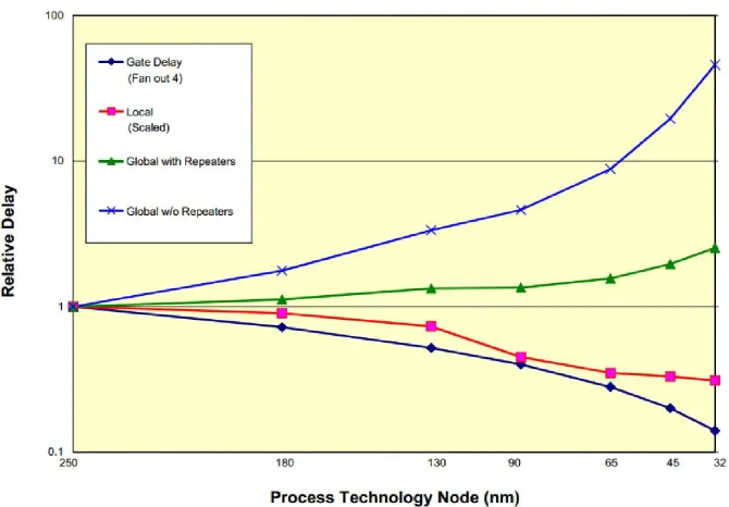
Fig. 3. Delay for metal-1 and global wiring versus feature size. From 180nm to 15nm, the delay of scaled wires increases by approximately 10ps while that of fixed length wires increases by approximately 2000ps. If these wires are modified with repeaters, the delays substantially reduces to roughly single digit (~ 3ps) for scaled wires and 40ps for fixed length wires [2.12].
is 50mils in length, it will have an inductance of 1.3nH. The interconnects interface primarily to the die is required to provide a low impedance path for the power distribution system so as to keep the switching noise within specification and controlled impedance for the signal leads to allow adequate signal integrity. Pak et al. conducted a study where wire-bonding was applied to a multi-stack chip design. Similarly, work was performed for a multi-
Fig. 4. Side-by-side comparison of wire-bond technology versus TSV technology [2.15].
due to lower lead inductance. The typically short length of the FC bonding means less power and ground inductance. Other advantages include higher pad count for power and ground pads and the potential to decrease the impedance of the power and ground distribution network. The primary motivation behind FC is the large input/ output (I/O) count which increases the signal bandwidth for a small die size area. Flip-chip technology utilizes solder bumps to carry large amounts of current for high speed clock applications. The solder bumps introduce negligible parasitic inductance and capacitance at its connections compared to conventional wire-bond connections [2.16]. The advantages of the solder bump interconnection technology over wire bonding technique are listed below [2.16]:
Carry large currents with negligible parasitic inductance and capacitance and low resistance due to short solder bumps.
Capable of achieving better reliability by reducing thermal stress by optimizing solder joint geometry, using underfilling and compliant substrate.
Easy integration to multilayered structures Robust packaging
Table 2.1 summarizes the parasitic properties of solder bump and wire-bond interconnects. The values show a considerable decrease in parasitic values in solder bumps. The solder bumps are mounted face to face onto the interconnect substrate. This is usually viewed as flipped orientation, hence the name, flip chip.
Table 2.1 Summary of Electrical Properties for Wire Bond vs. Solder Bump mΩ/ inch nH/ inch Length Resistance Inductance
Wire Bond 1 25 50-100 mils 50-100 mΩ 1.2 - 2.5 nH
The performance at high frequency applications makes solder bump a superior interconnect compared to the other forms of wire-bond because the connection path length is reduced. Although solder bump offers great benefit over other interconnects, there are disadvantages: These disadvantages are listed as follows: 1) difficult testing of bare dies, 2) limited availability of bumped chips, 3) low reliability for some substrates, 4) high assembly accuracy is required and 5) weak process compatibility with SMT. The evolution of the next generation interconnect technology is TSV for complex 2.5D and 3-D system integration design. TSVs have an advantage compared to other interconnect bonding approaches shown in Table 2.2. The academic research community and semiconductor industry are pushing for TSV interconnect as the choice for 3D integration applications.
Table 2.2 Comparison of TSVs and current interconnect options [2.17].
Technology Advantages Disadvantages
Wire-bonding
Flexible Connections High reliability Mature processing Cost effective
Low density Long thin wire Large pad area Poor signal integrity Poor power integrity
Solder Bumps (FC)
Short Length Low resistance More Connections
Large solder balls May short circuit with
each other in the long run
Through Silicon vias
(TSVs)
Small height Small footprint High density Low resistance
Complex fabrication Capacitive coupling to
substrate, devices and TSVs in vicinity Mechanical stresses to
thin substrate and devices
Contactless i.e. inductive or capacitive coupling
Small electric path length Easy to fabricate
Low reliability
Cross talk and coupling issues
Fig. 5. BEOL Technology requirement for Logic (MPU/ASIC) and NAND flash memory [1.9]
Three-dimensional integration using TSV is one of the future IC packaging technologies that can eliminate copper wire between silicon chips by vertically stacking chips on top of each other. Through silicon vias with heights comparable to the substrate thickness, can pass through the substrate and can be placed anywhere in the chip thus offering additional I/O flexibility compared to copper wires which can only be placed along the peripheral area [2.18].
2.2 Background of TSV Technology
Through silicon via allow interconnection of multiple chips in a vertical direction. The fabrication process and design of TSVs vary significantly and are dependent on the target application. Fig. (6): illustrate a drawing of three different TSV structures consisting of substrate, electrical conductor and dielectric insulator to separate conductor from substrate.
Fig. 6. Cross-section view of TSV designs. A) solid metal filled TSV, b) annular metal-lined TSV and c) TSV with tapered side wall [2.20].
The physical geometries of the TSV are important because they all influence the TSV’s electrical characteristics (e.g. resistance, inductance, capacitance and conductance). The metal filling typically used in TSVs is Cu with a dielectric material of silicon dioxide (SiO2)
or silicon nitride (Si3N4) to isolate the copper cylinder from the substrate material. The
important physical parameters of a TSV are the TSV’s height, diameter, aspect ratio, oxide layer thickness and pitch between other TSV structures.
cross-sectional area. The cross-cross-sectional area of the TSV is inversely proportional to its resistance. To keep the resistance of the TSV minimum will require keeping the cross-section area low. TSVs can be formed at different stages of the fabrication process. TSVs can be formed before BEOL metallization is performed (via-first), between different BEOL metallization steps (via-middle) or after all BEOL metallization is complete (via-last). The detail of each via process step is explained in the following manner: In a via-first process, the vias connect to the local interconnect layer of the BEOL which is used for local routing. In a via-middle process, the vias connect to a higher interconnect layer but uses less local routing a little more global routing. In a via-last process, the vias connect to the highest metal layer which is the global interconnect layer. The global interconnect layer connects to the redistribution layer (RDL) which is at the top of the regular interconnect layers.
2.3 TSV Benefits
With SoC technology developed to miniaturize two-dimensional IC design and boost functionality a little more, the performance, form-factor, scalability and power reduction specifications are becoming increasingly difficult to meet. TSV technology is a conceptual leap from SoC designs and a realization in some technology areas like DRAM memory. In the next few sections, the costs benefits of applying TSV technology over conventional approaches are listed as follows:
2.3.1 Performance:
that memory performance benefits of up to 25% could be realized [2.21]. These improvements are realizable with TSV technology and chip stacking methodologies.
2.3.2 Form-factor:
Over several decades, shrinking transistor size has shown to be very successful method for cramming more switching devices onto a single chip. However, the laws of physics prevent continued shrinkage of switching devices. Some key advantages of small form factor systems include portability, low power consumption, increase functionality and increase I/O bandwidth. Furthermore, Davis et al. reported a 3x reduction in total silicon area and a 12x reduction in chip footprint for a monolithic 3D-IC with 4 device layers when compared to a 2D-IC [2.24]. A quantitative comparison of 3D-IC and 2D-IC design and performance is shown in Table 2.3 to demonstrate the benefits of 3D-IC form factor.
Table 2.3 Monolithic 3D-IC versus 2D-IC using similar technology node [2.25].
22 nm mode 2D-IC 3D-IC
Frequency 600 MHz 600 MHz
Metal Levels 10 10
Average Wire Length 6µm 3.1µm
Av. Gate Size 6 W/L 3 W/L
Die Size (active silicon area) 50mm² 24mm²
Power
Logic = 0.21W
Reps. = 0.17W
Wires = 0.87W
Clock = 0.33W
Total = 1.6W
Logic = 0.1W
Reps. = 0.04W
Wires = 0.44W
Clock = 0.19W
Fig. 7. Interconnect total dynamic power breakdown [2.26]
2.3.3 Scalability:
Interconnect scaling using TSVs enable wire interconnects the capability to keep up with technology node scaling. TSVs can be reduced down in geometry (e.g. height and radius) whereas wire-bond technology struggles. Table 2.3 show the area and power benefits.
2.3.4 Interconnect Power Reduction:
Interconnect power studies and analysis shows that interconnection accounts for over 50% of the dynamic power consumption in high-performance microprocessor [2.22], [2.23]. As a first order approximation, the interconnections are divided into two categories based on the design hierarchy (local and global interconnects). The local and global interconnects show different capacitance characteristics as a function of length. The local interconnects have approximately 25% of interconnect capacitance while the global interconnect capacitance component have about 80%. Although global interconnect capacitance is larger, the interconnect-power peak for the local interconnect nets is higher and it dissipates more dynamic power than global interconnect nets. This is mainly due to the local clock and signal nets. With 3-D integration using TSV technology, TSV parasitics such as capacitance
37%
29% 21%
13%
♦ Global Signals [21%]
♦ Global Clock [13%]
♦ Local Signals [37%]
and resistance by controlling the physical dimensions of the TSV. This is investigated further in chapter 3.
2.4 Electrical Modeling of TSVs
A myriad number of research literatures on packaging technology and interconnect structures that affects power and signal integrity has been published in the last two decades [2.26]-[2.69]. Today several semiconductor companies and national laboratories are investigating approaches to enhance their fabrication process of TSV-based technology for developing stacked systems. Although TSV technology is a critical interconnect component in the development of 3-D integration and replacement of wire-bond technology, accurate electrical characterization of TSV is essential and needed to address power delivery and signal integrity challenges in the future.
The fabrication of TSV process vary due to a number of factors that includes type of metal used to fill TSV, the silicon height, aspect ratio of the TSV, TSV shape and other physical design parameters. Moreover, there are different TSV methods that can be implemented during the IC fabrication process: (1) via-first, (2) via-middle and (3) via-last. The most common TSV shape is cylindrical. However, TSVs can be fabricated in either cylindrical or in a square shape. Once the shape is formed, a barrier is formed to prevent metal from diffusing into the silicon substrate. Tantalum (Ta), Titanium Nitride (TiN) or the most often used silicon dioxide (SiO2) is used as barrier materials. Copper-based metals are
used to fill the TSVs because they have lower resistivity than aluminum (Al), Tungsten (W) and Polysilicon material [2.57], [2.65].
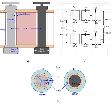
RTSV/2 LTSV
COX
GOX
CDEP
GDEP
CSi
GSi RTSV/2
COX
GOX
CDEP
GDEP
CSi
GSi
RTSV/2
LTSV
RTSV/2 arranged in different signal-power configurations e.g. P/G, GSG, GSSG, GPPG (G-ground, P-power and S-signal) [2.29]-[2.36],[2.48]-[2.53] and [2.55]-[2.64]. These papers do not require using large matrix solution techniques but they study the properties of basic TSV configurations and their parasitic characteristics (RLGC). Finally, there are published works
Fig. 8. (a) Power and ground TSV pair including, (b) equvalent circuit parasitic model and (c) top view with radius outlined.
(a)
(c)
that study the impedance properties of TSV-based power delivery networks and interconnect structures affecting the on-chip signal integrity [2.60], [2.62],[2.65]-[2.70]. Fig. (8): shows a power-ground TSV pair and equivalent circuit parastic model used to characterize the impedance property of the TSV. The equivalent circuit parasitic model includes parasitic resistance, inductance, capacitance and conductance. Each parasitic is described below including a general closed form expression considering the TSV diameter, TSV length, TSV dielectric liner thickness, TSV pitch and silicon conductivity. The closed form expression offers a fast and accurate method to calculate the TSV impedance of the network.
(i) Resistance:
The TSV resistance is a function of the length of the TSV, cross-sectional area of the TSV and the conductivity of the silicon material. The parameters affecting the resistance of the TSV are surface scattering, boundary scattering and the skin effect. There are two types of resistance: (1) the static resistance or DC resistance of the TSV and (2) high-frequency resistance of the TSV [2.30].
=
(2.1a)
=
( )
(2.1b)
=
+
(2.1c)
and reduces exponentially with distance. The skin effect which reduces the effective cross-sectional area of TSV lowers the TSV resistance. Eqn. (2.1b) describes this behavior.
(ii)Inductance:
The TSV inductance is determined by the TSV length, TSV diameter and current return path. The inductance is primarily based on the loop formed as current travels into and out of the TSV. The inductance in an integrated circuit is very difficult to determine because of multiple current return paths (tens or even hundreds of returns paths). There are a few effects at high-frequency that changes the current distribution inside a TSV. The first effect is the skin effect and the other effect is the proximity effect. When current flows in the same or opposite direction, the proximity effect reduces the overall inductance in a TSV. Moreover, there is another high-frequency effect that changes the inductance of a TSV and that is the multiple current in the return paths. When the current is redistributed among the many return paths, the overall impedance of the path is minimized. Conclusively, given the frequency, certain return paths will minimize the total impedance than other return paths.
The loop inductance is characterized by two components: (1) self-inductance and (2) mutual inductance. An expression for the self-inductance is [2.30], [2.35] and [2.52]:
= + − + +
(2.2a)
= + − +
(2.2b)
To calculate the total loop inductance, one must combine the self and mutual inductance expressions of Eqns. (2.2a) and (2.2b). The total loop inductance is:
=
+
− 2
(2.2c)
(iii) Capacitance
Similar to the previously mentioned components, the TSV capacitance is characterized by the material properties and physical dimensions of TSV. However, there is another important effect beyond the physical characteristics and material properties that affects the capacitance. This is the effect of the electric field lines and how they terminate to nearby metals and TSVs. The field lines radiate from the TSV conductor and terminate to a back metal reference (ground) plane. A depletion region is formed around the TSV and is considered into the closed-form expressions published in several
The analytical expressions used for electrically characterizing the different capacitor models of a TSV are shown in Eqn. (2.3). The closed-form capacitor model for Cox describes a capacitance that is isolated from the conductive silicon and represents half of the whole oxide capacitance.
where the TSV physical design and material parameters are TSV length, , TSV diameter, , the pitch between TSV pair, , and the silicon dioxide thickness,
. The depletion region capacitance is characterized by:
=
(2.3b)
where is the maximum depletion radius, is the radius from the center of TSV conductor to the oxide layer and is the radius of the TSV.
=
∙
(2.3c)The total capacitance of the TSV structure is expressed using the following closed-form expression:
=
∙+
(2.3d)In later works, more closed-form expressions of the TSV capacitance were developed based on TSV bundling where self and inter-via coupling capacitance between each and every TSV are defined.
(iv) Conductance
conductance of the silicon substrate is primarily based on the amount of majority carrier concentration. The closed-form expression of the silicon substrate conductance is represented in Eqn. (2.4a):
=
(2.4a)
where , is the conductivity of the silicon substrate and is silicon permittivity. The oxide conductance is characterized using the following expression:
=
(2.4b)
The depletion conductance expression used considers the threshold voltage, , the applied voltage, and the depletion region width, .
=
∙
∙ 2
(2.4c)
The total TSV conductance is estimated using the following expression.
=
+
(2.4d)
Chapter Summary
CHAPTER III
Parametric Modeling of On-Chip
Interconnects
3.1 Back-End of Line (BEOL) for Power Grid Structures
Back-end of line (BEOL) interconnects are used in integrated circuits for the purpose of distributing clocks, high-speed signals and provide power-ground to various logic circuitry across the chip. There are three types of interconnects: local, intermediate and global.
Local interconnects include very thin lines, connecting gates, and transistors within a functional block. They usually span a few gates and occupy the bottom 1st and 2nd layer-levels. The resistance is usually higher at these layers.
Intermediate interconnects are wider and taller than local interconnects. The intermediate interconnects have lower resistance than local interconnects because the widths are wider.
Global interconnects contain clock and signal distribution between functional blocks. Global interconnects deliver power-ground to all functional blocks. The global interconnects reside on the top level of the BEOL layer usually the 1st and 2nd layer
The characteristics of BEOL interconnects at all levels are critical, particularly the local interconnect level. The RC delay of the transistor is determined by the design of the local interconnect layer. Since the resistivity at the local interconnect level is higher than the other interconnect levels (e.g. intermediate and global), the preferred metal material to use in BEOL interconnect process is copper (Cu) instead of aluminum (Al). Copper has a lower resistivity property than aluminum and it’s highly conductive. A lower resistivity interconnect means the RC delay is reduced and the IC speed is increased. The interconnect characteristics for the power grid structure are described in this section. We investigate the variation in power grid dimensions and monitor the parasitic elements (resistance, inductance and capacitance) that directly affect the RC delay and SSN noise (Ldi/dt) behaviors.
In the parametric study, we vary the metal width, metal thickness and metal pitch of the BEOL power grid structure. We begin the parametric study with global interconnect and scale the physical dimensions down to the physical dimensions of at the local interconnect level. The main goal of this analysis is to determine how the metal width, metal pitch and metal thickness affect the inductive, resistive and capacitive characteristics of the BEOL power grid structure. The performance at the IC level is dictated by the electrical characteristics of the BEOL interconnects.
Fig. 9. Interdigitated power/ground pair showing global (top layer) and local (bottom layer) interconnect level [2.19].
Fig. 10.Defined parameters of a unit cell power grid structure used in the parametric study [3.1].
P
0 5 10 15 20 25 30 35 40 0
2 4 6 8 10 12 14
R
e
s
i
s
t
a
n
c
e
[
O
h
m
]
Frequency [GHz] Metal
THK=0.2m
Metal
THK=0.4m
Metal
THK=0.6m
Metal
THK=0.8m
Fig. 11. Parasitic resistance versus frequency for a given metal thickness.
higher dielectric capacitance (Ci per unit area). This results in reduction in operating voltages through reduction in threshold voltage [3.2]. The dielectric thickness was fixed at 0.2-μm. However, the dielectric thickness was varied and increased up to 0.8-μm. The result show the dielectric thickness is inversely proportional to intrinsic capacitance.
0 5 10 15 20 25 30 35 40 2.2 2.25 2.3 2.35 2.4 2.45 2.5 2.55 2.6 2.65 2.7 I n d u c t a n c e [ n H ] Frequency [GHz] Metal
THK=0.2m
Metal
THK=0.4m
Metal
THK=0.6m
Metal
THK=0.8m
thicker metal lines at the local interconnect level means sidewall capacitance increases which raises another signal integrity issue in crosstalk. There is a delicate balance between RC
Fig. 12.Parasitic inductance of unit cell power grid for a given metal thickness.
delay and crosstalk wherein on-chip PDN designers must consider the optimal PDN design and metal routing strategies for local-level interconnects to avoid crosstalk and increase RC delay issues. In this study, we kept the metal thickness fixed at 0.5-μm for the local level.
increased resistance. Techniques to lower the inductance on interconnects should be applied to ground interconnect structures so as to minimize the area of the current loop. As far as the interconnect sidewall capacitance, it can be mitigated by reducing the metal thickness. In summary, reducing the metal thickness lowers parasitic inductance and capacitance. However, the opposite affect is seen with parasitic resistance. In an effort to reduce the RC delay for local-level interconnects, we kept the metal thickness below 0.5-μm to ensure the parasitic capacitance is lowered. This will ensure the overall impedance of the PDN at the local-level is kept low. Conclusively, reducing the metal thickness of the local level interconnect, particularly, the ground interconnect structures will ensure no inductive and capacitive contribution to the PDN.
Fig. 13.Parasitic resistance versus frequency for a given metal width.
In this section, the metal width of the unit cell power grid structure was scaled. Figure (13) show results of the parasitic resistance versus frequency as the metal width varied. The
0 10 20 30 40
0 0.5 1 1.5 2 2.5 3 3.5 4 R e s i s t a n c e [ O h m ] Frequency [GHz] Metal
WDTH=20m
Metal
WDTH=14m
Metal
WDTH=8m
Metal
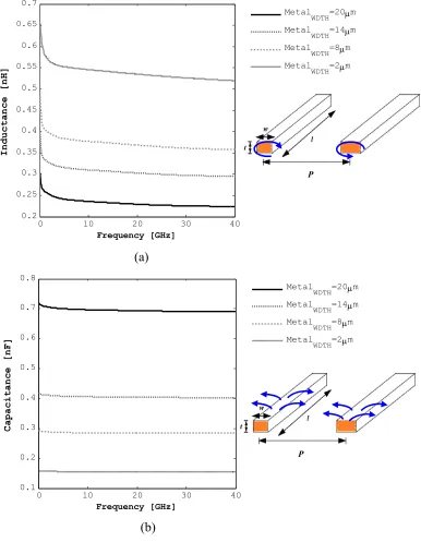
0 10 20 30 40 0.2 0.25 0.3 0.35 0.4 0.45 0.5 0.55 0.6 0.65 0.7 I n d u c t a n c e [ n H ] Frequency [GHz] Metal
WDTH=20m
Metal
WDTH=14m
Metal
WDTH=8m
Metal
WDTH=2m
increase of the metal width has an inverse effect on the parasitic resistance. This is explained when looking at the cross-sectional area of the power grid interconnect. The cross-sectional
Fig. 14.Inductance and capacitance versus frequenncy for a given metal width.
P
0 10 20 30 40
0.1 0.2 0.3 0.4 0.5 0.6 0.7 0.8 C ap a c it a n ce [ nF ] Frequency [GHz] Metal
WDTH=20m
Metal
WDTH=14m
Metal
WDTH=8m
Metal
WDTH=2m
(a)
(b)
area is the product of the thickness times width. The resistance is inversely proportional to the cross-sectional area given the following expression: = ⁄ , where l is the interconnect of the metal line length, ρ is the material resistivity of copper and A is the cross-sectional area of the interconnect denoted by the metal width, w and metal thickness, t. Figure (14) depicts a simulated parasitic inductance and capacitance of a unit cell power grid structure. The metal width is inversely proportional to the parasitic inductance. The behavior of the inductance was observed for a given metal width. As the metal width increased the parasitic inductance decreased. This was not the case for the parasitic capacitance. The width of the power grid interconnect is proportional to the parasitic capacitance. As the metal width increased, the parasitic capacitance increased due to the fringe capacitance. Conclusively, the metal width is another knob that can be used to control the parasitic resistance, inductance and capacitance of the interconnect structure. Also, in figure 14, we show a pair of power ground interconnects where t, represents the interconnect thickness, w is the width and p is the interconnect pitch
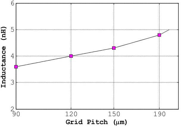
Lastly, the pitch of a unit cell power grid was varied. The pitch or spacing values were obtained from the International Technology Roadmap for Semiconductors (ITRS). We used the following pitch to separate the return and power metal line, 90-μm, 120-μm, 150-μm and 180. Figure 15 shows the parasitic inductance versus metal pitch. In this plot, we observed marginal increase in parasitic inductance of the unit cell power grid structure. The proximity of the power-ground pair constitutes the strength of the inductive and capacitive coupling between the two wires. However, irrespective of the pitch value, the metal pitch has little effect on the parasitic inductance. The dependence of the parasitic inductance relies heavily on the metal line length rather than on the metal pitch [2.19].
width, metal thickness and metal pitch were analyzed for a unit cell power grid using HFSS. The parametric sweep results of the power grid structure support the design of area efficient and robust power distribution grids in high speed integrated circuits. The results of this section are summarized as follows:
The inductance of power distribution grids decreases with increasing signal frequency.
The parasitic resistance of the power distribution grids is controlled using the cross-section area (metal thickness and metal width). The metal width and thickness are inversely proportional to the parasitic resistance.
The parasitic capacitance of the power distribution grid is proportional to the metal thickness and metal width.
The smaller the metal pitch (separation) between the power and ground metal lines and the wider the lines, the more significant the proximity effects become and the greater the relative decrease in inductance with frequency.
Fig. 15.Inductance for a given pitch variation over a wide range of frequencies.
90 120 150 190
2 3 4 5 6
I
n
d
u
c
t
a
n
c
e
(
n
H
)
3.2 Power-Ground TSV Interconnect Pair
In this section, a high-frequency parametric study of a power-ground TSV pair is performed. The power grid model includes a micro-bump and redistribution layer (RDL). The physical dimensions of the RDL and micro-bump have remained constant for the construction of the power deliver network. For the scalability of the power-ground TSV pair, the model is proposed with structural parameters and material properties as indicated in Table 3.1. The analytical RLGC equations of the TSV pair are derived from the physical configuration of the design parameters.
.
Table 3.1
VALUE OF INTERCONNECT COMPONENTS OF A UNIT CELL
Parameter Value
TSV diameter 2x10⁶ m – 30 x106 m TSV height 20x106 m – 110 x106 m
TSV pitch 80x106 m – 200 x106 m TSV Oxide thickness 0.5x10⁶ m - 1x10⁶ m
RDL pad diameter 4x10⁶ m
RDL thickness 1x10⁶ m
PDN grid width 2x10⁶ m - 25x106 m
PDN grid spacing 90x106 m - 200 x106 m
PDN grid thickness 0.2x10⁶ m
PDN grid length 200 x106 m
Substrate conductivity 10-S/m
Micro-bump diameter 20x106 m
Micro-bump height 15.4x10⁶ m
Micro-via height 0.5x10⁶ m
Micro-via diameter 0.25x10⁶ m
RTSV/2
LTSV
COX
GOX
CDEP
GDEP
CSi
GSi
RTSV/2
COX
GOX
CDEP
GDEP
CSi
GSi
RTSV/2
LTSV
RTSV/2
(a)
(b)
R e s i s t a n c e [ O h m ] Frequency [GHz] d
tsv=5m
d
tsv=10m
d
tsv=20m
d
tsv=30m
0 10 20
0 0.05 0.1 0.15 0.2 R e s i s t a n c e [ O h m ] Frequency [GHz]
R
e
s
i
s
t
a
n
c
e
[
O
h
m
]
Frequency [GHz] htsv=40m
h
tsv=60m
h
tsv=80m
h
tsv=110m
0 10 20
0 0.05 0.1 0.15 0.2 0.25 0.3
R
e
s
i
s
t
a
n
c
e
[
O
h
m
]
Frequency [GHz]The table above shows the physical design parameters used to construct a unit cell power grid structure. The values for the TSV height, diameter, pitch and oxide thickness used during the parametric study will denote the parasitic resistance, inductance and capacitance characteristics. The results of the parametric study are used to design TSV-based power grid.
(a)
(b)
R e s i s t a n c e [ O h m ] Frequency [GHz]
=20 Ohm-cm
=10 Ohm-cm
=5 Ohm-cm
=3 Ohm-cm
=2 Ohm-cm
0 10 20
0 0.02 0.04 0.06 0.08 0.1 R e s i s t a n c e [ O h m ] Frequency [GHz] R e s i s t a n c e [ O h m ] Frequency [GHz] p
tsv=80m
p
tsv=120m
p
tsv=160m
p
tsv=200m
0 10 20
0 0.05 0.1 0.15 0.2 0.25 0.3 R e s i s t a n c e [ O h m ] Frequency [GHz] (a) (b)
Fig. 18.Variation of TSV resistance with its (a) pitch and (b) resistivity.
R e s i s t a n c e [ O h m ] Frequency [GHz] t
ox=0.5m
t
ox=0.7m
t
ox=1m
0 10 20
0 0.02 0.04 0.06 0.08 0.1 R e s i s t a n c e [ O h m ] Frequency [GHz]
Fig. 19.Variation of TSV resistance with oxide thickness.
pitch and oxide thickness) as a function of frequency. For each physical design parameter, the values were swept using 3D field solver, HFSS of Ansoft. Figure 17(a) shows a plot of the TSV resistance for a given TSV diameter, . By increasing the TSV diameter, the resistance of the P/G TSV is decreased. The TSV diameter ranged from 5-μm to 30-μm. The other design parameters were constant during the sweep.
pitch without exceeding the maximum resistance allowed for a given design application.where WA is the wafer-to-wafer alignment overlay and is the minimum metal-to-metal spacing, R is the TSV resistance, is the taper angle of the TSV cavity, is the oxide thickness of the TSV and ℎ is the TSV height.
Figure 18(b) is a plot of the TSV resistance for a given silicon resistivity, (or conductivity, = 1⁄ ). The silicon resistivity is a material property that is capable of having significant effect on the electrical characteristics of the P/G TSV. The resistive loss from a TSV is through the silicon substrate. The parameters and determine the overall insertion loss of the P/G TSV channel. As the silicon resistivity increases from 2 Ohm-cm to 20 Ohm-cm the conductance ( and ) of the silicon substrate decreases. As a result, the overall insertion loss of the P/G TSV channel decreases. In conclusion, the physical design parameters for the P/G TSV aren’t the only physical parameters that affect TSVs but the material property of the silicon substrate has an impact on the electrical characteristics of the TSV.
The TSV resistance for a given oxide thickness is plotted in Figure 19. The variation in oxide layer thickness goes from 0.5-μm to 1-μm. The oxide layer thickness protects the TSV from the influence of the conductivity of the silicon substrate layer. The TSV resistance is marginally affected by the oxide layer thickness since the radius between the TSV metal copper area, and is marginal. To observe a considerable increase in TSV resistance, the TSV radius, , value has to be large.
C a p a c i t a n c e [ f F ] Frequency [GHz] d
tsv=5m
d
tsv=10m
d
tsv=20m
d
tsv=30m
0 10 20
0 10 20 30 40 50 C a p a c i t a n c e [ f F ] Frequency [GHz] C a p a c i t a n c e [ f F ] Frequency [GHz] h
tsv=40m
h
tsv=60m
h
tsv=80m
h
tsv=110m
0 10 20
0 20 40 60 80 C a p a c i t a n c e [ f F ] Frequency [GHz] C a p a c i t a n c e [ f F ] Frequency [GHz] p
tsv=40m
p
tsv=80m
p
tsv=120m
p
tsv=160m
0 10 20
0 5 10 15 C a p a c i t a n c e [ f F ] Frequency [GHz] C a p a c i t a n c e [ f F ] Frequency [GHz]
=20 Ohm-cm
=10 Ohm-cm
=5 Ohm-cm
=3 Ohm-cm
=2 Ohm-cm
0 10 20
0 5 10 15 C a p a c i t a n c e [ f F ] Frequency [GHz] C a p a c i t a n c e [ f F ] Frequency [GHz] t
ox=0.3m
t
ox=0.5m
t
ox=0.7m
t
ox=1m
0 10 20
0 5 10 15 20 25 30 C a p a c i t a n c e [ f F ] Frequency [GHz]
Fig. 21.TSV Capacitance parametric sweep of design parameters (a) , (b) , (c) , (d) and (e) .
(a) (b)
(c) (d)
Figure 21 shows the simulated TSV capacitance between two TSVs as a function of the diameter, height, pitch, silicon resistivity and oxide layer thickness. The TSV capacitance consist of two components: (1) the oxide layer capacitance formed between the TSV copper and the silicon substrate layer, and (2) the capacitance formed between two TSV structures where the silicon substrate separated the P/G TSVs, . The TSV capacitance is the total parasitic capacitance of the P/G TSV pair.
The diameter of the TSV is swept from 5-μm to 30-μm. Figure 21 shows the TSV diameter is a function of the TSV capacitive property and is directly proportional to each other. As the diameter increases, so does the overall TSV capacitance as the TSV pitch and height between P/G TSV pair remains fixed. By increasing TSV diameter, in effect, and parameters are increased. At low frequency the overall TSV capacitance is high but drops significantly as the frequency increases.
The height of the TSV is simulated from 40-μm to 110-μm. The TSV height takes on a similar behavior as the TSV diameter. As the TSV height increases, the capacitive property of the TSV increases. The TSV height has the largest impact on the capacitive property relative to , , or . The spacing between P/G TSV has an effect on the TSV capacitance. The strength of the electric field is dictated by the TSV pitch. As the TSV pitch increases, the TSV capacitance reduces. This is more apparent at frequencies between 2 GHz and 7 GHz. At frequencies above 10 GHz, the TSV capacitance converges to a single value of 3 GHz.
I n d u c t a n c e [ p H ] Frequency [GHz] d
tsv=5m
d
tsv=10m
d
tsv=20m
d
tsv=30m
0 10 20
5 10 15 20 25 30 35 40 I n d u c t a n c e [ p H ] Frequency [GHz] I n d u c t a n c e [ p H ] Frequency [GHz] h
tsv=40m
h
tsv=60m
h
tsv=80m
h
tsv=110m
0 10 20
20 40 60 80 100 120 I n d u c t a n c e [ p H ] Frequency [GHz] I n d u c t a n c e [ p H ] Frequency [GHz] p
tsv=80m
p
tsv=120m
p
tsv=160m
p
tsv=200m
0 10 20
10 20 30 40 50 60 70 80 I n d u c t a n c e [ p H ] Frequency [GHz] I n d u c t a n c e [ p H ] Frequency [GHz]
=20 Ohm-cm
=10 Ohm-cm
=5 Ohm-cm
=3 Ohm-cm
=2 Ohm-cm
0 10 20
18 19 20 21 22 23 24 I n d u c t a n c e [ p H ] Frequency [GHz] I n d u c t a n c e [ p H ] Frequency [GHz] t
ox=0.5m
t
ox=0.7m
t
ox=1m
0 10 20
18 19 20 21 22 I n d u c t a n c e [ p H ] Frequency [GHz]
Fig. 22.TSV Inductance parametric sweep of design parameters (a) , (b) , (c) , (d) and (e) .
(a) (b)
(c) (d)
The inductive property of the P/G TSV with variation in height, diameter, pitch and material property is described in Figure 22. We use the same physical design parameters used during the analyses of the TSV resistance, , and TSV capacitance, , to analyze the behavior of the TSV inductance. The inductance for a single TSV structure is mainly determined by the TSV height, diameter and material property. For a P/G TSV pair, the TSV pitch becomes an important parameter because of the formation of the inductive loop (coupling inductance and self-inductance) given the spacing of the return path.
The TSV conductance is another electrical component capable of changing the electrical characteristics of the TSV. The conductance of the TSV is composed of two distinct parameters which are: (1) the silicon dioxide conductance, and (2) the silicon substrate conductance, . The TSV conductance has been simulated and plots have been generated. The simulated plots of the TSV conductance can be found in Appendix A. In summary, we present in Table 3.2 of the parasitic circuit element (RLGC) with respect to the variation in physical design parameters based on a P/G TSV model. The table shows how TSV resistance, inductance, capacitance and conductance respond when physical size of the TSV and material property of the silicon substrate change.
Table3.2
TSV Design Parameter Impact on RLGC elements ℎ
Note: Increase and decrease of design parameters are denoted by direction of arrow.
![Fig. 1. A trend of on-chip interconnect [1.2].](https://thumb-us.123doks.com/thumbv2/123dok_us/1330580.1166013/16.612.195.446.129.349/fig-trend-chip-interconnect.webp)
![Table 1.1 Intel Microprocessor Trends of last decade [1.8].](https://thumb-us.123doks.com/thumbv2/123dok_us/1330580.1166013/18.612.99.534.302.619/table-intel-microprocessor-trends-decade.webp)
![Fig. 2. Electromagnetic view of a wire [2.13]. If the current (I) and voltage (V) change at the drive point, the magnetic (B) and electric (E) change as well; disturbance propagates away from the drive point at the speed of light](https://thumb-us.123doks.com/thumbv2/123dok_us/1330580.1166013/26.612.226.409.192.515/electromagnetic-current-voltage-change-magnetic-electric-disturbance-propagates.webp)
![Fig. 4. Side-by-side comparison of wire-bond technology versus TSV technology [2.15].](https://thumb-us.123doks.com/thumbv2/123dok_us/1330580.1166013/28.612.143.486.271.481/fig-comparison-wire-bond-technology-versus-tsv-technology.webp)
![Table 2.3 Monolithic 3D-IC versus 2D-IC using similar technology node [2.25].](https://thumb-us.123doks.com/thumbv2/123dok_us/1330580.1166013/35.612.110.520.441.674/table-monolithic-ic-versus-using-similar-technology-node.webp)