OPTICAL COUPLING FOR MULTI-LAYER PRINTED WIRING BOARD BY
SELF-WRITTEN WAVEGUIDE
Nurul Atiqah Baharudin
1, Sumiaty Ambran
1*, Osamu Mikami
1**, Chiemi Fujikawa
2 1Malaysia Japan International Institute of Technology, Universiti Teknologi Malaysia, Malaysia
Email: [email protected]
Email*: [email protected]
Email**: [email protected]
2Tokai University, Japan
Email: [email protected]
ABSTRACT
For the future of optical interconnect, high optical coupling efficiency is required for high density multilayer optical printed wiring board (OPWB). Hence, we propose optical pin as optical coupling devices between surface devices and the multi-layer channel of OPWB using self-written waveguide (SWW) with mask-transfer method. SWW-pin is passively aligned and mask-transfer provides precise positioning between surface device and channel waveguide. This makes these technology is a promising technology for coupling device. A comparison of coupling efficiency of three cases methods is performed-using ray-tracing simulation. The calculation for optical coupling efficiency with vertical pin of -0.05 dB is achieved. The proposed of an easy and sufficient fabrication concept using MTSW method with the application of prism are expected. The vertical pin technologies are anticipated to be useful in the future of high optical coupling devices of the multi-layer and multi-channel waveguides and /or a multi-core optical fiber.
Keywords— Optical coupling device, ray tracing simulation, self-written waveguide (SWW), Mask-Transfer Self (MTSW), optical pin, multi-layer printed wiring board
1. INTRODUCTION
With the dramatically enormous rapid growth in recent information technology (IT) development, a remarkable explosion in the information flow in the network necessitates more excellent network capacity and speedy signal processing in IT equipment and hardwares. Back then, metallic wiring was widely used for data transmission; however, restraint in a number of problems includes signal degradation, bandwidth, impedance matching, crosstalk between adjacent channels, large power utilization, electromagnetic interference (EMI), bulky mass and huge footprints have become acute bottlenecks in conventional electric wiring, even inside of a box [1]. To address these issues, optical interconnect technology as expected to solve these problems has become the focus of active researches and development in board-to-board and chip-to-chip interconnection. The introduction of “linking with optics” in replacement of "metallic wirings" is just a short cut [2], due to the limitations of optical wiring in the context of optical
connections such as high optical coupling efficiency needs excessively fine alignment have become the issues. To overcome this issues, a sophisticated packaging and coupling technologies yet cost-effective are needed to develop practical optical interconnection that enables both large coupling efficiency and easy alignment for high speed optical printed wiring board (OPWB).
Currently, most waveguide devices are channel on one substrate plane by mean waveguide formed only on one plane. In spite of that, the structure of OPWB has been expand ahead from a single optical layer to multiple optical layers [3]. Since OPWB is going to be multi-channeled and multi-layered [4], waveguides (1 x N channels) will be a leading for the future of optical interconnect with high density and large capacity.
High speed, high density, and small power consumption multi-layer OPWB is required for the next generation of high performance routers and servers. However, due to increasing inter channel crosstalk and propagation loss at high speeds such as more than 10 Gbit/s/channel, at data transmission become resistance.
For high speed and huge capacity interconnection, Shishikura et al [3] successfully demonstrated 10-Gbit/s/channel operation and developed a multi-layer OPWB using a cube-core structure as an optical confinement that react as a waveguide core or a lens that is simultaneously occur in the waveguide core fabrication methods. Hence, high optical coupling efficiency between optical devices and the lower waveguide layer for high-density optical interconnections can be achieved.
Thus, we interested in the optical coupling for surface device (such as Vertical-cavity surface-emitting laser (VCSEL) or photodiode (PD)) and multi-layer channels using self-written waveguide (SWW) with mask-transfer method.
2. PROPOSED DEVICE CONFIGURATION
Transmitting signal from surface devices (VCSEL/PD) to multi-layer channel mounted on an OPWB needs both high optical coupling efficiency and easy alignment device. Given these circumstances, we propose optical coupling device with vertical optical coupling pillar called “optical pin” patterned by (SWW) with mask-transfer method. The cross sectional view of our proposed optical coupling device structure is shown in Figure 1. These optical pins coved with cladding resin can passively grow using SWW and precisely aligned at the end of channel with the mask-transfer methods. The SWWs and the circular windows of the photomask aperture and optical waveguide channels of the OPWB were precisely aligned under an optical microscope.
Previously, this device is applied to hybrid-integrated Si-photonics-based optical I/O cores, which is developed by Japan National Research Project Team (PETRA) and has been presented at OFC (Optical Fiber Conference, March 2015) [7][8]. The proposed device has a great additional advantage and interesting structure. By adding in prism, built-in alignment scheme become sufficient. Improved of optical coupling efficiency is expected to be achieved when the optical pin coupling device is coupled between surface devices (VCSEL/ PD) and the multi-layer channel of OPWB due to the accurately targeted by mask-transfer method. This concept has the advantage of providing high density multi-layer OPWB.
Figure 1 Cross sectional view of proposed optical coupling device structure (Case 1).
3. COMPARISON OF COUPLING METHODS
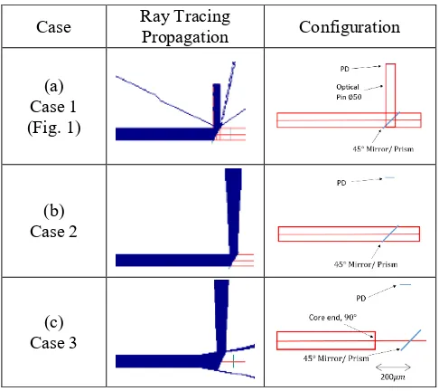
For the future of optical interconnect with high density and large capacity OPWB, configuration of multi-layers and multi-channels is necessary. However, the obstacle of optical coupling scheme between surface devices (VCSEL/ PD) and the multilayer channel of OPWB become our priority and concern, not the coupling between channels at the end face and optical devices/ fibers. Therefore, three configuration structure were considered and discussed as below;
i. Case 1: vertical pin coupling between surface devices (VCSEL/ PD) and the multi-layer channel of OPWB (refer Fig.1)
ii. Case 2: no vertical pin, core end at 450
iii. Case 3: no vertical pin, core end 900
Configuration of multiple channel and multiple waveguide for (a) No vertical pin, core end, 450 and (b) No vertical pin,
core end, 900, 𝑔𝑎𝑝 200 𝜇𝑚 shown in Figure 2.
(a) Case 2
(b) Case 3
Figure 2 Configuration of multiple channel and multiple waveguide for (a) No vertical pin, core end, 450 and (b) No
vertical pin, core end, 900
Case Ray Tracing Propagation Configuration
(a) Case 1 (Fig. 1)
(b) Case 2
(c) Case 3
Figure 3 Schematic diagram of beam propagation and Ray configuration of Ray Tracing Method for (a) With vertical pin, (b) No vertical pin, core end, 450 and (c) No vertical
pin, core end, 900, gap 200 𝜇𝑚
A comparative study was simulated with ray tracing software OptiCAD® (OptiCAD Corp.). Schematic diagram of beam propagation and Ray configuration of Ray Tracing Method for (a) With vertical pin, (b) No vertical pin, core end, 450
in Figure 3. These three configurations is assembled with photodiode (PD) and film in core.
Base on Case 1, few losses shown in beam propagation due to reflection and refraction. However, it narrowed and focusing due to the optical pin for the ray configuration. Next, for Case 2, broader reflection shown for beam propagation and ray configuration. Finally for Case 3, beam propagation shows some refracted pass through the mirror and reflected farther from PD for the ray configuration.
Table 1. Coupling efficient of the OWP by OPTI-CAD simulation.
Case
Ray reaching film in core (total 1089)
Ray reaching
PD
Coupling efficiency,
𝜂 (dB)
Case 1 1089 1077 −0.05
Case 2 1089 799 −1.34
Case 3 1089 489 −3.48
The coupling efficiency of the Optical Waveguide Plugs (OWPs) of the optical connection rods is summarized in Table 1. The equation for coupling efficiency will be given by;
𝜂 (𝑑𝐵) = 10 log10
Ray reaching PD Ray reaching film in core
The ratio between the numbers of rays reaching PD with the number of rays reaching film in core is calculated for the coupling efficiency.
For each cases, 1089 ray is reaching the film in core without loss. From the results, we realized that ray reaching PD is various for 1077, 799 and 489 respectively for each cases. This mean greater beam diverge for Case 3 followed by Case 2 than Case 1 through travelling to reach PD. Crosstalk occur due to the ray loss.
As a result, the coupling efficiency is maximum for Case 1 (-0.05 dB) which is greater than Case 2 (-1.34 dB) and Case 3 (-3.48 dB). We conclude that the coupling efficiency for Case 1 > Case 2 > Case 3 and descending Case 1 < Case 2 < Case 3 for crosstalk. Without vertical pin, beam flux become diverge and high density channel becomes difficult. This showed that vertical pin maximizing the coupling efficiency and minimizing the crosstalk between channels.
4. MASK-TRANSFER SELF-WRITTEN WAVEGUIDE TECHNOLOGY
The self-written waveguide (SWW) technology with light-curable resin is one of the potential technologies to achieve practical packaging and coupling technologies to enable both high coupling efficiency and simple alignment [9][10][11]. SWW technique has advantageous in 1) great mechanical strength, 2) less alteration of optical coupling loss, and 3) unnecessary alignment in between an optical wiring and an SWW [2][12]. Furthermore, under UV light irradiation, the SWW method that allows fabrication of an optical channel waveguide, grows from the end face of the optical fiber, the growth is homologous to that of an icicle [13]. Extremely
large coupling efficiency between the fiber and fabricated waveguide core can be achieved [4]. A previous study in SWW has been introduced for realization of optical interconnection [14]. Moreover, using this so called “optical soldering” technology is a great promising to reduce the alignment difficulties. It is also suitable to perform the various shape OWPs on the optical devices [15].
The extended Mask-Transfer Self-Written (MTSW) to improve the contact exposure of the UV-curable resin by a current photomask and developed from the "classic" fiber-SWW technology which only can produce a single 1-channel waveguide at a time. A UV-curable resin (SUNCONNECTTM, Nissan Chemical Industries, Ltd.) is injected into a gap between the substrate and photomask; the thickness of the fabricated device is controlled by the gap size. At room temperature, the SWWs were grown. When the UV light is irradiated, the photomask aperture is precisely controlled the photomask and the cross section of SWWs [4]. MTSW technique is advantageous whereas it can be assembled at single shot of UV light and by using M x N arrayed photomask patterns it can be efficiently extended to matrix-arrayed optical interconnection of multi-optical layers and multi-optical waveguide channels [16]. Figure 4 shows schematically the MTSW method. By using MTSW technologies, several new optical interconnect device have been proposed and fabricated [17].
Figure 4 The concept of MTSW method of fabrication process [14].
Figure 5 Fabrication samples of 4 x 4 arrayed optical connection rods [14]. (a) samples of square aperture
patterns, (b) samples of round aperture patterns
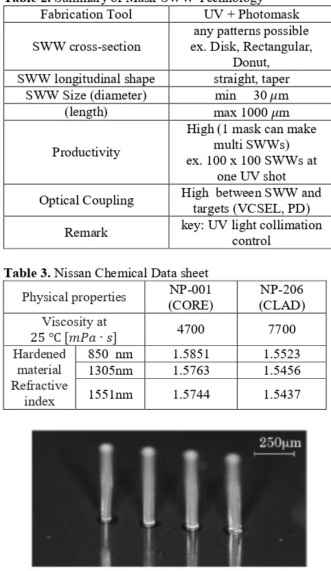
Fabrication samples of 4 x 4 arrayed optical connection rods shown in Figure 5, (a) samples of square aperture patterns, (b) samples of round aperture patterns, with period of 100𝜇𝑚
refractive index of the representative grade is shown in Table 3 is used for the set up. Figure 6 shows fabrication of OWPs with 250𝜇𝑚 pitches [18].
Table 2. Summary of Mask-SWW Technology Fabrication Tool UV + Photomask
SWW cross-section ex. Disk, Rectangular, any patterns possible Donut, SWW longitudinal shape straight, taper
SWW Size (diameter) min 30 𝜇m
(length) max 1000 𝜇m
Productivity
High (1 mask can make multi SWWs) ex. 100 x 100 SWWs at
one UV shot Optical Coupling High between SWW and targets (VCSEL, PD)
Remark key: UV light collimation control
Table 3. Nissan Chemical Data sheet
Physical properties (CORE) NP-001 (CLAD) NP-206 Viscosity at
25 ℃ [𝑚𝑃𝑎 ∙ 𝑠] 4700 7700 Hardened
material Refractive
index
850 nm 1.5851 1.5523
1305nm 1.5763 1.5456
1551nm 1.5744 1.5437
Figure 6 Fabrication of OWPs [18].
4. FABRICATION METHOD
Figure 7 shows a schematic concept of the proposed optical coupling device. Figure 7 (a) is a concept image. Figure 7 (b) is an overall fabrication process. The fabrication process is summarized as follows;
i. Place a prism with an angle of 45° on the bottom of multi-layered optical wiring board, inject space with light-curable core resin.
ii. Cover with an alternate white and black stripes photomask, irradiate with UV-light through the top of the photomask.
iii. Wash off uncured resin after forming SWW channel.
iv. Again, inject the space with light-curable cladding resin; irradiate with UV-light (to stabilize the SWW channel).
v. Wash off uncured resin.
(a) Concept image
(b) Overall
Figure 7 Proposed optical coupling device by MTSW [19] (a) side (b) overall
5. CONCLUSION
We proposed optical coupling devices with SWW by MTSW called “optical pin”. From a ray-tracing simulation, it showed that by using vertical pin, higher optical coupling efficiency can be achieved. Thus minimizing the crosstalk between channels. Next, fabrication concept shows that easy fabricated using MTSW method with application of prism make it sufficiently. Vertical pin technologies will be very promising in the future optical coupling devices of the multi-layer and multi-channel waveguides and /or a multi-core optical fiber. For future improvements in optical coupling, loss in cross point of the SWW will be considered.
REFERENCES
[1] M. A. Meis, “Opto-Electronic Backplane Technology for Cost Effective Bandwidth Management,” Electron. Components Technol. Conf. 2003. Proceedings. 53rd, pp. 1073–1079, 2003.
[3] M. Shishikura, Y. Matsuoka, T. Ban, T. Shibata, and A. Takahashi, “A High-Coupling-Efficiency Multilayer Optical Printed Wiring Board with a Cube-Core Structure for High-Density Optical Interconnections,” Electron. Components Technol. Conf. 2007. ECTC ’07. Proceedings. 57th, pp. 1275– 1280, 2007.
[4] T. Enomoto, Y. Soeda, and O. Mikami, “Optical connecting devices fabricated by self-written waveguide technology for smart optical interconnect,” Proc. SPIE. Opt. Interconnects XIV, (March 08, 2014), vol. 8991, p. 899115, Mar. 2014. [5] Y. Matsuoka, D. Kawamura, T. Ban, R. Mita, Y. Lee, K. Adachi, T. Sugawara, S. Hamamura, N. Matsushima, N. Cyujyo, T. Shibata, H. Masuda, and A. Takahashi, “Optical Printed Circuit Board with an Efficient Optical Interface for 480-Gbps / cm 2 ( 20 Gbps x 12 ch x 2 layers ) High-density Optical Interconnections,” Opt. Fiber Commun. (OFC), collocated Natl. Fiber Opt. Eng. Conf. 2010 Conf., pp. 5–7, 2010.
[6] Y. Matsuoka, D. Kawamura, K. Adachi, Y. Lee, S. Hamamura, T. Takai, T. Shibata, H. Masuda, N. Chujo, and T. Sugawara, “20-Gb/s/ch High-Speed Low-Power 1-Tb/s Multilayer Optical Printed Circuit Board With Lens-Integrated Optical Devices and CMOS IC,” Photonics Technol. Lett. IEEE, vol. 23, no. 18, pp. 1352–1354, 2011.
[7] K. Uemura, T.; Ukita, A.; Takemura, K.; Kurihara, M.; Okamoto, D.; Ushida, J.; Yashiki, K.; Kurata, “125-µm-pitch × 12-channel ‘optical pin’ array as I/O structure for novel miniaturized optical transceiver chips,” Electron. Components Technol. Conf. , 2015 IEEE 65th, pp. 1305 – 1309, 2015. [8] K. Yashiki, Y. Suzuki, Y. Hagihara, M. Kurihara, J.
F. Masatoshi Tokushima, A. Ukita, K. Takemura, T. Shimizu, D. Okamoto, J. Ushida, S. Takahashi, T. Uemura, M. Okano, and and K. K. Junichi Tsuchida, “5 mW/Gbps hybrid-integrated Si-photonics-based optical I/O cores and their 25-Gbps/ch error-free operation with over 300-m MMF,” in Optical Fiber Communication (OFC) Conference , Optical Society of America (OSA), 2015, p. TH1G.1.
[9] N. Hirose and O. Ibaragi, “Optical solder effects of self-written waveguides in optical circuit devices coupling,” Electron. Components Technol. Conf. 2003. Proceedings. 53rd, pp. 1127–1133, 2003. [10] T. Yamashita, M. Kagami, and H. Ito, “Waveguide
Shape Control and Loss Properties of Light-Induced Self-Written (LISW) Optical Waveguides,” J. Light. Technol., vol. 20, no. 8, pp. 1556–1562, 2002. [11] O. Sugihara, H. Tsuchie, H. Endo, N. Okamoto, T.
Yamashita, M. Kagami, and T. Kaino, “Light-Induced Self-Written Polymeric Optical Waveguides for Single-Mode Propagation and for Optical Interconnections,” IEEE Photonics Technol. Lett., vol. 16, no. 3, pp. 804–806, Mar. 2004. [12] H. Ozawa, Y. Obata, Y. Mimura, O. Mikami, and T.
Shioda, “Self-written waveguide connection between VCSEL and optical fiber with 45 degree mirror using Green laser,” Photonics Technol. Lett. IEEE, vol. 18, no. 3, pp. 532–534, Feb. 2006. [13] Y. Soeda, T. Enomoto, and O. Mikami,
“Self-Written Waveguide Technology with Light-Curable Resin Enabling Easy Optical Interconnection,” CPMT Symp. Japan (ICSJ), 2013 IEEE 3rd, pp. 1– 4, 2013.
[14] K. Nakama and O. Mikami, “Novel optical interconnect devices and coupling methods applying self-written waveguide technology,” Proc. SPIE. Integr. Photonics Mater. Devices, Appl., vol. 8069, p. 806919, May 2011.
[15] M. Myung-Joon Kwack ; Kanda, M. ; Mikami, Osamu ; Yonemura, M. ; Kawasaki, A. ; Kagami, “Shape control of self-written waveguide,” Commun. Inf. Technol. 2009. Isc. 2009. 9th Int. Symp., pp. 993–995, 2009.
[16] Y. Obata, M. Kanda, and O. Mikami, “Self-written waveguide on a VCSEL-emitting window using a photomask transfer method,” Photonics Technol. Lett. IEEE, vol. 18, no. 12, pp. 1308–1310, Jun. 2006.
[17] O. Mikami and M. Kanda, “Optical interface devices applying UV curable resin for flexible optical interconnection,” Proc. SPIE. Optoelectron. Interconnects Compon. Integr. IX, (February 11, 2010), vol. 7607, p. 76070T, Feb. 2010.
[18] O. Mikami, “Self-written waveguide technology with light-curable resin enabling easy optical interconnection,” Photonics (ICP), 2014 IEEE 5th Int. Conf., pp. 16–19, 2014.
![Figure 4 The concept of MTSW method of fabrication process [14].](https://thumb-us.123doks.com/thumbv2/123dok_us/1332793.1166244/3.595.339.513.523.622/figure-concept-mtsw-method-fabrication-process.webp)