Simulation And Analysis Of PV Panel Based
Micro-Inverter With Its Control Techniques
Kashish K. Jain1, Dr. Akshay A. Pandya2
P.G. Student, Department of Electrical Engineering, B.V.M Engineering College, V.V. Nagar, Gujarat, India1
Associate Professor, Department of Electrical Engineering, B.V.M Engineering College, V.V. Nagar, Gujarat, India2
ABSTRACT: This paper presents the simulation and analysis of a PV panel based Micro-inverter for low power. The system consists of two stage of conversion i.e. DC-DC conversion and DC-AC conversion. The DC-DC half bridge push pull converter boosts the input DC voltage into the desired rated input voltage of the H bridge inverter. Moreover different control methods like simple boost control, maximum boost control, and maximum constant third harmonics injection control, methods for inverter is also analyze. The effectiveness of the inverter is examined through simulation. For pure sine wave LC filter has been used.
KEYWORDS: Micro-Inverter, DC-DC converter, H bridge inverter, PV Panel.
I. INTRODUCTION
India has relatively long sunny days for more than ten months and partly cloudy sky for most of the days i.e. almost two months. This makes India very rich in solar energy especially desert sides in west which include Gujarat, Rajasthan, Madhya Pradesh etc. Photovoltaic Panel or modules are used directly to create electricity. Besides this solar panels however, it also needs “Balance of System” components including inverters, wiring, breakers and switches, which can account for up to half of the system cost.
Inverters like string inverters, micro-inverters are used with PV panels. In string inverters the several numbers of panels are connected in series with one centralized inverter, while micro-inverter invert the electricity from single PV panel, as each panel has a single inverter attached beyond it. Micro-inverter is an upcoming field of research in PV technology as it has more advantage over other PV systems. It is used as plug and play devices. Typically, the micro-inverter are design for lower ranges; as the capacity of solar panel increases, the size of micro-micro-inverter should increases as well[1,2].
In this paper the simulation of micro-inverter is discussed with analysis of control techniques of it.
II. RELATED WORK
In residential/commercial used the solar photovoltaic system is getting more and more attention. As in order to run AC loads a pure sine wave is needed for this it is to be generated from inverter. For this micro-inverter is an upcoming research for uses. As to run domestic appliances we need 230V AC, for this high frequency transformer is used, as it provides galvanic isolation. The inverter modules themselves must be small, temperature resistant, long lasting, efficient and low in harmonic distortion [3]. However when challenged with multi-angled roofing, installation cost and life-time restraint that limit residential and commercial central inverter installation, micro-inverter can become very feasible option.
III. SYSTEM DESCRIPTION
The proposed PV Micro-inverter is model with low power i.e. 50W solar panel, DC-DC converter, DC-AC converter, filters and load.
A. Solar PV Module
While designing Micro-inverter solar panel plays a crucial role. It consists of number of solar cell in series parallel combination to produce rated voltage and current. The equivalent circuit of solar cell is seen in fig.2. In its basic form, the current generated from the photocurrent source is directly conducted to the terminals. The diode connected across is used to model the I-V curve normally generated from the cells. The series resistance at the terminal of the cell is used to model the voltage drop [4]. The I-V characteristics of solar cell with series and parallel resistors can be represented by
= − exp ( + ) −1 − + (1)
FIG.2EQUIVALENT CIRCUIT OF SOLAR CELL
Where, I is PV array output current, V is PV array output voltage, Io is Reverse saturation current of diode, T is Cell temperature (K), q is Charge of an electron, k is Boltzmann’s constant, m is Ideality factor. Here for 50W solar panel, the specifications are as open circuit voltage is 21V. The voltage at maximum power 17V, short circuit current is 2.90A
FIG.3PROPOSEDPVMICROINVERTER
The size of this capacitor is
Cin =
π ∗ ∗ (2)
Where Ppv is the nominal power of PV panel, Vpv is mean voltage of panel and Vripple is amplitude of ripple voltage of panel. Here it is assumed ripple voltage is 8% of the panel voltage.
B. DC-DC CONVERTER
There are several methods for DC-Dc converter. The need for DC-DC converter provides the inverter with a high voltage source. As the desired output voltage is 230V rms so DC-DC converter must supply 312V. Here in this scheme the half bridge push-pull converter is used as it has good efficiency at low power applications with 50% duty cycle.
FIG.4DC-DCCONVERTER
The half bridge push-pull converter belongs to primary switched converter family, since there is isolation between input and output. The switching frequency of 1 KHz is used.
FIG.5OUTPUTVOLATGEOFDC-DCCONVERTER
C. DC-AC Converter
The H- Bridge inverter is used for the DC-AC conversion. The AC load needs pure sine wave and the expected output is 230V AC rms and 50 Hz.
The different control methods like simple boost, maximum boost and maximum constant boost with third harmonic injection method are used for the H-bridge inverter in micro-inverter.
i. Simple Boost control method
are two main factors in this method and the output waveform is mostly affected by them. So by optimizing these two parameters, the output can be improved compared to that obtained from estimated values [7, 8].
In simple boost control method, the shoot-through duty ratio decreases with the increasing of modulation index M. The maximum shoot-trough duty ratio of the simple boost control method is limited to (1-M), reaching zero at a modulation index of one. So to generate an output voltage with a high voltage gain, a small modulation index has to be used. Because of the important role of M and carrier signal frequency, both of the parameters are used in the optimization problem. The reference signal is sine wave and carrier signal is of triangular wave. The switching frequency is 1KHZ. The PWM signal of simple boost control is show in fig 6.
FIG 6PWMSIGNALOFSIMPLEBOOSTCONTROL
ii. Maximum Boost control method
Maximum Boost Control (MBC) turns all traditional zero states into shoot-through zero state. The PWM signals with the use of the MBC control is shown in Fig. 7. MBC maintains the four active states unchanged and turns all zero states into shoot-through zero states.
Two straight envelopes are employed to realize the shoot through duty ratio (Do). The first one is equal to the peak value of the sinusoidal reference voltages while the other one is the negative of the first one. When the triangular carrier waveforms are greater than the upper envelope, or lower than the bottom envelope, the circuit turns into shoot-through state. Otherwise it operates just as traditional carrier based PWM [7, 8].
To produce switching pulses, reference wave forms having peak value with modulation index (M) are compared with the same high frequency triangular signal. Comparator compares these two signals and produces. These pulses are then sent to gates of the power MOSFET’s. This method is much uncomplicated; however, the resulting voltage stress across the device is relatively low because all traditional zero states are utilized fully. This characteristic will restrict the obtainable voltage gain.
iii. Maximum Constant Boost with Third Harmonic Injection Control Method
The modulating signal is generated by injecting selected harmonics to the sine wave. This results in flat-topped waveform and reduces the amount of over modulation. It provides a higher fundamental amplitude and low distortion of the output voltage.
This method is opted to use the increased range of modulation indexes. Similarly to previous methods, the overshoot period can be maintained constant and variable. In third harmonic injection constant boost technique the sinusoidal reference signal is merged with third harmonic sinusoidal waveforms with one third amplitude of the fundamental, to generate non-sinusoidal waveforms. Constant shoot-through is introduced in zero states by comparing the triangular carrier wave with a positive, negative constant magnitude and generated non-sinusoidal sinusoidal reference waveforms as in simple boost control. In addition it is found that for over modulation of 1.2 with third harmonic injection scheme [7, 8].
FIG8PWMSIGNALFORMAXIMUMCONSTANTWITHTHIRDHARMONICINJECTION
IV. RESULTS AND DISCUSSION
The proposed Micro-inverter is simulated using MATLAB. The different PWM strategy discussed above used for the gate pulse in Micro-inverter. There are certain variation observe in all this techniques.
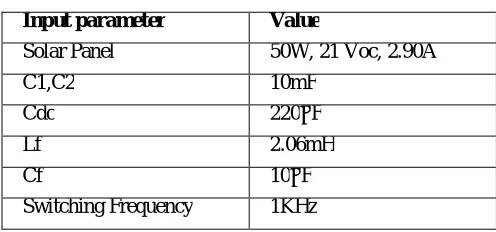
TABLE I. INPUT PARAMETERS
Input parameter Value
Solar Panel 50W, 21 Voc, 2.90A
C1,C2 10mF
Cdc 220μF
Lf 2.06mH
Cf 10μF
Switching Frequency 1KHz
FIG.9 OUTPUTVOLTAGEANDOUTPUTCURRENTWAVEFORMMICRO-INVERTERWITHSIMPLEBOOSTTECHNIQUE.
It should be noted that the harmonics are located at the switching frequency and multiples of the switching frequency. The switching frequency was intentionally set at 1 KHz so it would be rather distant from the 50 Hz fundamental frequency.
This would allow for a high cutoff frequency, which allows for small LC components. An L-C low-pass filter was
chosen for the power inverter. The value of the L is 2.06mH and the value of C is 10μF. The total harmonics
distortions obtain using above techniques are 3.20% for simple boost method, 4.73% for maximum boost method and 3.15 % for maximum constant boost with third harmonic injection.
FIG10OUTPUTVOLTAGEANDOUTPUTCURRENTWAVEFORMMICRO-INVERTERWITHMAXIMUMBOOSTTECHNIQUE.
FIG11OUTPUTVOLTAGEANDOUTPUTCURRENTWAVEFORM MICRO-INVERTERWITHMAXIMUMCONSTANTBOOSTWITH
THIRDHARMONICINJECTIONTECHNIQUE.
V. CONCLUSION
This paper proposed the simulation of micro-inverter with the different control techniques. The dual stage topology has been used. In dual-stage inverters, the DC voltage rising circuit and DC/AC voltage inverting circuit would be decoupled. The Half Bridge Push Pull DC-DC converter is used and H Bridge Inverter is use for DC-AC converter. The output of Micro-inverter is 230V AC rms is obtained in two techniques. While in maximum boost the desired output voltage is not obtained. Taking a look to the end results, the control techniques are discussed among which we observe that that the carrier frequency for controlling technique is 1 KHz. The total harmonics distortion in third harmonic injection method is less and the voltage gain is more as compare to other.
REFERENCES
[1] David M. Scholten, N. Ertugrul And W. L. Soong ( 2013) “Micro-Inverters In Small Scale Pv Systems: A Review And Future Directions”, Australasian Universities Power Engineering Conference, AUPEC 2013, Hobart, Tas, Australia.
[2] Tahsina Hossain Loba, Khosru M Salim, “Design And Implementation Of A Micro Inverter For Single PV Panel Based Solar Home System”, Informatics, Electronics & Vision (ICIEV), 2013 International Conference, IEEE 2013
[3] Viranchi Pandya , A.K. Agarwala, “ Diagonal Pv Micro-Inverter With Isolated Output”, Power Electronics (IICPE), 2012 IEEE 5th India International Conference, IEEE 2012
[4] Bhaskar, M.A.; Vidya, B.; Madhumitha, R.; Priyadharcini, S.; Jayanthi, K.; Malarkodi, G. R. (2011, March). A Simple Pv Array Modeling Using Matlab. International Conference On Emerging Trends In Electrical And Computer Technology (ICETECT), 2011, IEEE
[5] Duo Li, Zhw Zhang, Biwen Xu, Min Chen, Zhaoming Qian, “A Method Of Power Decoupling For Long Life Micr-Inverter”, IECON 2011 - 37th Annual Conference On Ieee Industrial Electronics Society, IEEE 2011
[6] Huang-Jen Chiu; Yu-Kang Lo ; Chun-Yu Yang ; Shih-Jen Cheng ; Chi-Ming Huang ; Ching-Chun Chuang ; Min-Chien Kuo ; Yi-Ming Huang ; Yuan-Bor Jean; Yung-Cheng Huang, “A Module-Integrated Isolated Solar Microinverter” , IEEE Transactions On Industrial Electronics, Vol. 60, No. 2, Feb.2013
[7] B.Y. Husodo, M. Anwari, And S.M. Ayob, “Analysis And Simulations Of Z-Source Inverter Control Methods”, IPEC 2010, IEEE.