ISSN: 2319-8753
I
nternational
J
ournal of
I
nnovative
R
esearch in
S
cience,
E
ngineering and
T
echnology
(An ISO 3297: 2007 Certified Organization)
Vol. 3, Issue 10, October 2014
Simulation Study of A Grid Connected Hybrid
Pulse Width Modulated Multi-Level Converter for
A Distributed Power Generation
Omeje, C. O.1, Esobinenwu, C.S.2
Lecturers, Department of Electrical Engineering, University of Port Harcourt, Rivers State, Nigeria1,2
ABSTRACT: The quest for efficient power and energy sustainability has been of utmost importance to technological development. Power generation, transmission and distribution undeniably have been impeded by inherent harmonic distortions emanating from power lines and power devices. The attenuation of this harmonic is made possible using appropriate power semiconductor device. This paper therefore detailed a complete analysis of a grid connected hybrid pulse width modulated multi-level converter applied in a distributed power generation. The stage by stage dc power conversion from the photovoltaic supply in relation to the solar irradiance at different operating temperature of photovoltaic (PV) radiation is presented in this work. A mathematical modeling and Simulink block modeling of a d.c boost converter needed for increasing the PV output voltage to appreciable magnitude is incorporated. A follow up is a complete model of the hybrid five level a.c converter which is formed by a cascade of three level flying capacitor and H-bridge inverter modulated with the conventional multi-carrier sinusoidal method of pulse-width modulation at 0.8 modulation index. The synchronization of the multilevel a.c converter output voltage with the utility was actualized using the inductor current interface. A computer simulation of the proposed model was carried out in MATLAB/SIMULINK and the corresponding results were presented for analysis.
KEY WORDS: Photo Voltaic System, Solar maximum power point tracker, Boost Converter, Hybrid Multi Level Converter Topology, Multi-carrier sinusoidal pulse width modulation, Utility Interface and harmonic distortion.
I. INTRODUCTION
Over the years, electricity generation has largely depended on fossil fuel as its major source of production. Most recently, the hazardous effects that accompany the use of fossil fuel in power generation have drawn much needed attentions to the global and innovative scientific approach. The drastic impacts of indiscriminate air pollution with an unavoidable threat to global warming, as a result of degradation of ozone layer and the restricted reserve of fossil fuel sources followed by the increasing cost of fossil fuel based electricity generation, has necessitated the urgent need for an alternate form of electricity source of generation. The renewable energy supply with solar (photovoltaic) has crept in leaps and bounds in most residential, administrative offices and micro-industrial power applications as the most reliable substitute for fossil fuel due to its inherent environmental friendliness, its harmless effect to the ecosystem and its simplicity in the mode of operation and maintainability.
Distributed generation (DG) consist of a number of small and medium power generation systems connected to the distribution grid feeding a dedicated consumer with a part of its power supplied to the grid [1]. A distributed power generation that is energized through a renewable energy source involves the interconnection of power electronic converters to a solar energy supply which is interfaced with utility or grid system. This scheme has made progress in recent time in the analysis, generation and control of power supply to local load consumers.
II. RELATED WORK
ISSN: 2319-8753
I
nternational
J
ournal of
I
nnovative
R
esearch in
S
cience,
E
ngineering and
T
echnology
(An ISO 3297: 2007 Certified Organization)
Vol. 3, Issue 10, October 2014
polluted current to the grid under discontinuous conduction. In [4], there is a pronounced phase shift between the filtered inverter current and the grid voltage. Therefore, a power factor much less than unity was realized due to the presence of harmonics thus reducing the expected output power resulting from a decreased output voltage level due to high current. Analysis of a fixed band and sinusoidal hysteresis current controller for voltage source inverters is reported in [5]. It is observed from this report that the mode of modulation employed was mainly the upper and lower fixed band hysteresis for controlling the switching pattern of the converter thus limiting this scheme to a single phase which is also prone to harmonic.
III. METHODOLOGY
A grid connected pulse width modulated multi-level inverter involves the application of power semiconductor circuit devices in the generation and regulation of current electricity to an appreciable value of unity power factor. A grid connected inverter usually consists of a photovoltaic array, a boost converter device, a single or three phase inverter, a power filter and an interface unit which most time contains an interfacing inductor. The block diagrams shown in figures 1a and 1b depict a complete set up for a three phase grid connected inverter which formed the basis of this study methodology.
Figure 1a: Block Diagram of a Grid connected PV Inverter.
Figure 1b: A Hybrid Diagram of a Grid connected PV Inverter.
1.0 Photovoltaic System Components
.
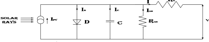
Photovoltaic module is set up from the formation of strands of solar cells that convert the solar energy of the sun to electric power of utilizable magnitude [6]. A photovoltaic system is commonly modeled using the Shockley diode which can be found in most solar energy literature. The complete circuit diagram of a photovoltaic system is as shown in figure 2.
Figure 2: Circuit Diagram of a photovoltaic system.
P.V Supply Boost
Converter
3-Phase Inverter
Filter Circuit
Inductive Load
Grid Supply
ISSN: 2319-8753
I
nternational
J
ournal of
I
nnovative
R
esearch in
S
cience,
E
ngineering and
T
echnology
(An ISO 3297: 2007 Certified Organization)
Vol. 3, Issue 10, October 2014
The model of the solar cell can be realized by considering an equivalent circuit of solar cell which consists of a current source in parallel with a diode, capacitor and shunt resistor as shown in figure 3.
Figure 3: Equivalent Circuit of a solar cell.
The solar cell voltage is been represented as the output voltage (v) in volt which is also dependent upon the solar
irradiance and the magnitude of the ambient solar cell temperature.
The p.n junction of the semiconductor in figure 2 has a depletion layer capacitance which is typically neglected in the
modeling of solar cells. Thus, Icis zero under this condition [7]. The following photovoltaic equations represented in
(1) – (6) are very essential in the determination of the Solar maximum power point tracker [7].
I = I e −1 (1)
I = (V + IR )
R (2)
I = I − I − I (3)
Substituting (1) and (2) into (3) results to (4) as shown
I = I − I e −1 − (V + IR )
R (4)
V =KT
q ln 1−
I−I
I (5)
P = V × I (6) I = Solar cell current (A),I = Light generated current (A) I = Diode saturation current (A)
q = Electron charge( 1.6 × 10 C), K = Boltzmann constant (1.38 × 10 J/K),
T = Cell temperature in kelvin; V = solar cell output voltage in volt,
R = Solar cell series resistance (Ω), R = Solar cell shunt resistance (Ω),
I = diode current (A) and I = short circuit current (A).
Equations (1) – (5) were modeled in MATLAB. A hybrid polycrystalline PV panel was used as already shown in figure 1b. The ratings of the PV panel include the followings:
Maximum power P = 150 w, maximum current I = 4.5 A, short circuit current
I = 4.75A and open circuit voltage V = 43.5V.
The maximum power point tracking was achieved graphically using (1)-(5). The result presented in figures 4a and 4b represent the P-V and I-V characteristics of the photovoltaic system at different temperature ranges of 25 and
50 at varying solar irradiance. It is observed in figures 4a and 4b that the magnitudes of power and current increase
ISSN: 2319-8753
I
nternational
J
ournal of
I
nnovative
R
esearch in
S
cience,
E
ngineering and
T
echnology
(An ISO 3297: 2007 Certified Organization)
Vol. 3, Issue 10, October 2014
Fig.4a P-V curve at varied solar irradiance Fig.4b I-V curve at varied solar irradiance.
2.0 Boost Converter and mode of operation.
Boost converter is a power electronic device that converts an unregulated input voltage to a regulated output voltage such that the magnitude of the corresponding output voltage is appreciably higher than the supply voltage. The boost converter as reported by many references can operate in continuous and discontinuous current mode depending on the values of the passive components chosen as well as the duty cycle of the converter.
In a continuous current conduction operation, the active switch in figure 5 is turned on at t = 0 with the diode D1 been
reverse biased by an inductor current IL1.
At a time interval of 0≤t≤DT, the source voltage (48v) is impressed on the inductor such that = in this interval, the inductor current rises from its initial value of IL1 to IL2. The change in the inductor current in terms of the
duty cycle and operating frequency is given by (7)
∆ = − = = ×
× (7)
At an interval of DT≤t≤T the switch is turned off. The impressed voltage across the inductor becomes the voltage
difference between the source and the output. At this point, the inductor current falls linearly from IL2 to IL1. The
change in the inductor current in terms of the duty cycle and operating frequency is therefore represented by (8)
∆ = − = ( ) ( )
× (8)
The simplification of (7) and (8) gives rise to the general boost converter voltage equation in (9).
= 1
1− (9)
Where D = converter duty cycle, = converter output voltage (220v), = supply voltage (48v), F = supply frequency
(50Hz) = minimum inductance. The components values for the boost converter used in this analysis are presented in
figure 5 with a duty cycle of 0.5 while the input and output voltages are shown by the simplorer results in figures 6a and 6b respectively.
Fig. 5 Boost Converter Circuit
0 5 10 15 20 25 30 35 40 45 50
0 20 40 60 80 100 120 140 160 180
BP SX 160S Photovoltaic Module P-V Curve at different solar irradiation
Module voltage(V)
M
o
d
u
le
p
o
w
e
r(
W
)
G1=1Kw/m2
G2=0.8Kw/m2
G3=0.6Kw/m2
G4=0.4Kw/m2
G5=0.2Kw/m2
0 5 10 15 20 25 30 35 40 45 50
0 0.5 1 1.5 2 2.5 3 3.5 4 4.5 5
Photovoltaic Module I-V Curve at different solar irradiation
Module voltage(V)
M
o
d
u
le
c
u
rr
e
n
t(
A
)
G1=1Kw/m2
G2=0.8Kw/m2
G3=0.6Kw/m2
G4=0.4Kw/m2
G5=0.2Kw/m2
+ V
+ V
D1
40m F 48 V
0.4m H
R1 20 Ohm
VM1 40m F PWM VM2
ISSN: 2319-8753
I
nternational
J
ournal of
I
nnovative
R
esearch in
S
cience,
E
ngineering and
T
echnology
(An ISO 3297: 2007 Certified Organization)
Vol. 3, Issue 10, October 2014
Fig.6a Boost Input Voltage
Fig.6b Boost Output Voltage.
3.0 Multi level Converter and Multi-Carrier Pulse-Width Modulation
Multi-level converters have formed an essential tool in different respects and have gained enormous attentions in the industries and academic research institutes as one of the preferred choices of power electronic converters for high power and high voltage applications [9]. Multi-level converter from the modular viewpoint is an inverter topology that has a voltage level above two voltage states. Currently, multi-level converters are commercialized in standard and customized products that can sustain a wide range of applications such as compressors, extruders, pumps, fans, grinding mills, rolling mills, conveyors, crushers, blast furnace blowers, flexible alternating current (FACTS-DEVICES), gas turbine starters, mixers, mine hoists, reactive power compensations on high voltage direct current (HVDC) transmission, marine propulsion devices, hydro pumped storage device, wind energy conversion, induction motor drives and railway traction applications [10-16]. The major significance of this work, in addition to grid voltage and frequency synchronization, is to propose a fault tolerant five-level inverter topology that enhances a D.C capacitor
voltage balance strategy which reduces the capacitor voltage drift (dvdc /dt) associated with other multi-level topologies.
This study is also meant to generate a five-level inverter topology that has a reduced switching loss. It can operate as a fault-tolerant inverter by producing optimum five-level voltage in the absence of fault and a three-level voltage during fault occurrence at the H-bridge. A complete circuit diagram of the proposed topology is shown in the appendix.
In the proposed five-level topology, the In-phase disposition modulation scheme (IPD) was adopted. The realization of
this scheme was done by comparing the modulating /reference signal at the fundamental frequency value with four triangular carrier waves having higher switching frequency than the modulating signal and in phase with it but with different offset voltage values. The carrier to fundamental frequency ratio or the frequency modulation index for this
topology was adopted to be = for better performance of the proposed multi-level PWM.
The operational principles of the proposed five-level inverter can be explained as follows:
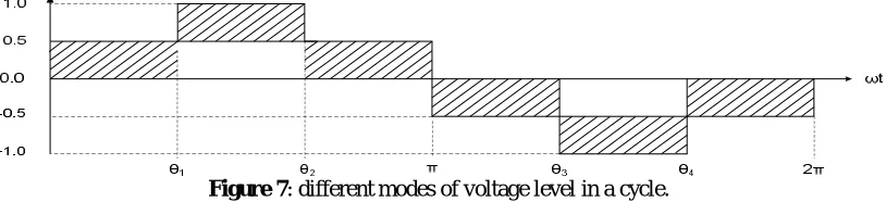
For one cycle of the fundamental frequency, the proposed multilevel operates through four (4) different modes as illustrated in figure 7.0
Figure 7: different modes of voltage level in a cycle.
Mode 1: 0≤ωt≤θ and θ ≤ ωt ≤ π
Mode 2: θ ≤ ωt ≤θ
Mode 3: π≤ωt≤θ and θ ≤ ωt ≤ 2π
Mode 4: θ ≤ ωt ≤θ
The switching process varies comparatively with these four modes and the corresponding modulation index. 0
300.00
100.00 200.00
39.00m 40.00m
BOOST OUTPUT VOLTAGE (Volts)
VM2....
40.00 55.00
45.00 50.00
39.00m 40.00m
BOOST INPUT VOLTAGE (Volts)
ISSN: 2319-8753
I
nternational
J
ournal of
I
nnovative
R
esearch in
S
cience,
E
ngineering and
T
echnology
(An ISO 3297: 2007 Certified Organization)
Vol. 3, Issue 10, October 2014
For M ≤0.5, 0≤ωt≤θ and θ ≤ ωt ≤ π. T3 is compared with the reference signal to produce a firing pulse
for of the three-level flying capacitor cascaded to H-bridge inverter.
For M ≤1.0,θ ≤ ωt ≤θ . T4 is compared with the reference signal to produce a triggering pulse for of the
H-bridge cascaded to the three-level flying capacitor.
For M ≤ −0.5,π≤ωt≤θ and θ ≤ ωt ≤ 2π. T2 is compared with the reference signal to produce a firing pulse
for of the three-level flying capacitor cascaded to H-bridge inverter.
For M ≤ −1.0, θ ≤ ωt ≤θ . T1 is compared with the reference signal to produce a triggering pulse for of the
H-bridge cascaded to the three-level flying capacitor.
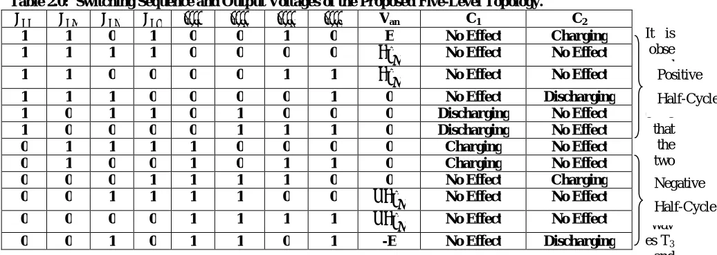
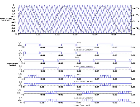
Conversely, S , S , S and S switches are complementary to , , and . They are respectively fired by
the corresponding logical switching functions shown in table 2. Figure 8.0 represents the eight switching pulses produced at phase A when the four carrier signals are compared with the reference or modulating wave.
Table 2.0: Switching Sequence and Output Voltages of the Proposed Five-Level Topology.
It is obse rved from figur e 8
that the two inner trian gular
wav es T3
and
T2 are used to control the modulation of the three-level flying capacitor while the remaining two outer triangular waves
T4 and T1 are used to control the modulation of the H-bridge cascaded with the three-level flying capacitor inverter.
The triangular carrier waveforms used in this modulation were assigned the following offset voltage values during the modulation process:
= [0 0.5 0]
= [−0.5 0 −0.5]
Triangular carrier off set value for the 3-level FCC inverter
= [0.5 1 0.5]
= [−1 −0.5 −1]
Triangular carrier off set value for the H-bridge cascaded inverter
The sinusoidal equations used as a modulating signal for the reviewed three phases, multi-level converters are presented as follows:
V = √ × × sin (10)
V =
√ × × sin − (11)
V = √ × V × sin − (12)
Van C1 C2
1 1 0 1 0 0 1 0 E No Effect Charging
1 1 1 1 0 0 0 0 No Effect No Effect
1 1 0 0 0 0 1 1 No Effect No Effect
1 1 1 0 0 0 0 1 0 No Effect Discharging
1 0 1 1 0 1 0 0 0 Discharging No Effect
1 0 0 0 0 1 1 1 0 Discharging No Effect
0 1 1 1 1 0 0 0 0 Charging No Effect
0 1 0 0 1 0 1 1 0 Charging No Effect
0 0 0 1 1 1 1 0 0 No Effect Charging
0 0 1 1 1 1 0 0 − No Effect No Effect
0 0 0 0 1 1 1 1 − No Effect No Effect
0 0 1 0 1 1 0 1 -E No Effect Discharging
Negative
Half-Cycle Positive
ISSN: 2319-8753
I
nternational
J
ournal of
I
nnovative
R
esearch in
S
cience,
E
ngineering and
T
echnology
(An ISO 3297: 2007 Certified Organization)
Vol. 3, Issue 10, October 2014
Figure 8: Eight Switching Signals for the Proposed Five-Level Topology Using SPWM.
IV. SIMULATION RESULTS AND DISCUSSIONS
Simulations carried out on the proposed grid connected multilevel topology indicate an excellent performance of the hybrid network arrangement. Figure 10 depicts a three phase grid voltage and the corresponding inductor current while the proper interface of the two is presented in figure 11 as shown below. It is prominently observed in figures 10 and 11 that the inductor current attains a nearly unity power factor with the grid connected voltage thus in quasi-phase with each other.
Fig 9: Three Phase Grid Voltage and Inductor current output.
0 0.01 0.02 0.03 0.04 0.05 0.06
-1 -0.8 -0.6 -0.4 -0.2 0 0.2 0.4 0.6 0.8 1 TIME (SECOND) AMPLITUDE (VOLTS) T1 T2 T3 T4
0 0.01 0.02 0.03 0.04 0.05 0.06
0 0.5
1
1.5 SA1
0 0.01 0.02 0.03 0.04 0.05 0.06
0 0.51
1.5 SA1-COMPLEMENT
0 0.01 0.02 0.03 0.04 0.05 0.06
0 0.5
1
1.5 SA2
0 0.01 0.02 0.03 0.04 0.05 0.06
0 0.51
1.5 SA2-COMPLEMENT
0 0.01 0.02 0.03 0.04 0.05 0.06
0 0.5
1
1.5 SA3
0 0.01 0.02 0.03 0.04 0.05 0.06
0 0.51
1.5 SA3-COMPLEMENT
0 0.01 0.02 0.03 0.04 0.05 0.06
0 0.51
1.5 SA4
0 0.01 0.02 0.03 0.04 0.05 0.06
0 0.51 1.5 Time (second) Amplitude (Volts) SA4-COMPLEMENT
0 0. 01 0. 02 0. 03 0. 04 0. 05 0. 06 0. 07 0.08
-200 -100 0 100 200
Three Phase Grid Volt age (V)
0 0. 01 0. 02 0. 03 0. 04 0. 05 0. 06 0. 07 0.08
-40 -20 0 20 40 Time(second) G ri d V o lt a g e (V ) a n d I n d u c to r C u rr e n t( A )
ISSN: 2319-8753
I
nternational
J
ournal of
I
nnovative
R
esearch in
S
cience,
E
ngineering and
T
echnology
(An ISO 3297: 2007 Certified Organization)
Vol. 3, Issue 10, October 2014
Fig10: Three Phase Grid Voltage and Inductor current interfaced.
Fig 11: Phase A THD inductor filtered grid current Fig 12: Phase B THD inductor filtered grid current
Fig 13: Phase C THD inductor filtered grid current
A unique characteristic of this hybrid multi-level topology which is fault tolerance is also conspicuously observed in figures 14-16 representing phase current, phase and line voltages.
The dynamic response to fault is an excellent feature adapted to the grid operation. When a three-phase to ground fault is applied to the proposed topology when operating at its steady state condition at a transition period of 0.04s to 0.118s. It is observed that at pre-fault condition from zero to 0.117s, the inverter generates a full five-level voltage value. During fault condition between 0.04s to 0.118s, the inverter voltage depletes to a three level voltage value but does not entirely reduce to zero voltage and at post-fault period ranging from 0.119 to 0.160s, the inverter regains its full five-level voltage production capacity as depicted in figures 14, 15, and 16 respectively. This unique but dynamic behaviour of this converter confirms the peculiarity of this topology to a fault associated condition. The Simulink diagram is presented in the appendix.
0 0.01 0.02 0.03 0.04 0.05 0.06 0.07 0.08
-200 -150 -100 -50 0 50 100 150 200 TIME (second) G ri d V o lt a g e /I n d u c to r C u rr e n t
0 0.01 0.02 0.03 0.04 0.05 0.06 0.07 0.08
-20 0 20
Time (s)
0 200 400 600 800 1000
0 20 40 60 80 100 120 Frequency (Hz)
Fundamental (50Hz) = 23.7 , THD= 1.26%
M a g ( % o f F u n d a m e n ta l)
0 0.01 0.02 0.03 0.04 0.05 0.06 0.07 0.08
-20 0 20
Time (s)
0 200 400 600 800 1000
0 20 40 60 80 100 120 Frequency (Hz)
Fundamental (50Hz) = 23.7 , THD= 1.28%
M a g ( % o f F u n d a m e n ta l)
0 0.01 0.02 0.03 0.04 0.05 0.06 0.07 0.08
-20 0 20
Time (s)
0 200 400 600 800 1000
0 20 40 60 80 100 120
Frequency (Hz)
Fundamental (50Hz ) = 23.62 , THD= 1.30%
ISSN: 2319-8753
I
nternational
J
ournal of
I
nnovative
R
esearch in
S
cience,
E
ngineering and
T
echnology
(An ISO 3297: 2007 Certified Organization)
Vol. 3, Issue 10, October 2014
Fig.14 5-level output current at pre-fault, during-fault and post-fault condition.
Fig.15 5-level Phase Voltage at pre-fault, during-fault and post-fault condition.
Fig. 16 5-level Line Voltage at pre-fault, during-fault, and post-fault condition
V. CONCLUSION
The analysis of a photovoltaic maximum power point tracker (MPPT), boost converter and a hybrid grid connected multi-lever inverter was presented in this work. The simulations have indeed shown the functionality of the proposed topology in harmonic reduction as eminently observed in figures 11-13 with %THD values of 1.26, 1.28 and 1.30 for the three phase inductor current. This is in conformity with the advantages of multi-level converter which is harmonic reduction and improved voltage level. Similarly, the reduced current magnitudes of 23.7A and 23.62A also lead to reduced power loss as presented in the same figures 11-13 which competes favourably and more efficiently with the high current values of 125A and 98A presented in the single phase simulation result in [4]-[5]. The unique but dynamic behaviour of the converter with pertinent to a fault associated condition also confirms the peculiarity of this topology to grid connected process.
0 0.02 0. 04 0.06 0.08 0. 1 0.12 0.14 0. 16
-2 -1 0 1 2
Time (s )
0 50 100 150 200 250 300 350 400 450 500
0 50 100 150
Frequenc y (Hz ) Fundament al (50Hz) = 1.183 , THD= 10.57%
M a g ( % o f F u n d a m e n ta l)
0 0.02 0.04 0.06 0.08 0.1 0.12 0.14 0.16
-200 -100 0 100 200 Time (s)
0 50 100 150 200 250 300 350 400 450 500
0 50 100 150
Frequency (Hz) Fundamental (50Hz) = 118.5 , THD= 40.32%
M a g ( % o f F u n d a m e nta l)
0 0.02 0.04 0.06 0.08 0.1 0.12 0.14 0.16
-400 -200 0 200 400 Time (s)
0 50 100 150 200 250 300 350 400 450 500
0 50 100 150
Frequency (Hz) Fundamental (50Hz) = 204.8 , THD= 18.97%
ISSN: 2319-8753
I
nternational
J
ournal of
I
nnovative
R
esearch in
S
cience,
E
ngineering and
T
echnology
(An ISO 3297: 2007 Certified Organization)
Vol. 3, Issue 10, October 2014
VI. APPENDIX
Figure 17: Circuit Diagram of the Proposed Five-Level Inverter Topology.
Figure 18: Simulink model of the Grid connected Hybrid Multilevel Converter.
REFERENCES
[1] Kjaer, S.B., Pedersen, J.K., Blaabjer, F.A., “Review of Single-Phase Grid-Connected Inverter for Photovoltaic Modules”. IEEE Transactions on Industrial Applications, Vol. 41, No.5,pp1292-1306, September 2005.
[2]Calais, M., Myrzik, J., Spooner, T. Agelids, V.G. “Inverters for Single-Phase Grid-Connected Photovoltaic System an Overview”. IEEE Power Electronic Specialists Conference, Vol.4. Pp.1995-2000, 2002.
[3] Malesani, L. and Divian, D.M. “A Synchronized Resonant D.C Link Converter for Soft –Switched PWM”. In Proc. IEEE Annual Conf. Rec., Pp1037-1044. 1989.
ISSN: 2319-8753
I
nternational
J
ournal of
I
nnovative
R
esearch in
S
cience,
E
ngineering and
T
echnology
(An ISO 3297: 2007 Certified Organization)
Vol. 3, Issue 10, October 2014
[5] Blaabjerg, F. Chen, Z. and Kjaer, S.B. “Power Electronics as an Efficient Interface in Dispersed Power Generation Systems”. IEEE Transaction on Power Electronics. Vol.19, No.5. pp1184-1194, 2004.
[6]Masoum, M.A.S. and Dehbonei, H. “Theoretical and Experimental Analysis of photovoltaic Systems with Voltage and Current-Based Maximum Power Point Tracking”. IEEE Trans. On Energy Conversion, Vol.17, no.4, pp.514-522. 2002.
[7] Nnadi, D.B.N. Odeh, C.I. and Omeje, C. “Use of Hybrid Solar-Wind Energy Generation for Remote Area Electrification in South-Eastern Nigeria”. Journal of Energy in Southern Africa, Vol. 25, no. 2, pp.61-69. May 2014.
[8] Ko, S.H. Lee, S.R and Dehbonei, H. “Application of Voltage and Current Controlled Voltage Source Inverters for Distributed Generation System”. IEEE Trans. on Energy Conversion, Vol.21, no.3, pp. 782-792, 2006.
[9] Tolbert, L.M. and Peng, F.Z. “Multi-level Converter as a Utility Interface for Renewable Energy Systems, IEEE Proc. on Power Eng. Soc. Summer Meeting Vol.2, pp.1271-1274, July 2000.
[10] Rodriguez, J. Franquelo, L.G. Kouro, S. Leon, J.I. Portillo, R.C. Prats, M.A.M and Perez, M.A. “Multi-level Converters: An Enabling Technology for High-Power Application”. Proc. IEEE, Vol. 97, no.11, pp. 1786-1817, November, 2009.
[11]Rodriguez, J. Bernet, S. Wu, B. Pontt, J.O and Kouro, S. “Multi-level Voltage Source Converter Topologies for Industrial Medium Voltage Drives”. IEEE Trans. Ind. Electronics, Vol.54, no.6, pp.2930-2945, December, 2007.
[12] Du, Z. Tolbert, L.M. and Chiason, J.N. “Active Harmonic Elimination for Multi-level Converters”. IEEE Trans. Power Electronics, Vol. 21, no.2, pp.459-469, March 2006.
[13] Nabae, A. Takahashi, I. and Akagi, H. “A New Neutral Point Clamped PWM Inverter”. IEEE Transaction on Industrial Applications, Vol.17, no.5, pp.518-523, 1981.
[14]Xiong, L. Poh Chiang, L. Peng, W. Blaabjerg, F. Tang, Yi and Al-Ammar Essam, A. “Distributed Generation Using Matrix Converter in Renewable Power Mode”. IEEE Transactions on Power Electronics, Vol.28, no.3, pp.1072-1080. March, 2013.
[15]Holmes, D.G. and Lipo, T.A. Pulse-width Modulation for Power Converters, Principles and Practice. John Wiley and Sons Inc. New York, 2003. [16] Mohan, N. Undeland, T.M and Robbins, W.P. Power Electronics Converters, Applications and Design. 2nd edition John Wiley and Sons Inc. New York 1995.
BIOGRAPHY
Omeje, Crescent Onyebuchi received his B.Eng (Electrical Engineering) in 2004 and M.Eng (Power Electronics and Drives) in 2011 from University of Nigeria, Nsukka. He is currently a Ph.D student in the same University. His research interests are on renewable energy, power electronics converters and machine drives. He is a lecturer in the Department of Electrical Engineering, University of Port Harcourt, Rivers State, Nigeria.