ABSTRACT
GORE, CHINMAY CHAITANYA. Study of Machine Learning algorithms for their use in Semiconductor Device Model Development. (Under the direction of Dr. W. Rhett Davis.)
This research studies machine learning algorithms from viewpoint of semiconductor device modeling. It proposes a model parameter extraction method using supervised learning algorithms.
This methodology is an effort to expedite semiconductor model development flow.
In order to validate proposed methodology, experiments are performed on available Spectre® models of a 130 nm technology. Using these models, I-V characteristics are obtained for key device
geometries under different operating conditions, which can be considered as training data. Linear
and Exponential hypothesis functions are used to extract parameters from training data. First order derivatives of these equations, along with extracted parameters are used to predict device
transconductances. In order to evaluate accuracy of fit, I-V characteristics are reconstructed using
extracted parameters and Root Mean Squared Error (RMSE) is calculated between target data and reconstructed characteristics. RMSE metric is also used to assess prediction of transconductances
by both hypothesis functions.
Outcomes of experiments show inability of chosen hypothesis functions to replicate drain and gate characteristics. Long adaptation times make it difficult to identify bottleneck: wrong choice of
hypotheses functions, inefficient optimization algorithm or the approach in general. These failures
and their possible causes are discussed.
© Copyright 2015 by Chinmay Chaitanya Gore
Study of Machine Learning algorithms for their use in Semiconductor Device Model Development
by
Chinmay Chaitanya Gore
A thesis submitted to the Graduate Faculty of North Carolina State University
in partial fulfillment of the requirements for the Degree of
Master of Science
Electrical and Electronics Engineering
Raleigh, North Carolina
2015
APPROVED BY:
Dr. Brian A. Floyd Dr. Robert J. Trew
DEDICATION
"Give a man a fish and you feed him for day; teach a man how to fish and you feed him for lifetime"
BIOGRAPHY
Chinmay Chaitanya Gore earned Bachelor Of Engineering in Electronics and Telecommunication from University of Mumbai in 2013. He joined NC State University in Fall 2013 to pursue Master Of
Science in Electrical and Electronics Engineering. He interned at Nangate Inc. during Summer and
Fall 2014 semester as Standard Cell Library Development Intern. He joined RTP Design Center of Intersil Corporation from July 2015 as Design Engineer. His area of interest include Analog/RF and
Digital Circuit Design.
Along with circuits, Chinmay is fascinated by outdoor activities (hiking, sports, etc.) and is an
ACKNOWLEDGEMENTS
It takes a village to complete a thesis. I would like to take this opportunity and express my gratitude towards everyone who directly or indirectly helped me to accomplish this goal.
First of all, I would like to thank my advisor, Prof. W. Rhett Davis for his advice and encouragement
throughout this project. He has always given me great advice, correct direction and importantly, his patient ears. I would also like to thank my committee members, Prof. Brian Floyd and Prof.
Robert Trew for their constant guidance. Prof. Floyd introduced me to the amazing world of analog circuit and Prof. Trew helped me understand miracles in analog circuits’ world. I am also grateful to
ECE Department and Prof. Paul Franzon, for partially funding my reseach. I would like to thank all
faculties, DGP and all office staff at ECE Graduate Office for making these two years highly rewarding for me.
I would like to thank Mr. Jens Michelsen, Mr. Ole C. Anderson, Mr. Schlinker, Mr. Rech and Mr.
Toniolo of Nangate Inc. for the awesome internship experience. I learned a lot of things during my intern tenure which I would not have done otherwise (Gvim and Scripting). I am also grateful to all
managers, especially Mr. Brian Allen, Mr. Shawn Evans and Mr. Mehul Shah at Intersil for making
my transition from academia to industry a comfortable experience.
I would like to thank Mr. Harshad Kolte, Mrs. Sonali Kolte and Ms. Ria Kolte for being my family
away from home. Speaking of family away from home, it becomes imperative to thank all members
of my extended family, The Wolfpack. I would like to thank Anirudha, Athreya, Abhinand, Deeksha, Gaurav, Harshal, Kirti, Navya, Mrunmayee, Nischala, Saranya, Priyanka, Rashmi, Srinjoy, Sandeep
and all my football buddies for being there with me and for me. I would like to express my special
gratitude to Chinmay Tembe and Nitish Natu. I will always cherish memories we had together throughout this entire journey and years to come. Thank you guys!!
My family members Mr. Chaitanya Gore, Mrs. Madhavi Gore and Ms. Sampada Gore have
played a huge part in all my success. I am forever indebted to them. My special thanks goes to Gore, Khadilkar, Phadke, Deshpande, Kulkarni, Ghangrekar, Chandorkar, Sahasrabuddhe, Karandikar,
Raje, Britto and Ojale families, and of course, to Hardik Sir. I would also like to thank all my relatives
and friends in India for giving me warm, happy and funny memories to cherish. I would also like to thank Mr. Jon Stewart and Mr. John Oliver for helping me to keep up with things happening around
in most hilarious ways possible.
Most importantly, I would like to thank Ms. Ashwini Deshpande. You have always believed in
me, even when I doubted myself. You have always motivated me, when I thought there is no end. All
of these would not have been possible without your love, care, understanding and motivation. I would like to thank everyone whose presence in my life have helped me to be a better person
TABLE OF CONTENTS
LIST OF TABLES . . . vii
LIST OF FIGURES. . . .viii
Chapter 1 INTRODUCTION. . . 1
1.1 Introduction . . . 1
1.2 Motivation . . . 2
1.3 Outline . . . 2
Chapter 2 Device Modeling: Problem and Solution . . . 4
2.1 Introduction . . . 4
2.1.1 What is Modeling? . . . 4
2.1.2 Semiconductor Device Modeling . . . 5
2.2 Challenges . . . 7
2.3 Proposed Methodology . . . 9
Chapter 3 Machine Learning Basics. . . 10
3.1 Understanding Learning . . . 10
3.2 Making Machines Do it . . . 11
3.3 Categories of Learning Problem . . . 11
3.4 Nomenclature . . . 12
3.5 Overview . . . 13
3.5.1 Unsupervised Learning Algorithms . . . 13
3.5.2 Supervised Learning Algorithms . . . 14
3.5.3 Deep Learning Algorithm . . . 15
Chapter 4 Experimentation. . . 17
4.1 Generation of Test Data . . . 19
4.1.1 Selection of Test Device Geometries . . . 19
4.1.2 Region Specific Modeling . . . 19
4.2 Implementation of Learning Algorithm . . . 20
4.3 Validation . . . 24
Chapter 5 Results . . . 25
5.1 Strong Inversion Region Modeling . . . 26
5.2 Moderate Inversion Modeling . . . 34
5.3 Weak Inversion Region Modeling . . . 40
5.4 Interpretation Of Results . . . 47
Chapter 6 Conclusion . . . 48
6.1 Critical Analysis . . . 48
6.1.1 Choice of Hypothesis Function . . . 48
6.1.3 Temperature and Layout Dependent Effects . . . 50
6.1.4 Choice of Optimization Algorithm . . . 50
6.2 Conclusion . . . 50
LIST OF TABLES
Table4.1 Process Specific Dimensions . . . 19
Table5.1 Linear Hypothesis Function in Strong Inversion . . . 26 Table5.2 Exponential Hypothesis Function in Strong Inversion . . . 27 Table5.3 Drain Transconductance RMSE Comparison of Hypotheses Functions - Strong
Inversion . . . 27 Table5.4 Linear Hypothesis Function in Moderate Inversion . . . 34 Table5.5 Exponential Hypothesis Function in Moderate Inversion . . . 34 Table5.6 Drain Transconductance RMSE Comparison of Hypotheses Functions -
Mod-erate Inversion . . . 35 Table5.7 Linear Hypothesis Function in Weak Inversion . . . 40 Table5.8 Exponential Hypothesis Function in Weak Inversion . . . 40 Table5.9 Drain Transconductance RMSE Comparison of Hypotheses Functions - Weak
LIST OF FIGURES
Figure2.1 Classification of Semiconductor Device Models[21] . . . 6
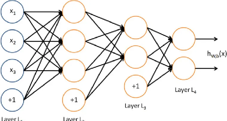
Figure3.1 Deep Learning Network Example . . . 16
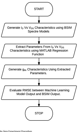
Figure4.1 Step-by-Step Experiment Procedure . . . 18
Figure4.2 Overview of Regression with Gradient Descent Algorithm . . . 23
Figure5.1 NMOS Wide/Long Drain Characteristics in Strong Inversion . . . 28
Figure5.2 NMOS Wide/Short Drain Characteristics in Strong Inversion . . . 29
Figure5.3 NMOS Narrow/Short Drain Characteristics in Strong Inversion . . . 30
Figure5.4 NMOS Wide/Long Drain Transconductance in Strong Inversion . . . 31
Figure5.5 NMOS Wide/Short Drain Transconductance in Strong Inversion . . . 32
Figure5.6 NMOS Narrow/Short Drain Transconductance in Strong Inversion . . . 33
Figure5.7 NMOS Wide/Long Drain Characteristics in Moderate Inversion . . . 35
Figure5.8 NMOS Wide/Short Drain Characteristics in Moderate Inversion . . . 36
Figure5.9 NMOS Narrow/Short Drain Characteristics in Moderate Inversion . . . 37
Figure5.10 NMOS Wide/Long Drain Transconductance in Moderate Inversion . . . 37
Figure5.11 NMOS Wide/Short Drain Transconductance in Moderate Inversion . . . 38
Figure5.12 NMOS Narrow/Short Drain Transconductance in Moderate Inversion . . . . 38
Figure5.13 NMOS Wide/Long Drain Characteristics in Weak Inversion . . . 41
Figure5.14 NMOS Wide/Short Drain Characteristics in Weak Inversion . . . 42
Figure5.15 NMOS Narrow/Short Drain Transconductance in Weak Inversion . . . 43
Figure5.16 NMOS Wide/Long Drain Transconductance in Weak Inversion . . . 44
Figure5.17 NMOS Wide/Short Drain Transconductance in Weak Inversion . . . 45
CHAPTER
1
INTRODUCTION
1.1
Introduction
This research studies machine learning algorithms from the perspective of semiconductor device model parameter extraction. It aims to propose a generic, simple yet accurate methodology for
parameter extraction flow.
The hypothesis behind this research is that semiconductor device modeling problem can be
treated like Data Mining problem. Electrical characteristics of the device such as I-V and C-V
char-acteristics represent input-output relationship, which can be modeled by convoluted mathematical functions. This research is based on the hypothesis that supervised machine learning algorithms
can be used for development of such complex model equations. Since full model development
flow is an extensive task, efforts are concentrated on the parameter extraction step in the model development flow.
Experiments are designed in order to validate the hypothesis that supervised machine learning
can be used to extract useful information i.e. model equation parameters from measured data. In order to expedite development of the methodology, I-V characteristics data generated by computer
simulations is considered as reference and used as training data for supervised machine learning
1.2. MOTIVATION CHAPTER 1. INTRODUCTION
functions and extracted values of function parameters, an attempt is made to replicate I-V character-istics so that Root Mean Squared Error (RMSE) between training data and replicated charactercharacter-istics
is acceptable. Additionally, RMSE between first order derivatives of training data and model outputs
is also evaluated. For ease of comparison, graphs of experiment outcomes are also provided. Outcomes of experiments expose flaws and bottlenecks in this methodology. Supervised
ma-chine learning algorithms chosen can replicate only a small subset of I-V characteristics. Due to
simplistic nature of hypothesis functions and optimization algorithm, experiments were often hindered by long adaptation times. All these shortcomings, with their possible causes and remedies
are documented in chapter 6. This research is a feasibility study for the proposed approach and can
serve as a starting point for future research endeavors.
1.2
Motivation
Semiconductor device modeling is an area of extensive research. Technology Computer Aided Design (TCAD) models are used to design and analyze semiconductor devices. They are also used as
first step in compact model development. Compact models are used for circuit design and functional
verification. Accuracy of these models directly translates to design accuracy, high yield and more profit.
However, development of TCAD and compact models is a huge undertaking. It requires concrete
understanding of underlying physics. It also requires a lot of simulation resources (computation time and memory), making it very complex and expensive. Additionally, models developed for one
device cannot be ported i.e. used for other device, if governing physical principles of two devices
are different.
This research is motivated by the need of acceleration of model development for semiconductor
devices. Research efforts have been directed in semiconductor device modeling and machine
learning fields separately, however, the use of machine learning in device modeling is yet to be explored by research community. Earlier work[11]uses Artificial Neural Network (ANN) approach
for region specific CMOS modeling. This research is inspired by a similar philosophy, however it
uses different building blocks.
1.3
Outline
The organization of this thesis is as follows: Chapter 2 introduces readers to current semiconductor model development methodologies and explains their shortcomings with respect to CMOS
1.3. OUTLINE CHAPTER 1. INTRODUCTION
overview of experimentation done in order to validate proposed hypothesis and implementation of algorithms. Chapter 5 presents results obtained with their interpretation while chapter 6 elucidates
CHAPTER
2
DEVICE MODELING: PROBLEM AND
SOLUTION
2.1
Introduction
2.1.1 What is Modeling?
A model can be thought of as a mathematical equation that governs behavior of a particular sys-tem. Model equations can be of various types, including but not restricted to dynamical systems,
statistical models, differential equations. It is also possible that these given types of models can overlap, depending on abstractions in context. Use of models spans across various disciplines, such
as natural sciences (physics, chemistry, biology, astronomy, etc.), social sciences (psychology,
soci-ology, economics, etc.) and importantly, engineering disciplines (artificial intelligence, electronics engineering, acoustic engineering, etc.).
Models are used to capture effects which contribute to behavior of system under investigation.
Many times, they are used to predict system response for unknown input stimuli. Stochastic (one or more input variables are of random nature) models are capable of modeling effects of random input
2.1. INTRODUCTION CHAPTER 2. DEVICE MODELING: PROBLEM AND SOLUTION
the input variables are deterministic and some are random in nature). It is expected that models should be generalizable, that is models should take into account as many effects as possible, so that
they can be used accurately over broad input space. Models exhibit trade-off between accuracy and
simplicity. Complex models have more predictive power, however they are difficult to understand and analyze.
Based on availability of information while developing models, they are broadly classified as
black-box, white-box and grey-box models. White-box model is a model where all necessary system information was available at its inception. On the other hand, if there is no significant prior
infor-mation available which can be used while developing the model, model is then termed as black-box
model. In reality, there are no models which are purely theoretical (white-box) or without prior information (black-box). They are called grey-box models, which are based on theoretical stuctures
and use test data for completing development[26].
It is imperative to assess model quality prior its deployment. There are multiple ways in which models can be evaluated. Three key aspects of model evaluation closely related to this research are:
1. Fit to Empirical Data: Outcomes of model are compared to actual measured data. Error metrics
such as root mean squared error (RMSE) can be used to quantify model fitness.
2. Model Scope: Model has to be checked for interpolation and extrapolation. Interpolation
means ability to describe system behavior between two known data points. Extrapolation means ability to describe system behavior for data points which are out of known bounds.
3. Numerical Stability: Many applications of model require their implementation in a computer
solver software. In order for solver software programs to perform correctly, model must be
checked for stability and boundaries of unstable operations must be known beforehand.
2.1.2 Semiconductor Device Modeling
A semiconductor device model is often an equation that relates terminal voltages and node currents
through mathematical functions. These models are used to reproduce/predict electrical
charac-teristics of semiconductor devices. They capture electro-physical behavior as a function of device geometry, biasing conditions, environmental factors such as temperature and also, process
varia-tions[9]. As put forth by Schneider and Galup-Montoro[19], semiconductor device models serve
as the fundamental link between design engineers and foundries, assisting to transform process properties into applications. Semiconductor device models allow computer simulation of circuits
2.1. INTRODUCTION CHAPTER 2. DEVICE MODELING: PROBLEM AND SOLUTION
Figure 2.1Classification of Semiconductor Device Models[21]
As explained in subsection 2.1.1, models can be developed for different levels of abstraction.
Semiconductor device models are primarily developed for:
1. Device Design and Analysis Models
2. Device Models for circuit simulation
Figure 2.1 decscribes broad classification of semiconductor models. Models used for design and
analysis of devices are called TCAD models. These models refer to fabrication process and hence
are most accurate. These models can provide insight into details of device operation and hence are very useful for device optimization for performance. However, large memory usage and long
computation time prohibit their usage in circuit design flow.
For use in circuits with sea-of-devices, simulation models are required which are accurate, yet faster than TCAD models. These models are called Compact Models, used extensively for circuit
design and functional verification. Tsividis and Andrews[21]have given guidelines pertaining
2.2. CHALLENGES CHAPTER 2. DEVICE MODELING: PROBLEM AND SOLUTION
1. Models should meet common requirements of digital circuits such as I-V characteristics, leakage currents, intrinsic and extrinsic capacitances, charges, etc.
2. Models should be continuous. This means not only charges and currents should be continuous
with respect to each terminal voltages, but even their derivatives should be continuous.
Com-mercial circuit simulator often use non-linear KCL and Newton-Raphson method based on linearization, which requires continuous derivatives for effective operations. Also, distortion
analysis accuracy depends on continuity of higher-order derivatives.
3. Model formulation and model parameters must be strictly physical. Results of model should
make physical sense. Model should not exhibit unphysical behavior such as generating power and negative transconductances or capacitances.
4. Model should account for all intrinsic and extrinsic parasitic elements which alter circuit performance.
5. Model should account for temperature and layout dependent effects.
6. Model must be numerically robust and computationally effective.
2.2
Challenges
In order to explain common challenges faced during the process of semiconductor device modeling, the widely used CMOS technolgy is used as an example. As predicted by Moore’s Law[16]and ITRS
guidelines[10], the feature size of CMOS transistors approximately shrinks by a factor ofp2 per
year. This results in approximately 2 times increase in number of transistors per unit area. Also, smaller geometries reduce transit time and hence an increase in the fundamental frequency,fT ,
by factor of 2 is observed. Since the cost of wafer remains almost same, this 2X increase in speed
and 2X decrease in area results in overall cost reduction. It is roughly estimated that there is 30% improvement in cost per function every year. This is a strong economic impetus, often suggesting
that Moore’s Law is also a law of semiconductor economics.
However, shrinking feature sizes have severely altered behavior of modern CMOS devices. Effects
which could be neglected in previous generations are now prominently observed and have significant
impact on device behavior. If these effects are not accounted for in models, it may lead to partial or complete failure of circuits. Several key effects, also called "short channel effects" are listed below:
2.2. CHALLENGES CHAPTER 2. DEVICE MODELING: PROBLEM AND SOLUTION
2. Drain Induced Barrier Lowering (DIBL)
3. Gate Induced Drain Leakage (GIDL)
4. Velocity Saturation
5. Mobility Degradation
6. Threshold Voltage Variations
7. Random Dopant Fluctuations (RDF)
Additional TCAD simulations are required to capture these effects with accuracy. As stated in section
2.1, integrated circuit design and verification relies heavily on availability of accurate device models.
In order to capture higher order effects, scaling of devices requires complex model to accommodate as many as possible scaling imposed effects. This requires fundamental understanding of device
physics, origin of such effects. This reinstates requirement of physics based modeling, due to its
high accuracy as compared to other methods. Physics based CMOS models can be further classified into following categories[21]:
1. Threshold Voltage Based Models: BSIM3[4]and BSIM4[17].
2. Inversion Charge Based Models: ACM[7]and EKV[6] [3].
3. Surface Potential Based Models: PSP[8]and HiSIM[14]
CMOS technology is leading, but it is not the only technology in semiconductor world. For scaling beyond 32nm technology node, non-planar multi-gate devices, often referred as FinFETs are believed
to be promising solution over planar CMOS technologies. Also, geometric structure of CMOS imposes
limits on its high frequency operations. For RF and millimeter wave applications, Heterojunction Bipolar Transistors(HBT) and High Electron Mobility Transistors (HEMT) are preferred over CMOS.
Similarly, for high power applications, Insulated Gate Bipolar Transistors (IGBT) are extensively
used.
Development of model for new semiconductor device requires a lot of resources, intensive
computations and hence, requires plenty of time to develop robust model meeting above mentioned
requirements. Similar endeavors are required to model a new semiconductor device, since physical base of new device may be different from existing devices. It may be possible to use some of the
2.3. PROPOSED METHODOLOGYCHAPTER 2. DEVICE MODELING: PROBLEM AND SOLUTION
2.3
Proposed Methodology
Accuracy of model depends upon choice of conformal mathematical functions as well as accuracy
of function parameters. These parameter values must be fine tuned to achieve required degree of agreement with measured data. Parameter extraction or characterization is an important step in
model development, involving extraction of function parameters from measurements[21] [20].
There are two main approaches for parameter extraction: global optimization and local opti-mization. Global optimization aims to minimize average error between simulated and measured
data. In local optimization, parameters are extracted independently from device data, obtained
under different bias conditions. Each of these conditions correspond to a dominant effect. Global optimization method treats each parameter as a fitting parameter. It may happen that values of
parameters extracted might not be coherent with their physical intent. Parameters extracted by
local optimization may not be as accurate to result in overall good fit, but they still retain their physical meaning. BSIM3 and BSIM4 have used group device extraction strategy along with local
optimization[4] [17]. It means test data is generated under same operating conditions but devices with different geometries are used.
This research proposes a parameter extraction methodology using supervised machine learning
algorithms. Extraction approach is similar to BSIM model development, local optimization with data generated from devices with diverse geometries, operated under identical conditions. Complex
model equations can be made region specific or in other words, simplified to model only the
prominent effects for those conditions. Experiments performed evaluate ability of supervised learning algorithms to accurately predict device transconductance from measured I-V characteristics
CHAPTER
3
MACHINE LEARNING BASICS
3.1
Understanding Learning
Learning is the continuous process of benefitting from previous experiences and making decisions based on them. Learning and adapting is often regarded as the most basic form of animal intelligence.
Throughout our lifespan, the ability to learn gives us the power to adjust and adapt to new situations. The decomposition of learning process into its constituents is somewhat difficult, mainly because
of variety of processes that contribute to learning as a whole.
Here are some formal definitions of learning. According to Merriam-Webster "Learning is an activity or a process of gaining knowledge or skill by studying, practicing, being taught or
experienc-ing somethexperienc-ing". Another commonly accepted definition of learnexperienc-ing is given with respect to livexperienc-ing
organisms as "modification of behavioral tendency by experience".
Important steps in learning are remembering, adapting and generalizing. Animals recollect
being in this situation, take certain actions, and determine whether they worked or not. Should
they work, those actions will be used again, otherwise, some different actions will be considered. Generalizing is the crucial part of animal intelligence. Owing to variety of situations which arise,
it takes a great deal of intelligence to recognize similarity in different situations so that previous
3.2. MAKING MACHINES DO IT CHAPTER 3. MACHINE LEARNING BASICS
3.2
Making Machines Do it
Evolution of Machine Learning can be credited to field of pattern recognition and computational
learning theory in artificial intelligence[25]. As defined by Arthur Samuel in 1959, "Machine Learning is the field of study which gives a computer ability to learn, without being explicitly programmed".
Machine Learning is all about making computers modify or adapt their actions so that these actions
get more and more accurate[12].
Similarity between human learning and machine learning processes is remarkable. Learning
machines recognise previous encounters with current data, take some actions based on previous
experiences and evaluate whether it was successful or unsuccessful. Outcome of evaluation is stored as an experience and can be used for future generalizations.
A day to day example of Machine Learning is playing a game against a computer. Initially, it
is relatively simple to defeat computer but after lots of games, it becomes harder and harder and there comes a point when victory against computer is almost impossible. It can be concluded that
either the human player is getting worse, or computer is learning from its experiences and forming strategies against the human player. Once it learns strategies to defeat current player, it will try and
use same strategies while playing against different players in future (generalization). One historically
significant example of Artificial Intelligence is the chess computer Deep Blue, developed by IBM. It is known as the first piece of artificial intelligence to win both a chess game and a chess match
against reigning world champion under regular time controls[22].
3.3
Categories of Learning Problem
The number of problems which can be solved by Machine Learning are ever-increasing. Mohri et.
al.[15]have enumerated broad categories of problems which are addressed by machine learning
approach.
1. Classification: The outcome expected in these problems in assignment of category for every element in the data set. Classification can be done via supervised as well as unsupervised
learn-ing algorithms. A day-to-day example of classification problem is news websites where news
articles are classified as per their contents. Text Classification, Optical Character Recognition, Facial Recognition and Speech Recognition are also included in this problem subset.
2. Regression: It is the process of predicting outcomes for unknown input conditions. Known data
points consisting of input conditions and target outcomes form training data. This training
3.4. NOMENCLATURE CHAPTER 3. MACHINE LEARNING BASICS
conditions is an example of Regression problem. It usually requires Supervised Learning Algorithms.
3. Ranking: As the name suggests, ranking problem means re-arranging data elements as per
some criterion. Returning web pages in response to a search query is a commonplace example of ranking problem.
4. Clustering: Problem of clustering is somewhat analogous to classification problem. It means partitioning of data elements into homogeneous subsets. It is often used to analyze very
diverse data space. For example, in the social network analysis, clustering algorithms try and
identify "communities" with some common attributes within large and diverse population.
5. Dimensionality Reduction: This is a problem of converting multi-dimensional representation
of data into lower-dimensional representation, but preserving some properties of initial
representation. Surrogate Modeling is an example of Dimensionality Reduction problem.
3.4
Nomenclature
Before delving into technicality of Machine Learning Algorithms, it is required to introduce the reader to basic nomenclature used extensively in literature pertaining Machine Learning and Artificial
Intelligence. To elucidate these definitions, they are accompanied by an example of housing price
prediction problem.
1. Training Data: Set of data points used to tune a learning algorithm is called Training Data. It
consists of input features and their corresponding outputs. The survey of houses in a particular
locality having information such as its cost, no. of bedrooms, age, area, etc. can be thought of as training data.
2. Features: Characteristics of data points which would play a role in deciding outcome are called
features or input variables. Age of the house, no. of bedrooms, area of the house, etc. can be called features.
3. Target: Set of known outcomes which help supervised learning algorithms to adapt to data presented is called target. In this example, apartment price is the target.
4. Training Set: Set of targets and their corresponding input features is termed as training set.
3.5. OVERVIEW CHAPTER 3. MACHINE LEARNING BASICS
It contains input features and some unknowns (called as parameters). Training set is used to modify these parameters so that error between predicted output and target output is
minimized.
6. Cost Function: The function that expresses error between target outputs and outputs predicted
by hypothesis function is called cost function.
3.5
Overview
This section describes few commonly used algorithms at higher level. Details pertaining their
implementation are out of the scope of this section.
3.5.1 Unsupervised Learning Algorithms
Unsupervised Learning Algorithms are applied primarily to problems of classification nature. It is
analogous to certain learning experiences, where there is no right answer. Training data do not have "correct" responses, therefore there is no supervision on algorithms. These algorithms try to identify
similarities between input data points and categorize them together. The statistical approach to
unsupervised learning is known as density estimation.
K- means algorithm is an unsupervised learning algorithm that divides input data space into k
clusters. We assign k cluster centers to our input space, and it is expected that the cluster centers will
be at the center of their respective clusters. Clusters and their respective centers will be determined by the Learning Algorithm. In order to define center of set of points, we need to specify distance
between two points (normal Euclidean distance is very common measure). Once distance measure
is available, a central point of a set of data points can be calculated by the mean average. A safe bait to place a cluster center is at the midpoint of the cluster. Inadvertently, euclidean distance from
each data point to cluster center is getting minimized. Each data point is associated with a cluster
whose center is closest to that point.
To start with, cluster centers are randomly positioned throughout the data space. Distance
between a data point and all cluster centers is calculated and data point is assigned to cluster having
cluster center nearest to that particular data point. Once all points are assigned to available clusters, mean of every cluster is calculated and cluster center migrates to mean point. Iterations continue
until cluster centers become stationary[12]. Customer segmentation strategy often leverages unsu-pervised learning algorithms. From company’s past customer database, groups of customer based
on geography, income group, habits, payment methods, etc. are formed. Company can formulate
3.5. OVERVIEW CHAPTER 3. MACHINE LEARNING BASICS
Another example of unsupervised learning algorithms include image compression analysis. Pixels of similar colors (R-G-B values) can be grouped together and information about their
fre-quency of occurrence can be used while deciding image compression methods. Other noteworthy
applications of unsupervised machine learning algorithms include document clustering and DNA analysis.
3.5.2 Supervised Learning Algorithms
Supervised Learning is a task of inferring a function from training data. Supervised Learning algo-rithms make use of available known data points and predict outcomes for unknown inputs. They
analyse training data, generate an inferred function (also called hypothesis function) and use same
function for mapping unknown points. Generalization aspect of learning is very important in super-vised learning, as these algorithms are required to "generalize" their experience to unknown inputs [1].
Supervised Learning Algorithms can be used for the task of classification. Let us consider the ex-ample of spam filtering implemented by e-mail service providers. Input to these learning algorithms
is nothing but incoming e-mails. Output of these algorithms is a prediction: whether the e-mail is
spam or otherwise. However, it is unknown to algorithms what is considered spam and it changes with time, user and place. It is rightly said that "When we lack in knowledge, we make up for in data."
A computer can assess thousands of emails, some of which are known to be spam. It is expected
out of computer that it would learn what made those emails into spam category (sender, subject, content). Based on these known examples, we can create a good approximation and generalize it
for new incoming e-mails.
Regression is one of the significant applications of supervised machine learning algorithms. It is
a two step process:
1. Step 1: To fit training data into model function and extract parameters.
2. Step 2: To use the same function and extracted parameters to predict outcomes for unknown
input vectors.
Based on the use of hypothesis function, regression is categorized into linear regression (with linear hypothesis function) and non-linear regression (with non-linear hypothesis function). Generalized
approach is described in following steps:
1. Hypothesis equation and initial guess of equation parameters is provided.
3.5. OVERVIEW CHAPTER 3. MACHINE LEARNING BASICS
3. An error metric is chosen which evaluates the quality of model. It gives an idea about how capable the given hypothesis function is in terms of reproducing test data.
4. Based on assessment by error metric, the equation parameters are adjusted.
5. This process is repeated for a numerous iterations until a good agreement between model output and training data is achieved.
In supervised learning algorithms, there is a penalty involved each time a model predicts wrong
output. The penalty is in the form of extra computation so that predicted output can come within
tolerable bounds pf target outputs. Error between target outputs and predicted outputs is usually expressed in terms of mean-squared error(MSE) or root mean squared error(RMSE). The choice of
error metric depends on application, accuracy requirements and importantly, nature of data being
dealt with.
Supervised learning algorithms often incorporate an optimization algorithm. The error between
predicted outputs and target outputs is mainly due to values of hypothesis function parameters.
Based on error calculated, these parameters are updated with the help of an optimization algorithm. Gradient Descent Optimization is one of the most commonly used optimization algorithm in
supervised learning. It calculates gradient (partial derivative) of error function with respect to each
and every parameter to estimate contribution of that particular parameter in the overall error. Based on its contribution and a fixed step size(also called as "Learning Rate"), parameter values are
updated until predicted output is within error tolerance band of target output.
3.5.3 Deep Learning Algorithm
Deep Learning Algorithms are subset of machine learning algorithms which use multiple
transfor-mations on training data. Deep Learning Algorithms resemble human brain, where each section is
responsible for a dedicated task and final decision taken is integration of responses of individual sections. Such sections are called "neurons" in both the cases. Artificial Neural Networks (ANN)
are nowadays referred as Deep Neural Networks or Deep Learning Algorithms[23]. Continuing
neuron analogy, deep learning algorithms can be thought of as multi-layer neuron network where neuron at each stage is performing a dedicated task on incoming data. All neurons in a network
can implement unsupervised learning tasks such as classification, or all of them can implement
supervised learning task such as classification and regreesion. In some cases, a neural network can have neurons performing unsupervised and supervised tasks independently and simultaneously.
3.5. OVERVIEW CHAPTER 3. MACHINE LEARNING BASICS
A situation where tremendous amount of test data is available and system function is very much complex, is a trademark situation where deep learning algorithms are deployed. They follow
divide-and conquer approach. It is a common practice to have initial neurons to classify incoming
test data. They can use unsupervised or supervised approach. Classification of test data means categorizing reference outputs on the basis of proximity between their corresponding inputs. These
classified training data subsets can be used as local training data for supervised or unsupervised
algorithms.
Description of algorithm categories in section 3.5 is restricted for the sake of brevity. Interested
readers are encouraged to refer[1] [15] [12] [5].
CHAPTER
4
EXPERIMENTATION
This chapter presents an outline of experiments performed in order to validate parameter extraction methodology. Experiments are based on available NMOS Spectre®models from a 130 nm
technol-ogy. In actual scenario, test data will be obtained from laboratory measurements performed on
fabricated devices. However, for this research, test data has been generated by Spectre®simulations and considered as Reference Data. Machine Learning algorithms rely on training data to function
effectively. When referred to animal learning process, it can be claimed that "more experiences lead
to better generalization". Therefore, training data must be representative of diverse situations, in order to make models more generalizable.
CHAPTER 4. EXPERIMENTATION
4.1. GENERATION OF TEST DATA CHAPTER 4. EXPERIMENTATION
4.1
Generation of Test Data
4.1.1 Selection of Test Device Geometries
Researchers have proven that with shrinking feature sizes, device geometry plays a crucial role. Continuously shrinking feature sizes for modern CMOS processes account for majority of higher
order effects[3] [4]. In order to prove that chosen model equations can work with wide geometries,
three representative geometries are considered. Wide/Long geometry is usually used for PVT robust circuits such as current mirrors. This geometry exhibits nominal short and narrow channel effects.
This can be thought of as the best case as far as modeling is concerned. Wide/Short geometry can
be thought of as the typical case, since majority of transistors used in circuits fit in this geometry bin. Short Channel Effects are more prominently observed as compared to Narrow Channel Effects.
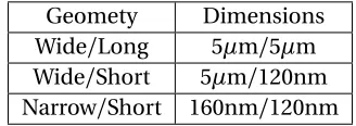
Narrow/Short geometry exhibits both Narrow and Short Channel Effects. This is the critical or worst case, as far as CMOS modeling is concerned. The following table explains notation used
for dimensions specific to this process: Table 4.1 is obtained from design kit documentation of
Geomety Dimensions Wide/Long 5µm/5µm Wide/Short 5µm/120nm Narrow/Short 160nm/120nm
Table 4.1Process Specific Dimensions
technology. From table 4.1, Narrow/Long geometry is excluded. In my understanding, devices of
Narrow/Long geometries are typically used for fabricating on-chip passive components such as resistors and capacitors. As long as these devices exhibit expected resistance or capacitance, their
region of operation can be ignored.
4.1.2 Region Specific Modeling
Two-Terminal MOS structure has been subjected to extensive research, as it was observed that de-tailed analysis of this structure unveiled few anomalies in modern technologies. By varying external
contact potentials, channel charge density can be altered in an useful way. Based on charge density
4.2. IMPLEMENTATION OF LEARNING ALGORITHM CHAPTER 4. EXPERIMENTATION
channel region, forbidding charge transfer between drain and source region. In depletion mode, channel region is devoid of any mobile carriers.
The mode of interest for most of the design engineers is Inversion, where level of conduction
can be controlled by external contact potentials. In strong inversion, channel charge density is as high as majority carrier density in substrate. Drain current is prominently contributed by Drift
Mechanism. A MOSFET in strong inversion region can be modeled as current source in parallel
with resistor in its simplest approximation. The behavior ofID with respect toVD S is strongly linear. Moderate Inversion Region represents transition between Strong Inversion and Weak Inversion. In
this region, current generation mechanism is a combination of drift and diffusion, while neither
effect in dominance.IDbehavior with respect toVD S can be considered linear. Conduction in Weak Inversion is one of the classical attributes of Short Channel Devices. Even though channel formation
near surface is meager, due to high lateral field (caused byVD S), transistors conduct even when gate
voltage is less than its threshold voltage. In weak inversion region, exponential relationship between
ID andVD Sis observed[21].
With the proliferation of hand-held electronic equipments, circuit designers are required to
consider sub-threshold operation (Weak Inversion) for improving battery life. Strong Inversion suffers from high power consumption while Weak Inversion compromises Signal-to-Noise ratio.
A fair compromise between these two conflicting demands is observed in near-threshold region (Moderate Inversion).
Gate Characteristics are variations inIDobserved by varyingVG S, whileVD S is held constant. As
VG Sis varied, transistor traverses from weak to moderate to strong inversion regions. In order to
extract information from Gate Characteristics, complex hypotheses functions are required, whose
implementation was could not be successfully done under the deadlines.
4.2
Implementation of Learning Algorithm
MATLAB®provides number of options for implementing linear and non-linear regression algorithms.
Statistics and Machine Learning Toolbox provides built-in functions that can implement various
supervised learning algorithms such as regression, support vector machines, decision trees, etc. The reader is referred to MATLAB documentation for Statistics and Machine Learning Toolbox[13].
Test data comprise of saturation region responses for weak, moderate and strong inversion and for all three geometries, mentioned in 4.1. One of the simplest approximations for modeling
saturation region is a current source in parallel with a resistor. Since the relationship in saturation
4.2. IMPLEMENTATION OF LEARNING ALGORITHM CHAPTER 4. EXPERIMENTATION
slope-intercept form.
ID = λ1+λ2×VD S (4.1)
In equation 4.1,λ1can be considered as initial current at onset of saturation. Hence, unit ofλ1is
Amperes(A). Similarly,λ2can be related to drain transconductance, with unit Amperes/Volts (A/V). Litovski et. al[11]have proposed neural network based approach for CMOS model development.
Equation 4.2 represents effective neuron transfer function. A key advantage of using exponential
model equation is it’s higher order derivatives. As stated in section 2.1.2, model equations are required to have continuous derivatives.
ID =
λ3
e(−λ4×VD S) (4.2)
In equation 4.2,λ3can be thought of as initial current (similar toλ1), and hence it has units of Amperes (A). Parameterλ4, in combination withVD Sdetermine rate of change (increase or decrease)
of drain current. From equation 4.2, it can be deduced thatλ4has units of (1/V).
The above two functions have been used as hypotheses. With each set of characteristics, values ofλ1toλ4are calculated. These values, along with their respective equations are used to reconstruct
drain characteristics. Root Mean Squared Error between test data and reconstructed characteristics
is calculated. This indicates how accurately each hypothesis function can extract parameters. It is important to make readers aware that lambda parametersλ1toλ4are not to be confused
with Channel Length Modulation parameterλC L M. However, we can prove relationship inλ1,λ2
andλC L M as follows:
ID =
β
2 ×(VG S−VT H) 2
×(1+λC L M.VD S) (4.3)
After expanding equation 4.3 and comparing it with equation 4.1, following analogy can be
deducted:
λ1 = β
2 ×(VG S−VT H)
2 (4.4)
λ2 = β
2 ×(VG S−VT H) 2×λ
4.2. IMPLEMENTATION OF LEARNING ALGORITHM CHAPTER 4. EXPERIMENTATION
From equations 4.4 and 4.5, it can be inferred thatλC L Mcan be expressed as ratio ofλ2andλ1.
λC L M =
λ2
λ1 (4.6)
This relationship can be verified by checking units ofλ1(A),λ2(A/V) andλC L M (1/V).
λ1andλ3depend on device transconductance (β), gate to source voltage (VG S), threshold voltage (VT H), in simplest approximation.λ2depends onλ1andλC L M.λC L M is inversely proportional to
the length of the device.λ4mainly represents channel length modulation component of equation
4.2, thus it also relates inversely to device length.
By definition, drain transconductance is defined as the partial derivative of drain current with
respect to drain-source voltage, while gate voltage remains constant.
gd s=
∂ID
∂VD S|VG S=C o n s t a n t
. (4.7)
By differentiating equation 4.1, drain transconductance equation for linear model is obtained as follows:
gd s−l i n=λ2 (4.8)
Similarly, for exponential model, drain transconductance is given as:
gd s−e x p =
λ3×λ4
4.2. IMPLEMENTATION OF LEARNING ALGORITHM CHAPTER 4. EXPERIMENTATION
4.3. VALIDATION CHAPTER 4. EXPERIMENTATION
4.3
Validation
Using equations 4.1 and 4.2, parametersλ1toλ4are extracted from training data. These parameters
are then substituted in equations 4.8 and 4.9 to estimate case-specific drain transconductance.
gd s results obtained by BSIM4 Spectre®models are compared with those obtained by equations
4.8 and 4.9, by calculating Root Mean Squared Error (RMSE).
R M S E =
v u u t
1
n×
n
X
j=1
(yj−yˆj)2 (4.10)
RMSE is a quadratic scoring rule that measures average magnitude of the error. RMSE between
two data sets is calculated by squaring element-wise differences, calculating mean and lastly, taking
CHAPTER
5
RESULTS
Both chosen hypothesis functions have two parameters which are modified on-the-fly, based on training data. However, two parameters can-not capture multitude of effects which take place during
normal CMOS operation. Supervised learning algorithm tries to adapt these two parameters to its
best capacity. Therefore, when gate characteristics are used as training data, these functions fail to replicate gate characteristics with required RMSE accuracy. It suffers from same misfortune while
dealing with drain characteristics as training data. These simplistic functions can replicate only a
small subset of drain characteristics (saturation region).
This chapter shows graphical comparison between training data and data generated by tuning
the hypothesis function. Importantly, first derivative (transconductance) is also compared. Gate
voltage is adjusted so as to force transistor into weak, moderate and strong inversion. Findings for each inversion region are tabulated.
In order to provide readers with general idea of accuracy, percentage errors are expressed for
5.1. STRONG INVERSION REGION MODELING CHAPTER 5. RESULTS
5.1
Strong Inversion Region Modeling
Current in Strong Inversion is prominently contributed by Drift Mechanism. Strong Inversion region
can be modeled as current source in parallel with resistor in its simplest approximation. The behavior ofID with respect toVD Sis strongly linear.
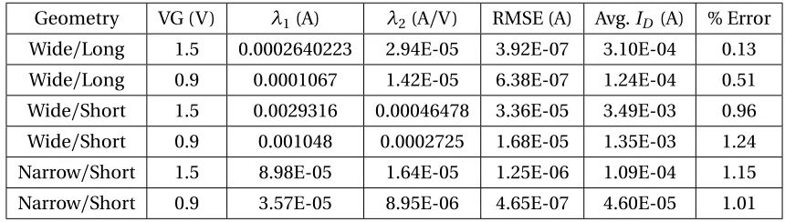
Tables 5.1 and 5.2 refer to the extracted lambda parameters obtained for transistor specific
geometry. These parameters are obtained from supervised machine learning algorithm, using saturation region drain characteristics as training data. Tables 5.1 and 5.2 also refer to the RMSE
error between reference (training) data and data produced using linear and exponential hypothesis
functions respectively. Table 5.3 is based on parameters obtained in tables 5.1 and 5.2. It evaluates fit between first derivatives of training data and replicated data.
Figures 5.1, 5.2 and 5.3 show comparison of saturation region drain characteristics, when chosen
geometries are operated in strong inversion. Figures 5.4, 5.5 and 5.6 depict graphical comparison of first derivatives.
Geometry VG (V) λ1(A) λ2(A/V) RMSE (A) Avg.ID(A) % Error
Wide/Long 1.5 0.0002640223 2.94E-05 3.92E-07 3.10E-04 0.13
Wide/Long 0.9 0.0001067 1.42E-05 6.38E-07 1.24E-04 0.51
Wide/Short 1.5 0.0029316 0.00046478 3.36E-05 3.49E-03 0.96
Wide/Short 0.9 0.001048 0.0002725 1.68E-05 1.35E-03 1.24
Narrow/Short 1.5 8.98E-05 1.64E-05 1.25E-06 1.09E-04 1.15
Narrow/Short 0.9 3.57E-05 8.95E-06 4.65E-07 4.60E-05 1.01
5.1. STRONG INVERSION REGION MODELING CHAPTER 5. RESULTS
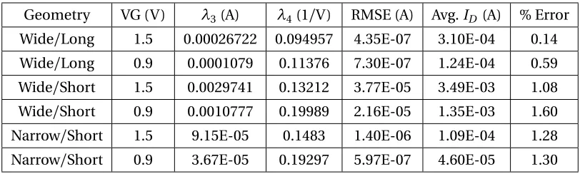
Geometry VG (V) λ3(A) λ4(1/V) RMSE (A) Avg.ID(A) % Error
Wide/Long 1.5 0.00026722 0.094957 4.35E-07 3.10E-04 0.14
Wide/Long 0.9 0.0001079 0.11376 7.30E-07 1.24E-04 0.59
Wide/Short 1.5 0.0029741 0.13212 3.77E-05 3.49E-03 1.08
Wide/Short 0.9 0.0010777 0.19989 2.16E-05 1.35E-03 1.60
Narrow/Short 1.5 9.15E-05 0.1483 1.40E-06 1.09E-04 1.28
Narrow/Short 0.9 3.67E-05 0.19297 5.97E-07 4.60E-05 1.30
Table 5.2Exponential Hypothesis Function in Strong Inversion
Geometry VG GD S (Avg.) R M S EL I N Linear R M S EE X P Exponential
(V) (A/V) (A/V) % Error (A/V) % Error
Wide/Long 1.5 3.02E-05 5.51E-06 18.25 5.97E-06 19.76
Wide/Long 0.9 1.49E-05 5.09E-06 34.13 5.61E-06 37.59
Wide/Short 1.5 5.28E-04 2.42E-04 45.86 2.64E-04 49.95
Wide/Short 0.9 3.04E-04 1.11E-04 36.65 1.33E-04 43.70
Narrow/Short 1.5 1.90E-05 9.66E-06 50.78 1.05E-05 55.16
Narrow/Short 0.9 9.83E-06 3.03E-06 30.78 3.68E-06 37.43
5.1. STRONG INVERSION REGION MODELING CHAPTER 5. RESULTS
5.1. STRONG INVERSION REGION MODELING CHAPTER 5. RESULTS
5.1. STRONG INVERSION REGION MODELING CHAPTER 5. RESULTS
5.1. STRONG INVERSION REGION MODELING CHAPTER 5. RESULTS
5.1. STRONG INVERSION REGION MODELING CHAPTER 5. RESULTS
5.1. STRONG INVERSION REGION MODELING CHAPTER 5. RESULTS
Figure 5.6NMOS Narrow/Short Drain Transconductance in Strong Inversion
From tables 5.1 and 5.2, it can be observed that for saturation region characteristics in strong
inversion, percentage error is negligible. It can also be stated that linear hypothesis functions resulted
in lower percentage error when compared point-to-point with exponential hypothesis function. Similar trend is exhibited in table 5.3 where percentage error resulted from exponential
hypoth-esis function is more than it’s linear counterpart, when compared point-to-point. However, values
5.2. MODERATE INVERSION MODELING CHAPTER 5. RESULTS
5.2
Moderate Inversion Modeling
Moderate Inversion Region represents transition between Strong Inversion and Weak Inversion. In
this region, current generation mechanism is a combination of drift and diffusion, while neither effect in dominance.ID behavior with respect toVD Scan be considered linear.
To operate a transistor in moderate inversion, it’s gate terminal must be biased at a voltage which
approximately equals to its native threshold voltage. Information about native threshold voltages of chosen geometries can be found out from technology design kit documentation.
Tables 5.4 and 5.4 refer to the extracted lambda parameters obtained for transistor specific
geometry. These parameters are obtained from supervised machine learning algorithm, using saturation region drain characteristics as training data. These tables also present RMSE error between
reference (training) data and data produced using linear and exponential hypothesis functions. Table
5.6 is based on parameters obtained in tables 5.4 and 5.5. It evaluates fit between first derivatives of training data and replicated data.
Figures 5.7, 5.8 and 5.9 show comparison of saturation region drain characteristics, when cho-sen geometries are operated in moderate inversion. Figures 5.10, 5.11 and 5.12 depict graphical
comparison of first derivatives.
Geometry VG (V) λ1(A) λ2(A/V) RMSE (A) Avg.ID (A) % Error
Wide/Long 0.1208 7.30E-08 7.10E-08 7.28E-10 1.40E-07 0.52
Wide/Short 0.4371 9.09E-06 5.33E-05 2.34E-06 6.24E-05 3.75
Narrow/Short 0.365 1.63E-07 1.40E-06 5.88E-08 1.63E-06 3.61
Table 5.4Linear Hypothesis Function in Moderate Inversion
Geometry VG (V) λ3(A) λ4(1/V) RMSE (A) Avg.ID (A) % Error
Wide/Long 0.1208 8.49E-08 0.49646 5.19E-09 1.40E-07 3.70
Wide/Short 0.4371 2.46E-05 0.84958 2.80E-06 6.24E-05 4.49
Narrow/Short 0.365 6.16E-07 0.85512 6.17E-08 1.63E-06 3.79
5.2. MODERATE INVERSION MODELING CHAPTER 5. RESULTS
Geometry VG GD S (Avg.) R M S EL I N Linear R M S EE X P Exponential
(V) (A/V) (A/V) % Error (A/V) % Error
Wide/Long 0.1208 7.11E-08 4.37E-09 6.14 2.19E-08 30.75
Wide/Short 0.4371 5.43E-05 1.01E-05 18.62 1.20E-05 22.07
Narrow/Short 0.365 1.42E-06 2.72E-07 19.22 2.79E-07 19.65
Table 5.6Drain Transconductance RMSE Comparison of Hypotheses Functions - Moderate Inversion
5.2. MODERATE INVERSION MODELING CHAPTER 5. RESULTS
5.2. MODERATE INVERSION MODELING CHAPTER 5. RESULTS
Figure 5.9NMOS Narrow/Short Drain Characteristics in Moderate Inversion
5.2. MODERATE INVERSION MODELING CHAPTER 5. RESULTS
Figure 5.11NMOS Wide/Short Drain Transconductance in Moderate Inversion
5.2. MODERATE INVERSION MODELING CHAPTER 5. RESULTS
From tables 5.4 and 5.5, it can be observed that for saturation region characteristics in moderate inversion, percentage error is negligible. It can also be stated that linear hypothesis functions resulted
in lower percentage error when compared point-to-point with exponential hypothesis function.
Similar trend is exhibited in table 5.6 where percentage error resulted from exponential hypoth-esis function is more than it’s linear counterpart, when compared point-to-point. However, some
5.3. WEAK INVERSION REGION MODELING CHAPTER 5. RESULTS
5.3
Weak Inversion Region Modeling
Conduction in Weak Inversion is one of the classical attributes of Short Channel Devices. Even
though channel formation near surface is meager, due to high lateral field (caused byVD S), tran-sistors conduct even when gate voltage is less than its threshold voltage. In weak inversion region,
exponential relationship betweenIDandVD S is observed.
Tables 5.7 and 5.8 refer to extracted lambda parameters obtained for transistor specific geometry. These parameters are obtained from supervised machine learning algorithm, using saturation
region drain characteristics as training data. These tables also present RMSE error between reference
(training) data and data produced using linear and exponential hypothesis functions. Table 5.9 is based on parameters obtained in tables 5.7 and 5.8. It evaluates fit between first derivatives of
training data and replicated data.
Figures 5.13, 5.14 and 5.15 show comparison of saturation region drain characteristics, when chosen geometries are operated in weak inversion. Figures 5.16, 5.17 and 5.18 depict graphical
comparison of first derivatives.
Geometry VG (V) λ1(A) λ2(A/V) RMSE (A) Avg.ID (A) % Error
Wide/Long 0.1 3.77E-08 3.86E-08 3.77E-10 7.44E-08 0.51
Wide/Short 0.3 -4.20E-07 3.80E-06 3.62E-07 3.38E-06 10.71
Narrow/Short 0.3 -4.15E-08 4.69E-07 3.22E-08 4.51E-07 31.93
Table 5.7Linear Hypothesis Function in Weak Inversion
Geometry VG (V) λ3(A) λ4(1/V) RMSE (A) Avg.ID (A) % Error
Wide/Long 0.1 4.43E-08 0.50903 2.86E-09 7.44E-08 3.85
Wide/Short 0.3 9.19E-07 1.1527 1.33E-07 3.38E-06 3.93
Narrow/Short 0.3 1.33E-07 1.0536 1.66E-08 4.51E-07 3.68
5.3. WEAK INVERSION REGION MODELING CHAPTER 5. RESULTS
Geometry VG GD S (Avg.) R M S EL I N Linear R M S EE X P Exponential
(V) (A/V) (A/V) % Error (A/V) % Error
Wide/Long 0.1 3.85E-08 2.14E-09 5.56 1.19E-08 30.93
Wide/Short 0.3 3.91E-06 1.58E-06 40.26 5.96E-07 15.23
Narrow/Short 0.3 4.78E-07 1.53E-07 31.93 7.73E-08 16.19
Table 5.9Drain Transconductance RMSE Comparison of Hypotheses Functions - Weak Inversion
5.3. WEAK INVERSION REGION MODELING CHAPTER 5. RESULTS
5.3. WEAK INVERSION REGION MODELING CHAPTER 5. RESULTS
5.3. WEAK INVERSION REGION MODELING CHAPTER 5. RESULTS
5.3. WEAK INVERSION REGION MODELING CHAPTER 5. RESULTS
5.3. WEAK INVERSION REGION MODELING CHAPTER 5. RESULTS
Figure 5.18NMOS Narrow/Short Drain Transconductance in Weak Inversion
From tables 5.7 and 5.8, it can be observed that for saturation region characteristics in weak
inversion, percentage error for both hypotheses functions for Wide/Long geometry is negligible. For
Wide/Long transistor, linear function still yields smaller percentage error as compared to exponential function. However, for short channel transistors (Wide/Short and Narrow/Short), linear hypothesis
function results in more than 10% error. However, exponential function yields less than 4% error in
both of these cases.
Similar trend is exhibited in table 5.9, where for Wide/Long geometry, transconductance
ob-tained by linear hypothesis function results in smaller error as compared to its exponential
5.4. INTERPRETATION OF RESULTS CHAPTER 5. RESULTS
5.4
Interpretation Of Results
It is observed that both Linear and Exponential hypothesis functions are capable of replicating
satu-ration region subset of drain characteristics (IV curves) in all inversion regions. However, percentage error numbers obtained for transconductance calculations are substandard. For example, from
table 5.3, percentage error is as high as 55.16%.
Figures depicting transconductance comparison of BSIM model and chosen hypotheses func-tions exhibit substantial disagreement for various gate voltage and drain voltage combinafunc-tions.
For example, from figure 5.5, for Wide/Long geometry biased atVD S =0.8V, it can be seen that
transconductance obtained from BSIM model is approximately 800E-06 A/V and that from linear and exponential hypotheses functions is approximately 400E-06 A/V.
The significance of percentage error in drain transconductance calculation can be illustrated by
considering an example of single stage amplifier design. Intrinsic gain of the amplifier is given as:
G a i n= gm gd s
(5.1)
Thus, any percentage error in transconductance calculations will get translated to deviation in
calculated and actual gain of the transistor. For given example, 100% error in drain transconductance will result in 100% error in gain calculation from equation 5.1.
Supervised learning algorithm breaks continuous drain characteristics for training its model. This
discontinuity, added intentionally due to limitation of hypothesis function compromises reliability of thesegd s plots. However, it asserts the fact that for development of model, continuous functions
such as exponential based functions should be used as a starting point for model development,
CHAPTER
6
CONCLUSION
As explained by Bucher et. al.[2], preliminary steps in parameter extraction procedure involve working with I-V characteristic of CMOS transistor. Machine learning methodology was expected
to replicate and predict Gate as well as Drain characteristics. However, experiments performed
exposed the inability of methodology to extract information from gate and drain characteristics. This chapter explains shortcomings of approach and reasons for failure.
6.1
Critical Analysis
6.1.1 Choice of Hypothesis Function
Gate characteristics depict transition of CMOS channel from weak inversion to strong inversion,
while passing through moderate inversion. Drain characteristics represent effect of varying lateral field for a specific channel inversion.
Chosen hypothesis functions could not replicate complete gate and drain characteristics
sat-isfactorily, as they were violating RMSE requirements. Results obtained in Chapter 5 show that hypothesis functions could replicate only a subset of drain characteristics. These equations deal
6.1. CRITICAL ANALYSIS CHAPTER 6. CONCLUSION
bulk to source voltagesVB S. This reduces four-terminal MOS device into merely two-terminal device.
This is over-simplification of MOS behavior and hence, leads to erroneous results.
As reported by Rabaey et. al.[18], a simplistic model of MOS should include at least following
key effects:
1. Threshold Voltage variations due to drain induced barrier lowering (DIBL)
2. Threshold Voltage variations due to body effect
3. Channel Length Modulation
From equations 4.1 and 4.2, it can be inferred that effects related to threshold voltage are lumped
into single parameters, namelyλ1andλ3.λ2andλ4represent channel length modulation. Since the equations did not have anyVG SorVB S terms, parametersλ1andλ3were not really "trained"
and it lead to significant errors.
Hypothesis functions with more complexity can account for these effects. Potential candidate for hypothesis function is EKV model equation[6]. (If a new model equation is to bo be developed using
this methodology, it would take continuous additions to initially chosen mathematical equation.
This will be a time consuming endeavor and there will not be any development time advantage when compared to the conventional model development flow).
6.1.2 Discontinuities
Tables 5.1, 5.3 and 5.5 summarize different values of lambda parameters extracted from partial drain characteristics. For a specific geometry, these values are different for different values of gate voltage.
This violates the key requirement of model continuity.
To obtain unique values of lambda parameters, all drain characteristics obtained for a specific geometry should be used as training data. However, due to RMSE operation performed in the
machine learning methodology, values of lambda parameters will be averaged. For instance, if drain
voltage is varied from 0V to 1.8V and drain characteristics are obtained for specific values of gate voltage such as 0V, 0.3V, 0.6V, 0.9V, 1.2V, 1.5V and 1.8V, then values of lambda parameters will be
averaged around values of lambda parameters obtained for 0.9V (central condition). This will lead
to higher RMSE values for smallest and largest gate voltage values and error will decrease as gate voltage approaches center value of 0.9V. Smaller and larger values of gate voltage are likely to violate
target accuracy metric.
![Figure 2.1 Classification of Semiconductor Device Models [21]](https://thumb-us.123doks.com/thumbv2/123dok_us/1732927.1221406/16.612.124.506.115.383/figure-classication-of-semiconductor-device-models.webp)