Available online:
https://edupediapublications.org/journals/index.php/IJR/
P a g e | 840Techniques for Reducing Power in Multipliers
P.Rajani
& Dr.G.VMahalakshmi
Department of ECE, Sreenidhi Institute of Science and Technology Hyderabad, Telangana, India
Abstract—Inthis work, another topology was proposed to advance the power scattering of Multipliers. Low power computerized Multiplier Design in view of bypassing strategy mostly used to lessen the exchanging power scattering. While this strategy offers incredible dynamic power investment funds mostly in exhibit multipliers, because of their consistent interconnection plot, it misses the lessened region and fast favorable circumstances of tree multipliers. In this way, blended style design, utilizing a customary tree based part, consolidated with a sidestep, cluster based part, is proposed. Evaluating the execution of these Multiplier structures utilizing Xilinx ISE device suite, it has been discovered that while the sidestep procedure offers the base dynamic power utilization, the blended design offers a delay*power item change , contrasted with every single other engineering.
I. INTRODUCTION
As the size of coordination continues developing, increasingly advanced flag handling frameworks are being actualized on a VLSI chip. These flag handling applications request incredible calculation limit as well as expend significant measures of vitality. While execution and zone stay to be two noteworthy plan objectives, control utilization has turned into a basic worry in the present VLSI framework outline. The requirement for low-control VLSI frameworks emerges from two principle powers. To begin with, the enduring development of working recurrence and preparing limit per chip, extensive current must be conveyed and the Warmth because of substantial power utilization must be expelled by legitimate cooling systems. Second, battery life in compact electronic gadgets is restricted.
Low power issues have turned into an essential factor in present day VLSI plan. The constrained power limit frameworks had offered ascend to more power mindful outlines by fashioners. Presently a-days, control has turned into a vital factor than territory or speed. Be that as it may, distinctive usage advancements introduce diverse power improvement openings. In advancements over 0.1um,dynamic power is the predominant commitment to the aggregate power scattered while in littler innovations;
spillage control is increasing more significance. Dynamic power dispersal is the aftereffect of charging the heap capacitances in a circuit. It is given by condition
𝑃𝑑𝑦𝑛𝑎𝑚𝑖𝑐= 𝐶𝐿𝑉𝐷𝐷2 E(sw)𝑓𝑐𝑙𝑘
Where, 𝐶𝐿 is the yield capacitance, the supply
𝑉𝐷𝐷 voltage, E(sw) (called exchanging action) is the normal number of changes and the clock recurrence𝑓𝑐𝑙𝑘.
There are two primary decisions for the plan of a multiplier. The first is the Wallace tree frame, which has the upside of a logarithmic circuit delay, and the second is the exhibit multiplier shape, similar to the Carry-Save cluster, where the deferral is direct. Then again the exhibit multiplier has a standard structure, which prompts a thick format making it perfect for creation.
The Wallace tree has unpredictable structure, possesses more territory on the wafer, and requirements more noteworthy wiring for cell interconnections. This point is significant for present and rising IC advances, where interconnection assumes a dominating part. This factor influences the Wallace to tree improper for low power applications. In this paper, we introduce a strategy to limit control dispersal in computerized multipliers, beginning from dynamic power and focusing on the exchanging movement. There have been proposed a ton of methods to diminish the exchanging action of a rationale circuit. In the consecutive world a standout amongst the best is clock gating, where an empower flag hinders the clock, disconnecting a huge square of the circuit. This system disposes of movement and in this manner, control utilization.
Available online:
https://edupediapublications.org/journals/index.php/IJR/
P a g e | 841with different isolating components have also been reported in the past, in. However, our contribution moves one step further and proposes a mixed architecture, to address both dynamic power dissipation and performance, by doing half of the multiplication through an array structure, with bypass transmission gates, and the other half through a Wallace tree. This mixed architecture offers a delay*power product improvement ranging from 1.2x to 6.5x, compared to all other architectures.
Minimization of the switching activity in a digital circuit can be performed by isolating and blocking units producing non-valuable partial results, in order to save power. To perform isolation, transmission gates can be used, as ideal switches with small power consumption, propagation delay similar to the inverter, and small area. Isolation by transmission gates can be applied to any kind of logic circuit. However in this paper we are considering digital multipliers, starting with the canonical and widely used Carry-Save array topology.
II. LITERATURE SURVEY
Digital Signal Processing (DSP) regularly includes increases with an arrangement of coefficients. S. Kim, S. Hong, M. Papaefthymiou, and W. E.Stark exhibited a novel multiplier outline system for playing out these coefficient duplications with low power scattering. Given limits on the throughput and the quantization blunder, our approach scales the first coefficients to empower the apportioning of every increase into a gathering of littler augmentations with shorter basic ways. Huge vitality investment funds are accomplished by playing out these duplications in parallel with a scaled supply voltage. Dispersal is additionally lessened by incapacitating the multiplier pushes that don't influence the duplication's result. We have utilized our procedure to plan a low-control parallel multiplier for the Fast Fourier Transform.
Reproduction comes about demonstrate that
ourapproach can bring about critical power reserve funds over regular multipliers.
P. Meier, R. A. Rutenbar, and L. R. Carley displayed Multiplication a principal building hinder in all DSP errands. Because of the expansive inertness inalienable in duplication, plans have been contrived to limit the deferral. Two techniques are basic in current usage: standard clusters and Wallace trees. Past door level examinations have proposed that not exclusively are Wallace trees quicker than cluster plans, they additionally devour significantly less power. However these investigations did not consider, bringing about idealistic planning and power gauges. We build up a disentangled relative format strategy to examine the impact of physical design on these outlines.
III. BASIC ARCHITECTURES A. Carry Save Array Multiplier:
The Carry-Save cluster multiplier is a direct usage of vector duplication. It is favored in a few executions in light of its sanctioned interconnect topology. It comprises of a fractional item lessening tree, which is utilized to compute halfway items in Carry-Save excess frame, and a last fasten snake to change the repetitive shape in typical parallel shape. A 4x4 Carry-Save multiplier is appeared in figure1.
The functionality of the Carry-Save array
multiplier is as follows: We assume that 𝑋 =
(𝑥𝑛−1, … … 𝑥1𝑥0) and𝑌 = (𝑦𝑛−1, … … 𝑦1𝑦0) are unsigned numbers.
Figure1. A 4x4 carry save multiplier
The bits are fed into an array of FA* cells shown below figure2(a).
Available online:
https://edupediapublications.org/journals/index.php/IJR/
P a g e | 842Figure2(b).FAB Cell
Each FA* cell performs the multiplication 𝑥𝑖× 𝑦𝑗using an AND gate and then adds the result with
the incoming carry bits, to produce an output sum and an output carry. All FA* cells are appropriately connected (sums and carries) as shown in figure 1, to perform the multiplication. The final adder shown in figure 1 is used to merge the sums and carries from the last row of the array, since in every row the carry bits are not immediately added but rather propagated to the row below. We can see that when 𝑦𝑗 is 0 then the
corresponding diagonal cells are functioning
unnecessarily. In all these cells the partial products𝑥𝑖×
𝑦𝑗 and the carry inputs are zero for
𝑡 = 0,1, … … , 𝑛 − 1 and this chain does not contribute to the formation of the product. Consequently, the sum output of the above cell can bypass this unimportant diagonal with the use of transmission gates. To achieve all of the above we can replace the FA* cell with the cell in figure shown above (called the FAB cell).
B.CSA with Bypassing Technique:
The transmission gates in the FAB cell lock the inputs of the full adder to prevent any transitions. When y = 0 , and a multiplexer propagates the sum input to the sum output. When y = 1 , the sum output of the full adder is passed. The carry input does not generate any new value since the initial diagonal carry input is always 0. So, no transmission gate is used to block it. If y = 0 , to fix any erroneous carry generated from previous computations, an AND gate is used before the final adder to make the final diagonal carry output 0. The whole structure of the modified multiplier is presented in figure 3.Consequently, the sum output of the above cell can bypass this unimportant diagonal with the use of transmission gates.
Figure3. 4 x 4 Carry Save Array Multiplier with Bypass
C.Wallace Tree Multiplier:
Wallace tree is an efficient hardware implementation of a digital circuit that multiplies two integers.
Figure4.Wallace Tree
The Wallace tree has three steps:
1. Multiply (that is - AND) each bit of one of the arguments, by each bit of the other, yielding 𝒏𝟐 results.
2. Lessen the quantity of incomplete items to two by layers of full and half adders.
3. Gathering the wires in two numbers, and includes them with a regular adder.
The second stage fills in as takes after. For whatever length of time that there are at least three wires with a similar weight include a following layer:
• Take any three wires with similar weights and
Available online:
https://edupediapublications.org/journals/index.php/IJR/
P a g e | 843• If there is only one wire left, interface it to the following layer.
The advantage of the Wallace tree is that there are as it were𝑶(𝒍𝒐𝒈𝒏) reduction layers, and each layer has 𝑂(1)propagation delay. As making the partial products is 𝑂(1)and the final addition is 𝑂(𝑙𝑜𝑔𝑛), the multiplication is only 𝑂(𝑙𝑜𝑔𝑛), not much slower than addition (however, much more expensive in the gate count). Naively adding partial products with regular adders would require 𝑂(𝑙𝑜𝑔2𝑛)time.
D.Mixed Architecture:
The mixed architecture is nothing but the combination of Wallace tree and Array structure. The great timing advantage of the Wallace tree along with the great power advantage of the bypass scheme can be combined in a mixed architecture. The figure for mixed architecture is shown in figure 5.
In general, array multipliers offers dynamic power saving but it fails to give a reduced area and fast
speed advantages because of their regular
interconnection pattern. So, tree multipliers are introduced to achieve reduced area and fast speed, to achieve both delay and power advantages it is better to use a different architecture that is having two parts one is tree based part and other is bypass architecture. The modified bypass technique offers minimum dynamic power compared to normal carry save array multiplier. The tree based part of the mixed architecture has enough timing slack to be implemented using high threshold voltage components. Two 8 bit values can be multiplied by splitting each one of them in two 4 bit parts.
Figure5. A 16 bit multiplication split in parts
If the first 8 bit value is (A,B) and the second is (C,D), four 8 bit products are generated,
𝑋 = 𝐴 × 𝐷,𝑌 = 𝐵 × 𝐷,𝑍 = 𝐴 × 𝐶 and 𝑊 = 𝐵 × 𝐶 . These four partial products shifted and added together generate the final 16 bit multiplication. The key point behind operand splitting is to use different multiplier
example of figure shown above𝑋 = 𝐴 ×, and 𝑍 = 𝐴 × 𝐶 are performed in Wallace multipliers while the others in a bypass architecture. So, from 𝑋 = 𝐴 × 𝐷and𝑍 = 𝐴 × 𝐶 performance is gained while from 𝑌 = 𝐵 × 𝐷 and 𝑊 = 𝐵 × 𝐶 power is gained. If half of one or both operands usually contain more 0s than 1s, this specific half should be passed through the bypass multiplier for greater power improvements. For example, the architecture of figure shown above gives better results when contains on average more 0s than 1s.
EXTENSION: Vedic Architecture:
The equipment engineering of 4x4 piece Vedic multiplier (VM) modules are shown in the underneath areas. Here, "Urdhva-Tiryakbhyam" (Vertically and Crosswise) sutra is utilized to propose such a design for the increase of two double numbers. The excellence of Vedic multiplier is that here incomplete item era and increases are done simultaneously. Henceforth, it is very much adjusted to parallel preparing. The element makes it more appealing for paired augmentations. This thusly decreases delay.
Vedic Multiplier for 4x4 bit:
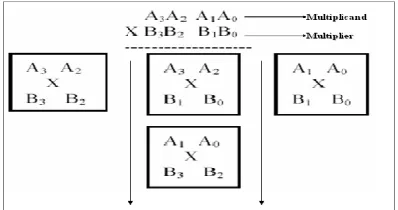
Separation the no. of bits in the data sources similarly in two sections. We should break down 4x4 piece augmentation, say multiplicand A=A3A2A1A0 and multiplier B= B3B2B1B0. Following are the yield line for the duplication result, S7S6S5S4S3S2S1S0. How about we isolate An and B into two sections, say "A3 A2" and "A1 A0" for An and "B3 B2" and "B1B0" for B. Utilizing the principal of Vedic increase, taking no-account at once and utilizing 2 bit multiplier piece, we can have the accompanying structure for 4x4 piece augmentation as appeared in Figure6.
Available online:
https://edupediapublications.org/journals/index.php/IJR/
P a g e | 844Each square as appeared above is 2x2 piece multiplier. Initial 2x2 multiplier inputs are "A1 A0" and "B1 B0". The last square is 2x2 piece multiplier with inputs "A3 A2" and "B3 B2". The center one shows two, 2x2 piece multiplier with inputs "A3A2" and "B1B0" and "A1A0" and "B3B2".
So the last aftereffect of duplication, which is of 8 bit, "S7S6S5S4S3S2S1S0". To comprehend the idea, the square graph of 4x4 piece Vedic multiplier is
appeared in Figure7. To get last
itemS7S6S5S4S3S2S1S0 four, 2-bit Vedic multiplier and three 4-bit Ripple Carry (RC) Adders are required. In this proposition, the initial 4-bit RC Adder is utilized to include two 4-bit operands got from cross increase of the two center 2x2 piece multiplier modules. The second 4-bit RC Adder is utilized to include two 4-bit operands, i.e. linked 4-bit ("00" and most critical two yield bits of right hand the vast majority of 2x2 multiplier module as appeared in Figure 7) and one 4-bit operand we get as the yield aggregate of first RC Adder. Its convey "ca1" is sent to third RC Adder. Presently the third 4-bit RC Adder is utilized to include two 4-bit operands, 3i.e. connected 4 - bit (convey ca1, "0" and most critical two yield aggregate bits of 2 ndRC Adder as appeared in Figure 8) and one 4-bit operand we get as the yield whole of left hand a large portion of 2x2 multiplier module. Early writing talks about Vedic multipliers in light of cluster multiplier structures. The course of action of Ripple Carry Adder as appeared in Figure 8 causes us to diminish delay.
Figure 7: Block Diagram of 4x4 bit Vedic Multiplier (VM)
Figure 8: Circuit Diagram of 4 bit Ripple Carry Adder
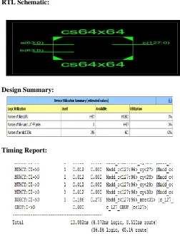
IV. SIMULATION RESULT Simulation:
RTL Schematic:
Design Summary:
Timing Report:
V. CONCLUS ION
In this work, we have implemented Multipliers for Low power Applications. For power optimization, two basic algorithms, namely Wallace Tre6e and Array Multiplier, are combined to exploit the low power and High Performance
gains from the individual architectures.Power
Available online:
https://edupediapublications.org/journals/index.php/IJR/
P a g e | 845VI. REFERENCES
1) DimitrisBekiaris, George Economakos and
KiamalPekmestzi, "A Mixed Style Multiplier Architecture for Low Dynamic and Leakage Power Dissipation," in International Symposium on VLSI Design Automation and Test (VLSI-DAT). IEEE, 2010, pp. 258-261
2) M. Karlsson, “A generalized carry-save adder array for digital signal processing,” in 4th Nordic Signal Processing Symposium. IEEE, 2000, pp. 287–290.
3) P. Meier, R. A. Rutenbar, and L. R. Carley, “Exploring multiplier architecture and layout for low power,” in Custom Integrated Circuits Conference. IEEE, 1996, pp. 513–516.
4) N. Weste and D. Harris, CMOS VLSI Design: A Circuits and Systems Perspective - Third Edition. Addison-Wesley, 2004.
5) C. C. Wang and G. N. Sung, “Low-power
multiplier design using a bypassing technique,” Journal of Signal Processing Systems, 2008. 6) S. Kim, S. Hong, M. Papaefthymiou, and W. E.
Stark, “Low power parallel multiplier design for
dsp applications through coefficient
optimization,” in 12th Annual International ASIC/SOC Conference. IEEE, 1999, pp. 286–290.
7) G. Economakos and K. Anagnostopoulos, “Bit
level architectural exploration technique for the design of low power multipliers,” in International Symposium on Circuits and Systems. IEEE, 2006.
8) Prakash Narchi, Siddalingesh S Kerur, Jayashree C Nidagundi, Harish M Kittur and Girish V A. Implementation of Vedic Multiplier for Digital
Signal Processing. IJCA Proceedings on
International Conference on VLSI,