processing and probe connection
Naoya Torii1,2, Dai Yamamoto1, Masahiko Takenaka1, and Tsutomu Matsumoto2
1
Secure Computing Laboratory, Fujitsu Laboratories Ltd. 2 Graduate School of Environment & Information Sciences,
Yokohama National University
Abstract. PUF (Physically Unclonable Function) technologies attract attention as a candidate to prevent counterfeit chips. A latch PUF is known as a high performance PUF among various types of proposed PUFs. In this paper we describe an experiment on a dynamic attack to a latch PUF consisting of RS latches, such as measuring the latch output by a probe connection after a FIB (Focused Ion Beam) processing. As a result, we confirmed that the latch PUF using the RS latch has a tolerance for the dynamic analysis, because the RS latch output was influenced and changed by the FIB processing in our experiment.
1
Introduction
Recently, smart cards and hardware tokens are widely used for personal au-thentications and electric payment, etc. These devices include hardware, which is thought to be secure because it is difficult to retrieve or reveal secret infor-mation stored in the nonvolatile memory. However, counterfeiting the hardware becomes possible by the development of IC reverse engineering technologies[5]. PUF (Physically Unclonable Function) technologies attract attention as a can-didate to prevent counterfeit chips [1] [2] [3] [4].
A PUF (silicon PUF) amplifies uniqueness of physical characteristics, such as drive capabilities of logic gates and wiring delay at each IC, and generates different responses based on each IC’s characteristic. On the other hand, a circuit pattern of the silicon PUF is identical between each IC. It is difficult to reveal the response using the circuit patterns, so the PUF can prevent counterfeit the chip. The PUF is an efficient countermeasure against a static attack (analyzing the PUF at the time of power-off state).
2
of the chip are necessary, but these influence physical characteristic of the PUF circuit. Therefore, reading the original output value is thought to be difficult. Actually, the output of a coating PUF [6] is influenced by some processing on the chip. However, there is no report to confirm the above-mentioned characteristic by experiments concerning other types of digital PUFs including latch PUFs.
In our experiment, at first RS latches were prototyped on test chips using 0.18um CMOS technology. Next, the output wiring of the targeted RS latch was exposed by FIB (Focused Ion Beam) processing, and we contacted a microprobe to the output wiring in order to confirm whether the output value of the RS latch was influenced. As a result, it was confirmed that some RS latch outputs were affected by the processing of the FIB. This shows the possibility that PUF using RS latch can have the tolerance for the dynamic analysis.
2
The experiment
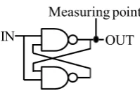
A test chip includes a latch PUF consisting of 256 RS latches. When a continuous standing up signal (= clock signals) is input to each RS latch, output values of each RS latch become either of 0s/1s/random numbers.
2.1 Chip processing by the FIB
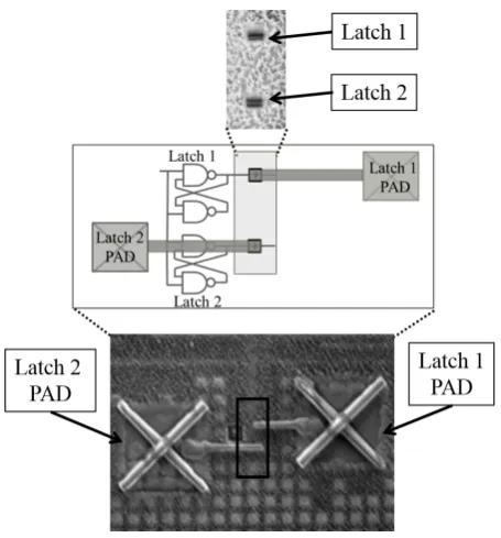
Figure 1 shows the location of measurement of the RS latch. At first the latches for FIB processing were selected by the layout data of the test chip. The locations of measurement should be no wires over them and easy to be exposed from the surface of the chip by the FIB processing. Three lathes per chip were selected out of 256 in this experiment. The output wire of the targeted RS latch on the test chip was exposed by the FIB processing, which is shown upper picture in Figure 2. The output wire can be seen as a white line in the rectangle hole by FIB processing. The block diagram in the middle of Figure 2 shows two cross-shaped PADs, each of which is connected with each exposed output wire, and its picture is shown in the bottom in Figure 2. This PAD enables us to easily read the output values of the exposed output wire by using a measurement probe. The probe is Model 12C provided from U.S. GGB Industries.
Fig. 2.Chip Picture
2.2 Measurement environment
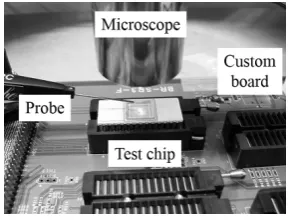
Figure 3 and Figure 4 show a measurement environment for this evaluation and its photograph, respectively.
Output data from a RS latch are transmitted to the custom and FPGA boards, and finally obtained from a user PC through RS232C cable. The FPGA board includes interface circuit, which sends some commands for data acquisition to the custom board (test chip), and also receives output data from the latch to the user PC.
In this experiment, we chose an advantageous setting for an attacker. The test chip is fabricated on relatively large 0.18 um CMOS process, so the measurement by the probe is easier than the chip using a more advanced process. Moreover, the experiment is conducted by a third-party company for fair evaluation.
The FIB system and the probe, etc. are generally used equipment installed in the contractor’s laboratory, and all layout data of the test chip is provided to the contractor for an accurate FIB processing.
3
Result of a measurement and evaluation
4
Fig. 3.Block diagram measuring environment
Fig. 4.Picture of measurement environment
the FIB processing, (B) a time when the probe is not connected to the PAD after the FIB processing, and (C) a time when the probe is connected to the PAD after the FIB processing.
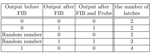
Table 1 shows the result of measurement of the latch output, the number of latches is 12 in four test chips. From this result, some latch outputs change only by the FIB processing, and the other outputs do not change. When the probe is connected to the PAD, the latch output does not change. From this result, the test chip characteristics are not stable and permanent if the test chip is modified by the FIB processing and the probe connection, so it is difficult to measure the original output value from the test chip in this experiment. Moreover, all latches are not influenced by the probe connection. The possible reason is that the latch characteristics are already biased by the FIB processing. That is, the influence by the probe connection is smaller than that of the FIB processing.
4
Conclusion
Table 1.Measurement result
Output before Output after Output after the number of
FIB FIB FIB and Probe latches
0 0 0 2
0 1 1 2
Random number 0 0 2
Random number 1 1 2
1 0 0 4
From this result, it is expected that random number generator based on latch circuits and circuits based on metastability/oscillation also have the tolerance for the dynamic analysis.
We will discuss these subjects in more detail. Moreover, we will evaluate the influence by the probe connection by the experiment.
References
1. T. Matsumoto, et al., ”Clone Resistance Based Authentication Scheme, ” In IE-ICE The 1997 Symposium on cryptography and information security, SCIS 97-19C, Jan.29 - Feb.1, 1997.(in Japanese)
2. Y. Su, J. Holleman, and B. Otis., ”A 1.6pJ/bit 96% Stable Chip-ID Generating Circuit using Process Variations,” In IEEE International Solid-State Circuits Con-ference (ISSCC 2007), pp. 406 - 407, and pp. 611, 2007.
3. Y. Su, J. Holleman, and B. Otis., ”A Digital 1.6pJ/bit Chip Identification Circuit Using Process Variations,”Solid-State Circuits, IEEE Journal of, 43(1), pp. 69-77, 2008.
4. Ravikanth S. Pappu, ”Physical One-Way Functions.,” PhD thesis, Massachusetts Institute of Technology, 2001.
5. R. Torrance and D. James., ”The State-of-the-Art in IC Reverse Engineering,” In CHES 2009, pp. 363-381. Springer, 2009.