Progress In Electromagnetics Research C, Vol. 96, 229–242, 2019
Substrate Integrated Waveguide Circular Antenna for Terahertz
Application
Radhoine Aloui*, Zied Houaneb, and Hassen Zairi
Abstract—This paper presents a multi-band annular ring antenna that is obtained from a single-layer probe-fed substrate integrated waveguide based on a graphene material, with three top plan slits. In order to create a multi-bands antenna, we conduct simulation of the antenna structure based on CST/HFSS, so we use parametric tuning to adjust TM modes. Simulations show a good results between the two methods (finite element method and integral method) CST and HFSS Simulators. The bandwidths for three modes are 340 GHz in first mode, 346 GHz in the second mode, and 104 GHz in the third mode. The simulation gains atT M11,T M02, andT M12are 8.2 dB, 8 dB, and 11 dB, respectively. The proposed antenna can be used in therahertz applications.
1. INTRODUCTION
THz applications band is a portion of optoelectronic systems, including frequencies in the range 0.3 THz to 30 THz [1]. Optical spectrum systems have received considerable attention from scientific community for generation and imagery of terahertz (THz) radiation, with numerous applications in spectroscopy, imaging, sensing, astronomy, spectroscopy, etc. [2–7]. As interest in Terahertz communication and imaging systems has increased in modern medical and satellite-related industries, it has become more challenging to obtain cutting-edge technology for payload and ground systems from other countries and has a high quality for medical imaging. In previous years, researchers have been attracted to a new technology: substrate integrated waveguide (SIW). This technology is a new technology well adapted and easy to integrate, thus improving several RF circuits. There are several passive and active RF circuits [8– 12]. Several multifunctional and multi-band antennas have been presented in the last years for some specific applications. In [13], we can find a loop-type antenna presented with dual-band omnidirectional patterns. Compact multimode patch antennas were proposed. In [14] these antennas worked at a single frequency with two different radiation modes for MIMO applications. These antennas have disadvantages of two inputs connectors, low gain, and multi-layer of substrates. The annular ring patch antenna proposed in [15] worked at multibands and multi-modes, with tuning all design parameters. However, there are few Terahertz antennas which can realize multiband and dual-mode characteristics simultaneously with a high gain for imagery application and Terahertz telecommunications. Terahertz system [16] has attracted much research and industrial attention in recent years, due to the limit of GHz band. However, the invention of graphene material is a breakthrough in the development of THz devices and applications. In [17], a graphene-based receptor has outstanding flexibility compactors properties. To stay away for congestion, the researchers prefer to use a multi-band antenna for many Terahertz applications. In this paper, a new multiband design and multi-mode antenna is presented, with high gain and wide band. The previous antenna has three bands, and each works for different modes (T M11, T M02, and T M12). In this paper, a novel graphene circular antenna with a multiband, SIW cavity
Received 6 August 2019, Accepted 27 September 2019, Scheduled 4 November 2019 * Corresponding author: Radhoine Aloui ([email protected]).
and three annular ring slots antenna is proposed, connected by a simple probe feed, and works at three different frequencies. However, the three operating frequencies can be independently tuned by adjusting the structure parameters of each ring circular antenna. Then, this paper is organized as follows. Section 2 describes the formalization of graphene material and the geometry of the antenna system. Section 3 presents the design, results, and parameters of the antenna. The parametric study, variation of the frequency-tunable method and gain are presented in Section 4. Finally, the conclusion is written in Section 6.
2. FORMULATION
2.1. Conductivity Graphene
The graphene sheet is a two-dimensional material composed of carbon atoms bonded in hexagonal structures. Its surface conductivity can be represented using the well-known Kubo formalism, and it consists of two terms, intraband conductivity and interband conductivity [24, 25]. The intraband term can be calculated as
σintra =−j e 2K
BT π2(ω−j2Γ)
⎡ ⎣ μc
KBT + 2 ln
⎛ ⎝e−
μc KBT + 1
⎞ ⎠ ⎤
⎦ (1)
and the interband conductivity is
σinter −j e 2
4πln
2|μc| −(ω−j2Γ) 2|μc|+ (ω−j2Γ)
(2)
where KB is the Boltzmann constant, the reduced Planck’s constant, e the electron charge, ω the angular frequency, Γ the scattering rate, T the temperature, and μc the chemical potential. The intraband conductivity dominates the value of total conductivity in the THz band, whereas the interband term has no significant effect on the total surface conductivity within this band. Hence, the conductivity of graphene can be expressed by using the only intraband term.
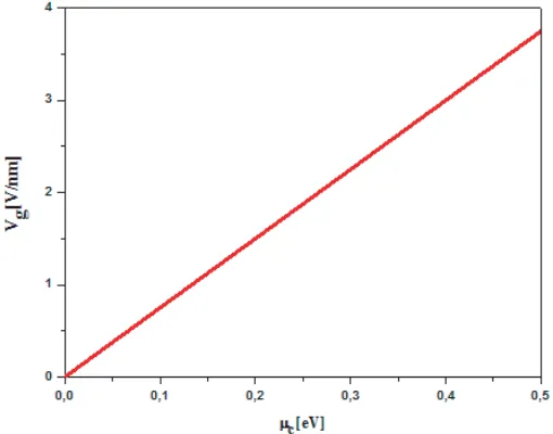
Figures 1 and 2 show the effect of changing graphene chemical potential on the real and imaginary parts of the surface conductivity. It depends on the carrier density, which can be controlled by an electric bias field. We conclude that the chemical potential increases consequential to bias voltage growth, hence the increase of the conductivity can be shown in Figure 3. The shifting of resonance frequency is due to changing.
Progress In Electromagnetics Research C, Vol. 96, 2019 231
Figure 3. The relationship between bias voltage and chemical potential.
(a) (b)
Figure 4. Comparison of the total and the intraband conductivity of the graphene sheet: (a) Real part, and (b) imaginary part.
According to Eqs. (1) and (2), the graphene material can show two types of domains. In the first step, the intraband is dominant in the frequency range from 0 to 8 THz. Elsewhere, frequency range 8 to 30 THz is a part of the interband and intraband. Figure 4 shows the shifting at frequency level between two domains. We observe that the shifting frequency is obtained from 8 THz, where interband conductivity term becomes significant.
2.2. Theoretical Analysis of Circular Antenna
Fundamental TM mode for the circular ring antenna can be demonstrated in [18]. Furthermore, the principalT M11mode is considered in this paper. Although the field distribution between ring top patch and bottom ground antenna does not vary the thickness of the patch, sincehλand the substrate is not magnetic, the resonant frequencies for different modes are determined by
fmn= KmnC
Figure 5. Design of annular antenna.
where indexmnis the order of modes,rthe dielectric value,cthe velocity if the light is in vacuum, and Kmn the eigenvalue obtained according to the boundary condition. The resonance wavelength of the TM mode is approximately equal to the average circumferential length of the ring resonance. However, it is equal to 2π (Rave), whereRave = (R1+R2)/2, andR1,R2can show the outer and inner radii of the circular ring antenna, which can be shown in Figure 5. Finally, the resonance wavelength is considered in the following expression:
λg = 2π Rave (4)
The height of the SIW circular ring antenna must be minimal compared with the wavelength λ0 in free space or the radius of the top patch. Furthermore, a cavity model can be used to synthesize the annular ring antenna for the lower TM modes. In this synthesizer, the feeding line is a connector SMA probe feed coaxial considered. Although there is a leakage current at the open edge of the circular slit in top patch antenna, the cylindrical annular cavity is considered to have a radiusReff which represents a part of the effective radius of the circular patch antenna [19] which can be calculated by
Reff =R
1 + 2h πRr
lnπR 2h
+ 1.7726 (5)
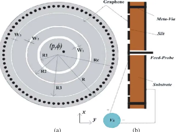
In the opportunity to excite the lowest three modes, we must show a fed probe position precisely. This parameter is the main factor to excite the three modes. Compared to the simple cavity model, the region between the one circular patch and the second ring patch is considered as a cavity electric. Figure 6 shows one circular patch and two circular rings with end final SIW cavity. The space between two short circuit regions can be considered an electric field. As indicated in the theory, the electric field can be shown in the component z-direction of arbitrary point (ρ,φ,z) in the circular patch, and a cylindrical coordinate can be written as [20, 21].
EZ=E0cosnφ[AnJn(Krρ) +BnYn(Krρ)] (6) Since the angle is equal to zero, the field expression gives a final expression:
EZ(φ=0) =E0[AnJn(Krρ) +BnYn(Krρ)] (7) whereJn (Krρ) andYn(Krρ) are the first and second species Bessel functions of order n, respectively, and Kr is the wave-number in the dielectric substrate. E0 is the constant amplitude, andAn, Bn are the coefficients and given by:
An = Y
n(KrR2)Jn(Krρ)−Jn(KrR2)Yn(Krρ)
Yn(KrR1)Jn(Krρ) +Jn(KrR1)Yn(Krρ) (8) Bn = Y
n(KrR1)Jn(Krρ)−Jn(KrR1)Yn(Krρ)
Progress In Electromagnetics Research C, Vol. 96, 2019 233
(a) (b)
Figure 6. Geometry of the proposed antenna. (a) Top view. (b) Side view. The parameters of the antenna are fixed as offset = 4µm, R = 20µm, Rs = 17.5µm, R1 = 6.5µm, R2 = 12.5µm, R3 = 15.8µm, w1= 0.5µm, w2= 0.5µm, w3= 0.2um.
Application of the SIW boundary cavity condition at (ρ=Rs3,ρ=Rs2) and (ρ=Rs2,ρ=Rs1) leads the characteristic equation for the resonance TM mode:
Jn(KrRs3)Yn(KrRs2) +Yn(KrRs3)Jn(KrRs2)
+Jn(KrRs2)Yn(KrRs1) +Yn(KrRs2)Jn(KrRs1)= 0 (10) In T M01 mode, the resonance frequency can be zero without conductive via [22, 23], so in this work, we focus on the lowest three modes of the circular antenna, T M11, T M02, and T M12. In [18], the authors show that the fundamental T M11 and T M12 modes can radiate bore sight beams and the rigorous analysis. Furthermore, T M02 mode can be used to generate a vertically polarized and conical radiation pattern [22]. In this paper, we focus on showing a Terahertz multiband multifunctional antenna, which can be selected at three bands with four patch-like and three monopolar radiation patterns for the three modes. However, in order to determine electrical parameters, the input wave port with specific boundary condition can be applied on the circular patch.
S11= Γ0
1−ej2nK0e (1−Γ2
0ej2nK0e)
(11)
where Γ0= (Zin−1)(Zin+ 1)−1, the input impedanceZin is given by
S11=±
1−S11 1 +S11
−1/2
(12)
The refractive index (n) is calculated by:
n= 1
K0e
ln(ej2nK0e+ 2mn−iln(ej2nK0e (13)
where e = maximum dimension of dielectric, m is the periodicity branch of the cosine function, and K0 is the wave number in the void. The refractive index can have two parts, the real component and complicated part. The permittivity and permeability can be calculated by the following expression, respectively:
= n
3. ANTENNA DESIGN AND RESULTS
3.1. Theoretical Analysis of Circular Antenna
At first, a circular slit with a radiusR1 and a widthW1 is cut from the top patch as shown in Figure 6. Then a second W2 is small to W1 (w2 ≤w1), which can make the coupling between the two annular rings circular. Finally, a third circular slit with a radiusR3 and a width ofW3 is tiny compared toW1 and W2 (W3 ≤ (W1, W2) and can be shown the coupling between the end annular ring and the latest annular ring with SIW.
In the first step, we redesign a conventional circular antenna into a SIW feeding version. The antenna is simulated on a single layer with a thickness of the substrate h = 1.5µm. The dielectric constant r = 2.2 and loss tangent tanδ0.0009. The antenna has an overall circular dimension of approximatelyR= 20µm. The antenna parameters are going to be changed each time to the following values R1 = 6.5µm, R2 = 12.5µm, R3= 15.8µm, andRs = 17.5µm. The obtained distances between the two rings of the annular patch are w1 = 0.5µm, w2 = 0.5µm, and w3 = 0.2µm. The antenna is excited by a coaxial probe feed which is centered along the y-axis, but offset along the x-axis by offset = 4µm to from the center of the substrate.
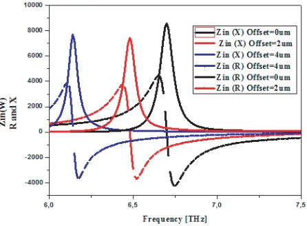
Firstly, it is observed in the simulation results of Figure 7 that the resonance (T M02 mode) can be obtained at 13.8 THz when the offset is 0. However, when the distance between the center of the antenna and the fed probe position is increased, another resonance frequency can be shown and increases for a lower mode (T M11 mode), and a higher resonance frequency (T M12 mode) appears. With offset increasing, the impedance Zinput match for T M11 and T M12 modes gets better while that for T M02 mode gets worse. Finally, we must change the offset of the fed probe for the appearance of lower three band modes (T M11,T M02, andT M12). Equation (8) shows the appearance of the other two modes, so the coaxial probe shift effect for the center of the antenna can show the excision of the second Bessel function which finally gives the last modesT M11,T M02, andT M12.
Figure 7. Reflection coefficient of the antenna with various of offset.
Figure 8. Input impedance characteristic (Imaginary and Real) with various of offset.
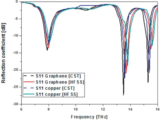
3.2. Comparative Investigation of No-Doped Graphene and Metal
Progress In Electromagnetics Research C, Vol. 96, 2019 235
Figure 9. Performance comparison of the reflection coefficient versus frequency.
(a) (b)
Figure 10. Current distribution T M11 mode. (a) Graphene. (b) Copper.
3.3. Simulation of the Tunable Antenna Based on Hybrid Metal-Graphene
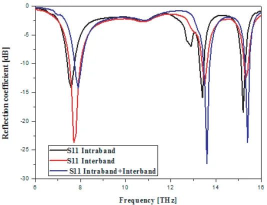
We have three resonant frequencies. The first T M11 mode is in a frequency range lower than 8 THz, and the second and third modesT M02and T M12are higher than 8 THz, respectively. We use a hybrid graphene material, intraband for the frequency lower than 8 THz, and interband for frequency more than 8 THz. On the other hand, T M02and T M12 can be simulated by intraband and interband graphene.
Figure 11. Simulation results graphene obtained for Reflection coefficient between interband, intraband and hybrid.
3.4. Results
Figure 8 shows a proper match input field probe impedance for 4µm offset. The CST simulations and HFSS software simulations show a good agreement. After optimization with this software, a right impedance and radiation performance can be achieved with the parameters fixed as those for the initial parameters.
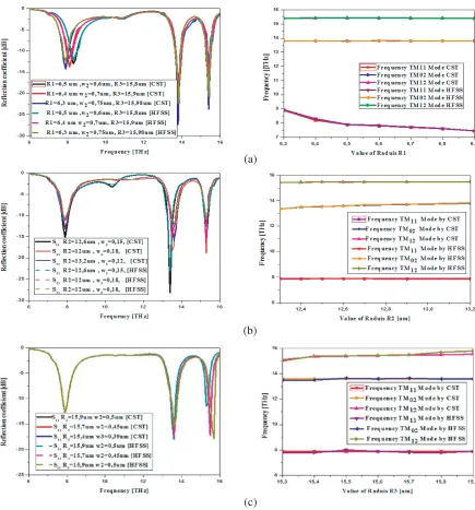
The antenna design is stimulated by HFSS software, and co-simulation by CST-studio shows different results. The simulations by the two software reflections coefficients with the value of radiusRi (i= 1,2,3) can be shown in the previous Figure 12. It is demonstrated that there is good agreement between simulations with FEM method and integral method. The bandwidth of the antenna is measured when the reflection coefficient is less than −10 dB; therefore, the bandwidths for T M11, T M02, and T M12 are respectively around 300 GHz, 300 GHz, and 100 GHz. The simulation results, presented in Figure 12, show the importance to change the resonant frequencies by the radius and slits for this antenna. Figure 12(a) shows the value of R1 parameter. It can give a change to the three modes of TM. However, Figure 12(b) shows the coefficient reflection with the value at the R2 parameter. The simulation results indicate that when the R1 parameter is invariant and R2 parameter is changed, it shows the invariant of T M11 mode, but we notice the variation at the level of the second and third modes T M02 and T M12, respectively. Finally, the third mode T M12 can be changed and tuned by the radiusR3 parameter, with invariant R1 and R2 parameters, which can be shown in Figure 12(c). Two methods stimulate the antenna gains and radiation patterns. There is excellent agreement between the results of the simulation finite element method and integral method. The simulated gains frequency and radiation patterns are presented in Figure 13. The simulated curve gains are 7 dB, 6.2 dB, and 9.2 dB atT M11,T M02, andT M12mode, with the simulated radiation efficiency of 87%, 83%, and 91%, respectively.
Progress In Electromagnetics Research C, Vol. 96, 2019 237
(a) (b)
(c)
Figure 12. Reflection coefficients of the antenna with a variation of radius. (a) R1, (b)R2 and (c)R3.
(a) (b) (c)
(d) (e) (f)
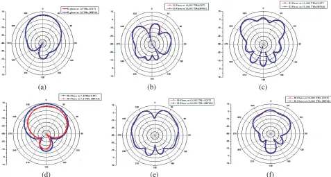
Figure 14. Radiation patterns of the antenna. (a)E-plane at 7.8 THz. (b) E-plane at 13.302 THz. (c) E-plane at 15.306 THz. (d)H-plane at 7.8 THz. (e)H-plane at 13.302 THz. (f)H-plane at 15.306 THz.
4. FREQUENCY AND GAIN TUNING TECHNIQUE
4.1. Frequency Tuning Technique
Although the following design resonates at 7.8 THz, 13.4 THz, and 15.3 THz frequencies, the resonant frequencies at multi-modes are not independently tunable. The multiband operation is because of higher-order modes. A multi-band, multi-mode antenna is attractive and useful when a single band frequency can be tuned to the desired frequency applications. Ri(i= 1,2,3) andwi (i= 1,2,3) are the most important parameters for frequency tuning. Furthermore, they have different effects on different modes. In this paper, we propose a novel technique to independently tune the resonance frequencies at multi-modes of the antenna by changing the value of radius. The return loss is shown in Figure 15. Figure 15 shows the reflection coefficient of the antenna with different values of radiusR1. IncreasingR1 makesT M11, T M02, andT M12 decrease, andT M11 and T M02 modes are decreased more than T M12. On the other hand, Figure 15(b) shows the reflection coefficient of this antenna with different values of R2 and slits (R2, W2). When increasing R2, it can be shown to decrease only T M02 and T M12. If we need to change onlyT M02, we must slightly decreaseW3, and increasedR2can be shown in Figure 15(c). Finally, with varying parameters, theT M12mode has a different change compared toT M11and T M02. According to Figure 15(c), with increasing R3 and decreasing w3, the resonance frequencies of T M11 andT M02modes stay invariant. Although all TM modes are tuned, a good agreement is shown between the two methods.
4.2. Gain Tuning Technique
Progress In Electromagnetics Research C, Vol. 96, 2019 239
(a)
(b)
(c)
Figure 15. Frequency independent tuning for (a)T M11, (b) T M02 and (c) T M12 modes.
7.8-dB. The increase of the gain is due to decreasing the current density at the following patches R2, R3 and making the electric field at the first slits, which form the increased gain at the first resonance frequency. This technology can be used at the following rings slits to increase the gain. We notice that in the thirdT M12mode when we add the slits, we can show a slight increase of the gain because of the low current density.
Figure 17 shows the input impedance characteristic of the circular ring antenna with various chemical potentials of the graphene material as a function of frequencies.
4.3. Performance Analysis of Circular Graphene Antenna
(a) (b)
Figure 16. Gain tuning for theT M11 andT M02 modes.
Figure 17. Real and imaginary part of the antenna with various chemical potentials.
Table 1. Performance comparison of the proposed antenna for add slits and various chemical potential of T M11.
Frequency TM11 Gain S11 Bandwidth frequency
Mode CST/HFSS (dB) (dB) (GHz) offset (GHz)
Add of mini-slit
Slit 1 8 −15.2 300 340
Slit 2 7.8 −13.4 287 342
Slit 3 6.5 −14 240 348
Chemical potential
[eV]
μc = 0.1 8.1 −15.01 320 500
μc = 0.2 8.15 −15 325 520
μc = 0.3 8.2 −15.2 314 512
Progress In Electromagnetics Research C, Vol. 96, 2019 241
Table 2. Performance Comparison of the proposed antenna for add slits and various chemical potential of T M02.
Frequency TM02 Gain S11 Bandwidth frequency
Mode CST/HFSS (dB) (dB) (GHz) offset (GHz)
Add of mini-Slit
Slit 1 7.95 −20 280 100
Slit 2 8.3 −26 340 122
Slit 3 6.7 −18 214 124.8
Chemical potential
[eV]
μc = 0.1 8.1 −20.2 321 120
μc = 0.2 8.15 −34 324 130
μc = 0.3 8.2 −28.6 346 131
μc = 0.4 8.23 −21.44 324.6 118.4
Table 3. Performance Comparison of the proposed antenna for add slits and various chemical potential of T M12.
Frequency TM12 Gain S11 Bandwidth frequency Mode CST/HFSS (dB) (dB) (GHz) offset (GHz)
Add of mini-Slit
Slit 1 9.2 −17 90 75
Slit 2 9.22 −18 100 78.1
Slit 3 10.24 -22 105 100
Chemical potential
[eV]
μc = 0.1 9.8 −15.3 97 90
μc = 0.2 9.7 −17.5 99.2 89.1
μc = 0.3 10.5 −20 100 89.1
μc = 0.4 11 −19.4 104.2 78.9
the previous paragraph that many results for this antenna can be changed. However, three tables are shown as follows. As we said, the addition of a mini-slit in each principal slit can be seen as a capacity. The table can show that when we add slits, we can see an increase for the gain at three resonant frequencies. In addition, the increase in the return loss is under−20 dB. On the other hand, the chemical potential has a significant role, and the increase of the chemical potential increases the gain, bandwidth, and frequency offset of the antenna, respectively. Table 1, Table 2, and Table 3 show performance comparison of the proposed antenna for adding slits and various chemical potentials of T M11,T M02, and T M12, respectively.
5. CONCLUSION
A high multiband gain SIW cavity annular ring slot antenna is proposed in this paper. Three separate operating modes are introduced by the proposed antenna with three patches like radiation patterns. However, every resonance frequency can be independently tuned, so we get a frequency offset T M11 about 540 GHz, then T M02 about 131 GHz and T M12 about 100 GHz which makes the antenna more useful for the terahertz application.
REFERENCES
1. Kyungho, H., T. K. Nguyen, I. Park, and H. Han, “Terahertz Yagi-Uda antenna for high input resistance,”J. Infrared Millim. Terahertz Waves, Vol. 31, 441–451, 2010.
2. Smith, P. R., D. H. Auston, and M. C. Nuss, “Subpicosecond photoconducting dipole antennas,”
3. Van Exter, M., C. Fattinger, and D. Grischkowsky, “Terahertz time-domain spectroscopy of water vapor,”Opt. Lett., Vol. 14, 1128–1130, 1989.
4. Wu, Q., F. G. Sun, P. Campbell, and X.-C. Zhang, “Dynamic range of an electro-optic field sensor and its imaging applications,” Appl. Phys Lett., Vol. 68, 3224–3226, 1996.
5. Jepson, P. U., R. H. Jacobsen, and S. R. Keiding, “Generation and detection of terahertz pulses from biased semiconductor antennas,”J. Opt. Soc. Amer. B, Vol. 13, 2424–2436, 1996.
6. Duvillaret, L., F. Garet, and J. L. Coutaz, “A reliable method for extraction of material parameters in terahertz time-domain spectroscopy,” IEEE J. Sel. Topics Quantum Electron., Vol. 2, No. 3, 739–746, Sep. 1996.
7. Mittleman, D., Sensing with Terahertz Radiation, Springer-Verlag, Heidelberg, Germany, 2002. 8. Nasri, A., et al., “A compact SIW mixer for millimeter-wave applications,” International Journal
of Electrical and Computer Engineering (IJECE), Vol. 4, No. 6, 902–908, 2014.
9. Doucha, S., et al., “A leaky wave antenna design based on half-mode substrate integrated waveguide technology for X band applications,”International Journal of Electrical and Computer Engineering (IJECE), Vol. 7, No. 6, 3467–3474, 2017.
10. He, Z., J. Cai, Z. Shao, X. Li, and Y. Huang, “A novel power divider integrated with SIW and DGS technology,” Progress In Electromagnetics Research, Vol. 139, 289–301, 2013.
11. Sotoodeh, Z., B. Biglarbegian, F. Hojjat-Kashani, and H. Ameri, “A novel bandpass waveguide filter structure on SIW technology,”Progress In Electromagnetics Research Letters, Vol. 2, 141–148, 2008.
12. Lin, S., S. Yang, and A. E. Fathy, ”Development of a novel UWB vivaldi antenna array using SIW technology,” Progress In Electromagnetics Research, PIER,Vol.90, 369–384, 2009.
13. Liu, Z. G. and Y. X. Guo, “Dual-band low profile antenna for body centric communications,”IEEE Trans. Antennas Propag., Vol. 61, No. 4, 2282–2285, Apr. 2013.
14. Herscovici, N., C. Christodoulou, E. Rajo-Iglesias, O. Quevedo-Teruel, and M. Sainchez-Ferflifldez, “Compact multimode patch antennas for MIMO applications,” IEEE Antennas Propag. Mag., Vol. 50, No. 2, 197–205, Apr. 2008.
15. Guan, D., Z. Qian, W. Cao, L. Ji, and Y. Zhang, “Compact SIW annular ring slot antenna with multiband multimode characteristics,” IEEE Antennas Propag. Mag., Vol. 63, No. 12, 5918–5922, Dec. 2015.
16. Ji, Y. B., et al., “Terahertz reflectometry imaging for low and high-grade gliomas,” Scientific Reports, Vol. 6, 36040, 2016.
17. Guo, W., et al., “Graphene-based broadband terahertz detector integrated with a square-spiral antenna,” Optics Letters, Vol. 43, No. 8, 1647–1650, 2018.
18. Kokotoff, D. M., J. T. Aberle, and R. B. Waterhouse, “Rigorous analysis of probe-fed printed annular ring antennas,” IEEE Trans. Antennas Propag., Vol. 47, No. 2, 384–388, Feb. 1999. 19. Shen, C., S. A. Long, M. R. Allerding, and M. D. Walton, “Resonant frequency of a circular disk,
printed circuit antenna,” IEEE Trans. Antennas Propag., Vol. 25, No. 4, 595–596, Jul. 1977. 20. Jackson, D. R., J. T. Williams, et al., “Microstrip patch design that do not excite surface waves,”
IEEE Trans. Antennas Propag., Vol. 41, 1026–1037, Aug. 1993.
21. Posadas, V. G., et al., “Approximate analysis of short-circuited ring patch antenna working at TM01 mode,”IEEE Trans. Antennas Propag., Vol. 54, 1875–1879, Jun. 2006.
22. Liu, J. H., Q. Xue, H. Wong, H. W. Lai, and Y. L. Long, “Design and, analysis of a low-profile and broadband microstrip monopolar patch antenna,”IEEE Trans. Antennas Propag., Vol. 61, No. 1, 11–18, Jan. 2013.
23. Garg, R., P. Bhartia, I. Bahl, and A.Ittipiboon, Microstrip Antenna Design Handbook, Ch. 5, 320, Artech House, Norwood, MA, USA, 2001.
24. Hanson, G. W., “Dyadic Green’s functions and guided surface waves for a surface conductivity model of graphene,”J. Ap. Phys., Vol. 103, 064302–064302, 2008.