Article
1
Modeling
dislocation
contrasts
obtained
by
2
accurate-Electron Channeling Contrast Imaging for
3
characterizing deformation mechanisms in bulk
4
materials
5
Hana KRIAA 1, Antoine GUITTON 1,2 and Nabila MALOUFI 1,2,*
6
1 Université de Lorraine - CNRS - Arts et Métiers ParisTech – LEM3, 7 rue Félix Savart, 57070 Metz, France;
7
[email protected] (H.K.); [email protected] (A.G.); [email protected]
8
(N.M.)
9
2 Laboratory of Excellence on Design of Alloy Metals for low-mAss Structures (DAMAS) – Université de
10
Lorraine, 57073 Metz, France.
11
* Correspondence: [email protected]; Tel.: +33 372 747 865
12
Received: date; Accepted: date; Published: date
13
Abstract: Electron Channeling Contrast Imaging (ECCI) is becoming a powerful tool in Materials
14
Science for characterizing deformation defects. Dislocations observed by ECCI in Scanning
15
Electron Microscope, exhibit several features depending on the crystal orientation relative to the
16
incident beam (white/black line on a dark/bright background). In order to bring new insights
17
concerning these contrasts, we report an original theoretical approach based on the dynamical
18
diffraction theory. Our calculations led, for the first time, to an explicit formulation of the
19
backscattered intensity as a function of various physical and practical parameters governing the
20
experiment. Intensity profiles are modeled for dislocations parallel to the sample surface for
21
different channeling conditions. All theoretical predictions are consistent with experimental
22
results.
23
Keywords: ECCI, dislocation contrast, modeled intensity profiles, invisibility criteria, dynamical
24
theory of electron diffraction.
25
26
1. Introduction
27
The Electron Channeling Contrast Imaging (ECCI) technique is based on the fact that the
28
BackScattered Electrons (BSE) signal is highly dependent on the orientation of the incident beam
29
relative to the lattice planes[1]. Therefore, any slight local distortion of the crystal lattice, produced
30
for instance by a dislocation, leads to a BSE intensity (IBSE) modulation, thus generating several
31
contrasts such as a bright line on a dark background [2] or a black line on a bright background [3].
32
For understanding the origin of the dislocation contrasts obtained by ECCI, the two-beam dynamical
33
diffraction theory was adapted from the Transmission Electron Microscopy (TEM) [4] [5]. Briefly, the
34
electron beams are described, inside the crystal, by a superposition of Bloch waves. The different
35
inelastic scattering events are divided into two categories: those scattered through angles less than
36
90° (forming the forward scattering wave) and those scattered through angles greater than 90°
37
(forming the backscattered wave) [6]. In the multiple scattering model electrons can be removed
38
from the forward scattering wave to the backscattered one and vice-versa. In order to simulate the
39
IBSE profiles for both perfect and imperfect crystal, Spencer et al. [7] and Wilkinson et al. [6, 8, 9] used
40
this Bloch wave-based model. They showed that for the perfect crystal, the simulated profiles exhibit
41
the main experimental features of the channeling pattern: bright band and dark edges. The same
42
approach was also used by Reimer [10, 11] for a perfect crystal where the multiple scatterings are
43
treated as incoherent. These different approaches, were extended to the case of an imperfect crystal
44
containing a dislocation [6-9] or a stacking fault [12]. Despite their contribution to the theory of
45
defects electron channeling contrasts [7-12], detailed calculations leading to an analytical expression
46
of BSE signal as a function of experimental parameters, is still missing. Furthermore, in most cases
47
[7,8] theoretical results were not compared to the experiments. This can be illustrated from the
48
dislocation profiles calculated for Bragg condition, which exhibit an extra-pic of IBSE not observed
49
experimentally [7, 8].
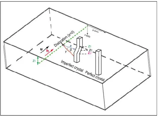
50
To deepen our understanding of the observed channeling contrast of dislocations, we propose an
51
easier way to model the IBSE as a function of physical parameters either relative to the material or
52
governing the ECCI experiment. Our theoretical results show a good agreement with the
53
experiments for several diffraction conditions.
54
In a crystal, the electronic wave function is a solution of the time independent Schrödinger’s
55
equation and is given by [11]:
56
Ψ(r) =∑jε(j)∑gCg(j)e[2πi k0
(j)
+g·r]e[-2πq(j)z]
(1)
57
The index j refers to the jth wave, ε(j) are the excitation amplitudes of the Bloch wave ψ(j), C g jare
58
the amplitudes of the diffracted waves with a wave vector kg(j) = k0 (j)
+g, where k0(j) is the wave vector
59
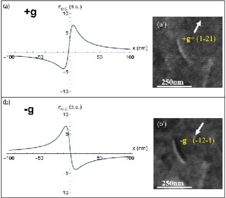
of the jth primary wave and g is the diffraction vector. r is the spatial position vector at which the
60
electron intensity is evaluated. The second factor of equation (1) contains the absorption parameter
61
q(j) expressing the exponential attenuation of the wave amplitude with increasing depth z.
62
63
In order to determine the different coefficients of the Bloch wave function, presented in equation (1),
64
Reimer used the two-beam condition i.e. only one set of lattice planes is in channeling condition.
65
Hence, the total BSE signal of a slice of a thickness dz, located at a depth z is given by [11]:
66
dη
dz = NσB {ψψ
*+ (1-∑ C 0 j
2
e[-4πq(j)z]
j )} (2)
67
N is the atom number per unit of volume, σB is the backscattering cross-section through angles
68
larger than 90° and ψψ* is the probability for the Bloch wave to be backscattered at a depth z. The
69
last terms (in parentheses) in equation (2) describe the electrons that are removed from the Bloch
70
wave field by scattering before reaching the slice dz.
71
72
The BSE coefficient ηO.C. is, then, obtained from the integration of equation (2) in the total interaction
73
depth from z=0 to z→∞ (labelled in Reimer's model). O.C. indicates that only the total BSE
74
intensity due to orientation contrast is calculated, while the contributions due to atomic number and
75
to the surface inclination are not considered [11]:
76
ηO.C. = NσB
4π ξ0 '
(-s ξg +ξ0 '
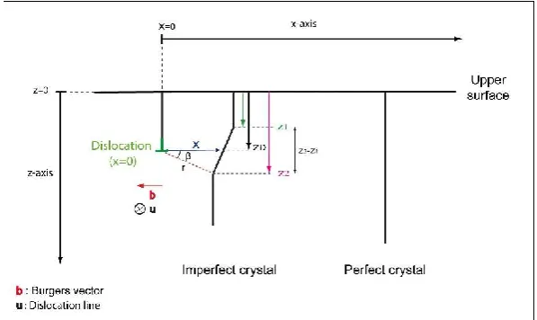
ξg'
1+(s ξg)2-(ξ0
'
ξg') 2+
s ξg
1+(s ξg)2+[(1+(s ξg)2)(ξ0 '
ξg)]
Equation (3) corresponds to the variation of the BSE intensity for a perfect crystal i.e. the intensity
78
profile of an isolated pseudo-Kikuchi band [7,11,13], where ξ '0 andξ 'g are the absorption lengths,
79
ξg is the extinction distance and s the deviation parameter.
80
81
2. Our theoretical approach for BSE intensity calculation for an imperfect crystal
82
If we consider a column located at a position x away from a dislocation, at position x=0 and depth
83
z=zD (where zD is the mean depth of the dislocation), the distortion of the lattice planes near the
84
dislocation does not depend on z but only on x and it is given by ∂R
∂z)z=zD (R is the displacement field
85
of the crystalline planes) [14].
86
Therefore, for calculating the IBSE in the case of an imperfect crystal containing a dislocation parallel
87
to the sample surface, independently of the depth z, we take into account a new deviation parameter
88
s’ written by:
89
s' = s +sD where sD = g·∂R
∂z)z=zD (4)
90
s is the deviation from the exact Bragg position in the perfect crystal, which can be experimentally
91
measured [3]. The scalar product g·∂∂zR) z=zD
represents the supplementary deviation, sD due to the
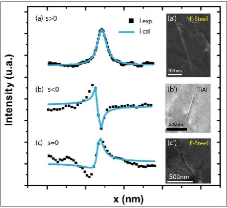
92
variation of the incidence angle between the primary beam and the distorted crystalline planes near
93
the dislocation core. Far from the dislocation, the crystal is considered perfect. The planes are not
94
distorted and the deviation sD becomes zero. Consequently, to take into account the presence of the
95
defect, we substitute s by s' in the expression of ηO.C. for a perfect crystal (in equation 3, which does
96
not depend on z). We obtain:
97
ηO.C. = Nσ4πB ξ0 '
(-(s+sD(x)z=zD)ξg+ξ0 '
ξg'
1+((s+sD(x)z=zD)ξg)2-(ξ0 '
ξg') 2+
(s+sD(x)z=zD)ξg
1+((s+sD(x)z=zD)ξg)2+[(1+((s+sD(x)z=zD)ξg)2(ξ0 '
ξg)]
2) (5)
98
This allows us to study the variation of the IBSE as a function of x (distance x away from the
99
dislocation core). Where, the contrast associated to a dislocation is described by sD (containing all
100
the effect of R).
101
2.1. Screw dislocation
102
Figure 1 shows a screw dislocation parallel to the surface of a bulk sample and located at a depth zD.
103
This defect is characterized by a Burgers vector b and a line direction u. At a distance x away from
104
the dislocation core (in x=0), the crystal plane is deformed. The displacement field Rscrew is then
105
defined in polar coordinate (ß) as follows [15]:
106
R screw = b ß 2π =
b 2π tan
-1(z-zD
x ) (6)
107
109
Figure 1. Schematic of a screw dislocation parallel to the surface and located at a depth zD. Deformed planes,
110
perpendicular to the surface, are at a distance x away from the dislocation core.
111
112
The derivative of R screw with respect to the depth z, at a turning point (z= zD), is given by:
113
dR screw
dz )z=zD = b
2πx(1+(z-zDx )
2
) )
z=zD
= b
2πx (7)
114
Based on this reasoning, the substitution of equation (7) in equation (5) allows us to obtain the
115
following expression of ηO.C.:
116
ηO.C. = NσB
4π ξ0 '
(-(s+2πxg·b )ξg+ξ0
'
ξg'
1+((s+g·b 2πx)ξg) 2
-(ξ0
'
ξg') 2+
(s+g·b 2πx)ξg
1+((s+g·b 2πx)ξg)2+{[1+((s+g·b 2πx)ξg)2(ξ0
'
ξg)}
2) (8)
117
Equation (8) gives the variation of the BSE signal as a function of the distance x and the experimental
118
parameters such as the deviation s and the diffraction vector g.
119
It should be noted that in this paper, we show profiles modeled in the case of aluminum, where the
120
parameters are: acceleration voltage E=20 kV, g= (220), the extinction distanceξg=50 nm, absorption
121
lengths ξ0'=140 nm and ξg'=600 nm [11]. It should also be mentioned that in all modeled profiles the
122
background level is taken as reference (at the zero of the ordinate axis). All negative values then
123
correspond to lower BSE intensities than the background level.
124
2.1.1. Deviation parameter s=0
125
The theoretical intensity profiles calculated from equation (8), in the case of a screw dislocation, for
126
the diffraction conditions s=0 and ±g are represented in Figure 2. Their corresponding
127
experimental ECC micrographs are also shown (Figures 2a’ and b’). The g and s vectors are,
128
respectively, determined experimentally through the pseudo-band indexation of the HR-SACP
129
(High Resolution Selected Area Channeling Pattern) assisted by EBSD experiment [2, 3].
130
131
For both +g and –g diffractions, the dislocation profiles (Figures 2.a and b) are anti-symmetric: a
132
hollow and a peak corresponding to the black and white sides of the dislocation respectively
(Figures 2a’ and b’). Moreover, in the case of –g, the extrema are inverted compared to those
134
observed for +g: the peak becomes hollow and vice versa.
135
136
Figure 2. IBSE profiles modeled, for a screw dislocation parallel to the surface, with a deviation parameter s=0
137
for the diffractions (a) +g and (b) –g with their corresponding experimental ECC micrographs (a’) and (b’).
138
139
Such theoretical results reveal that at Bragg position, a screw dislocation generates a BSE image with
140
black/white sides, which reverse with the inversion of the sign of g. Therefore, the variation of IBSE
141
given by equation (8) is in good agreement with the experimental observations already reported in
142
literature [3,7].
143
144
2.1.2. Deviation parameter s>0
145
The IBSE profiles calculated by equation (8) with a deviation parameter slightly positive (s=0.01 nm-1)
146
are represented in Figures 3a and b for the +g and –g diffractions respectively. In this condition
147
(s>0), both ±g dislocation profiles present one intensity peak only. This is in agreement with the
148
experimental ECC micrographs shown in Figures 3a’ and b’: bright line on dark background. Note
149
also that the maximum intensity does not coincide with the exact position of the dislocation core
150
(x=0 nm) but it is at x≈±4 nm: it is displaced from one side of the dislocation position to the other
151
side when changing from +g to –g. This result is analogous to that obtained in TEM and can be
152
used to characterize a dislocation configuration consisting of two parallel dislocations such as dipole
153
[3, 16].
156
Figure 3. IBSE profiles modeled, for a screw dislocation parallel to the surface, with s>0 and s<0 for (a) (c) +g
157
and (b) (d) –g with their corresponding experimental ECC micrographs (a’), (b’), (c’) and (d’).
158
2.1.3. Deviation parameter s<0
159
The IBSE profiles calculated from our theoretical model for a slightly negative deviation parameters
160
(s=-0.01 nm-1) and ±g diffraction conditions are represented in Figure 3c and 3d. For the diffraction
161
+g, the curve contains a deep hollow and a peak corresponding to the black and white dislocation
162
sides respectively (Figure 3c’). This contrast is inverted with the inversion of the sign of g (Figures
163
3d and d’). For s<0, the BSE signal emitted from the zone of interest is high: bright background.
164
2.2. Edge dislocation
165
166
Figure 4. Schematic of an edge dislocation parallel to the surface and located at a depth zD. Deformed planes,
167
perpendicular to the surface, are at a distance x away from the dislocation core.
168
Similar to the screw dislocation, an edge dislocation parallel to the surface and located at a depth zD
169
produces a local deformation of the crystalline planes nearby its core (see Figure 4). Such distortion
170
is described by its displacement field, written in polar coordinate, as follows [15]:
171
R edge=b 2π ß+
sin 2ß 2 1-ν +
bxu 2π [
1-2ν 2 1-ν ln|r|+
cos 2ß
4 1-ν ] (9)
172
173
ν is the Poisson’s ratio, u is the dislocation line direction and r is the polar coordinate. Where ß
174
and r are given by:
ß= tan-1(z-zD
x ) and r = x
cos ß (10)
176
From equations (9) and (10), R edge can be expressed as a function of the distance x away from the
177
dislocation. The new deviation parameter s' is then:
178
s' = s + g·dR edge dz )z=zD
(11)
179
180
The presence of an edge dislocation in the crystal can also be highlighted, analytically, by the
181
insertion of equation (11) in equation (5). The calculated theoretical profiles are similar to that
182
obtained for a screw dislocation. For the diffraction +g, at Bragg condition (s=0), the modeled curves
183
are characterized by a maximum and a minimum of IBSE. The edge dislocation generates a
184
white/black contrast. However, for s>0, the profile presents only a single peak consistent with
185
experimental observations. The maximum intensity is situated at a position x≈-6 nm away from
186
the dislocation core. Concerning the case of s<0, the IBSE profile show a hollow with a slight peak. All
187
profiles are also reversed, following the inversion of the g sign regardless of the deviation
188
parameter s.
189
190
2.3. Extinction criteria
191
Furthermore, for both screw and edge dislocations, considering the extinction criteria g·b =0 and
192
g·bxu =0 in our equation leads to a null BSE yield (ηO.C.=0 a.u in Figure 5a). Regarding the edge
193
dislocation, the bxu term in equation (9) becomes null when z= zD. Nevertheless, the position of the
194
dislocation is located in the [z1, z2] range (see Figure 1), therefore the bxu term is not null. For g·b =0
195
and g·bxu ≠0, in the [z1, z2] range except zD, the calculated profile for an edge dislocation displays a
196
low intensity peak ηO.C.≈2,7 (a.u) with respect to the background level) surrounded by two hollows.
197
Such residual contrast (Figure 5b) is characteristic of an edge dislocation observed by TEM under
198
these diffraction conditions [17].
199
200
Figure 5. IBSE profiles modeled for the extinction conditions: (a) g·b =0, g·bxu =0 and (b) g·b =0, g·bxu ≠0.
2.4. Quantitative comparisons with experimental profiles
203
In this part, for each deviation parameter: s>0, s<0 and s=0, an average profile is calculated from 50
204
experimental dislocation profiles and fitted by equation (5). The results are illustrated by Figures 6a,
205
b and c respectively.
206
207
Figure 6. Fitted (blue line) and experimental (black squares) IBSE profiles and their corresponding ECC
208
micrographs obtained for (a, a’): g=(01-1) and s>0, (b, b’): g=(020) and s<0 and (c, c’): g=(2-1-1) and s=0
209
respectively.
210
As can be seen, the best fits are obtained for s>0 (the correlation coefficient χ2=2) and s<0 (χ2=8.7).
211
While for s=0, the general features of the curve are well modeled, the correlation coefficient is higher:
212
χ2=16.4. At Bragg condition because of the strong interaction between the electron beam and the
213
crystal atoms [18], dynamical effects are magnified and the diffracted intensity is high enough to
214
excite neighboring reflections. Then the successively and coherently produced beams interfere with
215
each other. The "n" beam approach must thus be considered to better report the experimental results.
216
Besides, in our calculations multiple scattering was treated incoherently.
217
Nevertheless, the fitted profiles provide, among other parameters, reasonable orders of magnitude
218
of the physical parameters ξg, ξ0' and ξg' for different deviation parameters and materials
219
(interstitial Free (IF)-steel: Figure 5a, a’, c and c’ TiAl: Figures 6b and b’). Furthermore, the obtained
220
parameters are in good agreement with the values reported in the literature [11]. Such as the case of
221
IF-steel: ξg=9,4±1,3 nm ; ξ0'=170,4±36,7 nm ; ξg'=177,7±38,3 nm.
222
3. Conclusions
223
In this paper an original theoretical model based on the Bloch wave approach of the dynamical
224
diffraction theory was developed for modeling IBSE around dislocations without resorting to
225
numerical methods. An analytical formula of the BSE signal as a function of the different physical
226
parameters governing the ECCI experiment has been proposed for the first time to our knowledge.
227
The BSE contrast profiles, produced by screw and edge dislocations parallel to the sample surface,
228
display the same appearance for the diffraction conditions. For a deviation parameter s=0 (Bragg
condition) and s<0, the theoretical BSE curves show hollow and peak of intensity corresponding to
230
the black and white dislocation sides repectively. The inversion of g leads to the profile inversion
231
(hollow becomes peak and vice versa). For s>0, the bright dislocation contrast is envisaged in the
232
modeled profile by the intensity peak. This latter (dislocation image) do not coincide with the exact
233
dislocation position (x=0) and it is displaced to the opposite side when g is reversed. Moreover, our
234
theoretical model confirms the use of the invisibility criteria in ECCI.
235
The good agreement between the theoretical and experimental results was also confirmed by
236
adjusting the BSE intensity profiles. Hence, deduced values for the physical parameters ξg, the
237
extinction distance and ξ0' and ξg' , the absorption lengths are consistent with the literature.
238
Because the use of ECCI is becoming widespread for the defects characterization in bulk material in
239
SEM, we provide a usable formula of the BSE intensity produced by dislocations. Furthermore, our
240
approach can be extended to other defects. ECCI is now mature for exploring new horizons in
241
Materials Science.
242
243
Author Contributions: All ECCI observations were performed by H.K. H.K., A.G. and N.M. performed the
244
theoretical interpretations. H.K. wrote the main manuscript text. All the authors participate in the discussion.
245
Conflicts of Interest: The authors declare no conflict of interest.
246
References
247
1. Booker, G. R.; Shaw, A. M. B.; Whelan, M. J.; Hirsch, P. B. Some comments on the interpretation of the
248
Kikuchi-like reflection patterns observed by scanning electron microscopy. Phil. Mag. 1967, 16, 1185-1191.
249
2. Mansour, H.; Guyon, J.; Crimp, M. A.; Gey, N.; Beausir, B.; Maloufi, N. Accurate electron channeling
250
contrast analysis of dislocations in fine grained bulk materials. Scripta. Mater. 2014, 84-85, 11-14.
251
3. Kriaa, H.; Guitton, A.; Maloufi, N. Fundamental and experimental aspects of diffraction for
252
characterizing dislocations by electron channeling contrast imaging in scanning electron microscope. Sci.
253
Rep. 2017, 7, 9742.
254
4. Howie, A.; Whelan, M. J. Diffraction contrast of electron microscope images of crystal lattice defects. II.
255
The development of a dynamical theory. Proc. Royal. Soc. 1961, 263, 217-237.
256
5. Howie, A.; Whelan, M. J. Diffraction contrast of electron microscope images of crystal lattice defects. III.
257
Results and experimental confirmation of the dynamical theory of dislocation image contrast. Proc.
258
Royal. Soc. 1962, 267, 206-230.
259
6. Wilkinson, A. J.; Hirsch, P. B. Electron diffraction based techniques in scanning electron microscopy of
260
bulk materials. Micron. 1997, 28, 279-308.
261
7. Spencer, J. P.; Humphreys, C. J.; Hirsch, P. B. A dynamical theory for the contrast of perfect and imperfect
262
crystals in the scanning electron microscope using backscattered electrons. Phil Mag. 1972, 26:1, 193-213.
263
8. Wilkinson, A. J.; Hirsch, P. B.; Czernuszka, J. T.; Long, N. J. Electron channeling contrast imaging of
264
defects in semi-conductors. Proc. Micros. Semiconduct. Mater. 1993, 134, 755-762.
265
9. Wilkinson, A. J.; Hirsch, P. B. The effects of surface stress relaxation on electron channelling contrast
266
images of dislocations. Phil. Mag. A. 1995, 72:1, 81-103.
267
10. Reimer, L.; Heilers, U.; Saliger, G. Kikuchi band contrast in diffraction patterns recorded by transmitted
268
11. Reimer, L. Scanning Electron Microscopy. Physics of image formation and microanalysis.
270
Springer-Verlag Berlin Heidelberg GmbH, 2nd edition (1998).
271
12. Zeafferer, S.; Elhami, N. N. Theory and application of electron channelling contrast imaging under
272
controlled diffraction conditions. Acta. Mat. 2014, 75, 20-50.
273
13. Clarke, D. R.; Howie, A. Calculations of lattice defect images for scanning electron microscopy. Phil. Mag.
274
1971, 24 (190), 959-971.
275
14. Cockayne, D. J. H.; Ray, I. L. F.; Whelan, M. J. Investigations of dislocation strain fields using weak beams.
276
Phil. Mag. 1969, 20-168, 1265-1270.
277
15. Hirth, J. P.; Lothe, J. Theory of dislocations. A Wiley-Interscience Publication, 2nd edition (1982).
278
16. Guitton, A. Joulain, A. Thilly, L. Tromas, C. Dislocation analysis of Ti2AlN deformed at room
279
temperature under confining pressure. Sci. Rep. 2014, 4 (6358), 1-4.
280
17. Edington, J. W. Interpretation of Transmission Electron Micrographs. London (1976).
281
18. Williams, D.B.; Carter, C. Transmission Electron Microscopy. Springer, New York (1996).