Reducing Energy Consumption in Network-on-Chip
by using Data Encoding Technique
Mrs.
S.Sandhya
1, K.Ravitheja
21
Assistant professor, Department of ECE, Adams engineering College, Khammam Telangana.
2
M-Tech Student Department of ECE, Adams engineering College, Khammam Telangana.
Abstract: The power dissipated by the links of a network-on-chip.the power dissipated by the other elements of the communication subsystem, namely, the routers and the network interfaces. we present a set of data encoding schemes to reduces the power dissipated by he links of an Network on chip. In proposed schemes are general and transparent with respect to the Network on chip (i.e., their application does not require any modification of the routers and architecture). We shows the both synthetic and real traffic scenarios of the effectiveness of the proposed schemes, which allow to save up to 51% of power dissipation and 14% of energy consumption without any significant performance degradation and less than 15% area overhead in network interface.
Keywords:Coupling switching activity, data encoding, interconnection on chip, low power network-on-chip,power analysis
I.
INTRODUCTION
SHIFTING from a silicon technology the results in faster and more power efficient gates but slow and more power hungry wires[1]. In this, more than 50% of the dynamic power is dissipated through interconnects in current processors, and this is expected to rise to 65%–80%of the next several years [2]. Global interconnect length does not suitable for smaller transistors and local wires. Chip size remains constant because the chip function continuously increase the RC delay and increases exponentially. At 32/28 nm, the RC delay in a 1-mm global wire at the minimum pitch is 25× higher than the intrinsic delay of a two-input NAND gate. If the raw computation the ability of instancing more and more cores in a single silicon die, it increasing the scalability issues, due to the efficient and reliable communication between increasing the no of cores is the real problem[3] the scalability and variability issues that characterize the ultra deep submicron meter era in Nowadays, the on-chip communication issues as relevant as, in some cases more relevant than, the computation-related issues [4]. In fact, the communication subsystem increases impacts in the traditional design objectives, including cost, area, performance, power dissipation, energy consumption, reliability, etc. As technology shrinks, the more significant fraction of the total power budget is complex in system-on-chip. In this paper, we focus on aimed to reducing the power dissipated by the network links. In fact, the power dissipated by the network links by routers and network interfaces and their contributions to increase the technology scale
In particular, we present a set of data encoding schemes operating at flit level and on an end-to-end basis, which allows us to minimize both the switching activity and the coupling switching activity on links of the routing paths traversed by the packets. The proposed encoding schemes, which are transparent with respect to the router implementation, are presented and discussed at both the algorithmic level and the architectural level, and assessed by means of simulation on synthetic and real traffic scenarios. The analysis takes into account several aspects and metrics of the design, including silicon area, power dissipation, and energy consumption. The results show that by using the proposed encoding schemes up to 51% of power and up to
degradation in performance and with 15% area overhead in the NI. The rest of this paper is organized as follows. We briefly discuss related works in Section II, while Section III presents an overview of the proposed data encoding schemes. The proposed data encoding schemes along with possible hardware implementations and their analysis are described in Section IV. In Section V, the results for the hardware overhead, power and energy savings, and performance reduction of the proposed data encoding schemes are compared with those of other approaches. Finally, this paper is concluded in Section VI.
II. RELATED WORKS AND CONTRIBUTIONS
In the next several years, the availability of chips with 1000cores is foreseen [6]. In these chips, total system power budget is dissipated by interconnection networks. The design of power-efficient interconnection networks has been focus of many works in the literature dealing with Network on chip architectures. These works concentrate on different components of the interconnection networks such as routers, NIs, and links. The data encoding scheme is another method it is to reduce the link power dissipation. The data encoding techniques may be classified into two categories. In the first category, encoding techniques concentrate on lowering the power due to self-switching activity of individual bus lines while ignoring the power dissipation owing to their coupling switching activity. In this category, we proposed the bus invert (BI) and INC- XOR have data patterns and graycode are used in encoding techniques. the power consumption due to the coupling switching activity to become a large fraction of the total link power consumption. The works in the second category concentrate on reducing power dissipation through the reduction of the coupling switching [10], Among these schemes [10], the switching activity is reduced using many extra control lines. first the data both odd and even inverted number then transmission is performed using the kind of inversion which
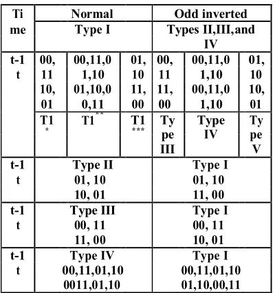
Ti Normal Odd inverted
me Type I Types II,III,and
IV
t-1 00, 00,11,0 01, 00, 00,11,0 01,
t 11 1,10 10 11 1,10 10
10, 01,10,0 11, 11, 00,11,0 10,
01 0,11 00 00 1,10 01
T1 T1** T1 Ty Type Ty
* *** pe IV pe
III V
t-1 Type II Type I
t 01, 10 01, 10
10, 01 11, 00
t-1 Type III Type I
t 00, 11 00, 11
11, 00 10, 01
t-1 Type IV Type I
t 00,11,01,10 00,11,01,10
0011,01,10 01,10,00,11
TABLE 1 EFFECT OF ODD INVERSION ON CHANGE OF TRANSITION TYPES
The basic idea of the proposed approach is encoding the flits before they are injected into the network with is to minimizing the self-switching activity and the coupling switching activity traversed by the flits and self-switching activity and coupling switching activity are responsible for link power dissipation. In this paper, we refer the end-to-end scheme. It takes advantage of the pipeline nature of the wormhole switching technique [4].for the proposed scheme, an encoder and a decoder block are added to the network interface.
III. OVERVIEW OF THE P ROPOSAL
The basic idea of the proposed approach is encoding the flits before they are injected into the network with the goal of minimizing the self-switching activity and the coupling switching activity in the links traversed by the flits. In fact, self-switching activity and coupling switching activity are responsible for link power dissipation. In this paper, we refer to the end-to-end scheme. This end-to-end encoding technique takes advantage of the pipeline nature of the wormhole switching technique [4].Note that since the same sequence of flits passes through all the links of the routing path, the encoding decision taken at the NI may provide the same power saving for all the links.For the proposed scheme, an encoder and a decoder block are added to the NI. Except for the header flit, the encoder encodes the outgoing flits of the packet such that the power dissipated by the inter-router point-to-point link is minimized.
IV. ROPOSED ENCODING SCHEMES
The proposed encoding scheme is to reduce power dissipation by minimizing the coupling transition activities
and interconnection network . The dynamic power dissipated by the interconnects and drivers is
P =[T0→1(CS+Cl)+TCCC]V2dd Fck (1)
where T 0→1 is the number of 0 transitions in the bus in two
consecutive transmissions, T c is the number
of correlated switching between physically adjacent lines, C s is the line to substrate capacitance, C l is the load capacitance, C is the coupling capacitance, Vdd is the supply voltage, and F ck is the clock frequency. A Type I transition occurs when one of the lines switches when the other remains unchanged. In a Type II transition, one line switches from low to high while the other makes transition from high to low. A Type III transition corresponds to the case where both lines switch simultaneously. Finally, in a Type IV transition both lines does not change. The coupling transition activity, T c , is a weighted sum of different types of coupling transition contributions.Therefore
TC =K1T1+K2T2+K3T3+K4T4 (2)
Using (2), one may express (1) as
P =[T0→1(Cs+Cl)+(T1+2T2)Cc]v2ddFck (3)
PαT0→1Cs+(T1+2T2)Cc (4)
we calculate the occurrence probability for different types of transitions. Consider that flit (t − 1) and flit(t) refer to the previous flit which was transferred the link in the flit respectively. We consider only two adjacent bits of the physical channel. Sixteen different combinations of these four bits could occur(Table I). the first bit is the value of the generic ith line of the link, whereas the second bit represents the value of its (i +1)th line. The number of transitions for Types I, II, III, and IV are 8, 2, 2, and 4, respectively. For a random set of data, each of these sixteen transitions has the same probability. Therefore, the occurrence probability in Types I, II, III, and IV are 1/2, 1/8, 1/8, and 1/4, respectively.
A scheme1
In scheme I, we focus on reducing the numbers of Type I transitions and Type II by converting in to type1. The scheme compares the current data with the previous one to decide whether odd inversion or no inversion of the current data can lead to the link power reduction.
P’αT0→1+(K1T1’+K2T2’+K3T3’+K4T4’)CC (5)
Figere.1(a).Encoder architecture scheme I circuit diagram
Fig.1.(b) encoder architecture scheme1 internal view of the encoder block(E)
Proposed Encoding Architecture:
The proposed encoding architecture, which is based on the odd invert condition defined by is shown in Fig. 1. We consider a link width of w bits. If no encoding is used. The w-1 bits of the incoming (previous encoded) body flit are indicated by X i (Y i ), i = 0,1,...,w − 2. The wth bit of the previously encoded body flit is indicated by inv which shows if it was inverted (inv = 1) or left as it was (inv= 0)
B. Scheme II
In the proposed encoding scheme II, we make use of both odd and full inversion. The full inversion operation converts Type II transitions to Type IV transitions. The scheme compares the current data with the previous one to decide whether the odd, full, or no inversion of the current data of power reduction.
1)Power model: The odd inversion leads to power reduction when p’< p’’ and p’< p. the power p’’ is given by
P’’ α T1+2T4** (13)
T2+T3+T4+2T1 ***
<T1+2T4 **
(14)
2(T2-T4**) <2Ty-w+1 (15)
Based on (12) and (15), the odd inversion condition is obtained as
2(T2-T4**)<2Ty-w+1 Ty>(w-1)/2 (16)
T2>T4 **
(17) 2(T2-T4**)>2Ty-w+1 T2>T4** (18)
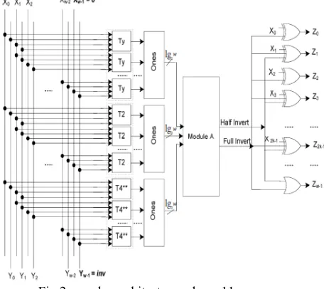
Proposed Encoding Architecture: The operating an encoder implementing the Scheme1in proposed encoding architecture, which is based on the odd invert condition of and the full invert condition of is shown in Fig. 2. Here again, the wth bit of the previously and the full invert condition of is shown in Fig. 2 In this encoder, in addition to the T y block in the Scheme I encoder, we
have the T 2 and T ∗∗4 blocks which determine if the inversion based on the transition types T 2 and T ∗∗4 should be taken place for the link power reduction. The second stage is formed by a set of 1s blocks which count the number of 1s in their inputs. The output of these blocks has the width of log 2 w.
Fig.2.encoder architecture scheme11
Finally, the bottom 1s block specifies the number of transitions whose full inverting of pair bits leads to the increased link power. Based on the number of 1s for each transition type, Module A decides if an odd invert or full invert action should be performed for the power reduction.
Fig.3.(b) decoder architecture scheme2 internal view of decoder block(D).
For this module, if is satisfied, the corresponding output signal will become “1.” In case no invert action should be taken place, none of the output is set to “1.” Module A can be
implemented using full-adder and comparator blocks. The circuit diagram of the decoder is shown in Fig. 3.
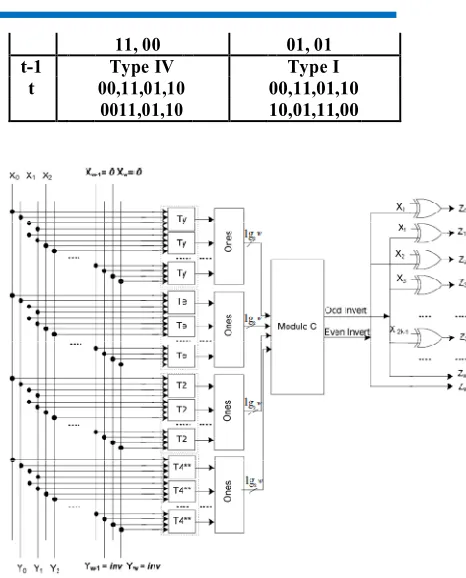
C. Scheme III
In the proposed encoding Scheme III, we add even inversion to Scheme II. The reason is that odd inversion converts some of Type I (T ∗∗∗1) transitions to Type II transitions. As can be observed from Table II, if the flit is even inverted, the transitions indicated as T ∗∗1/T ∗∗∗1 in the table are converted to Type IV/Type III transitions.
1)Power model: similar to the analysis given for scheme1,we approximate the condition p’’’< p as
T1+2T2>T2+T3+T4+2T1 *
(19)
Defining
Te = T2+T1-T1* (20)
Ti Normal Even inverted
me Type I Types II,III,and
IV
t-1 01, 00,11,0 00, 01, 00,11,0 00,
t 10 1,10 10 10 1,10 11
00, 10,01,1 01, 10, 00,11,0 11,
11 1,00 10 01 1,10 00
T1 T1** T1 Ty Type Ty
* ***
pe IV pe
II III
t-1 Type II Type I
t 01, 10 01, 10
10, 01 11, 00
t-1 Type III Type I
t 00, 11 00, 11
11, 00 01, 01
t-1 Type IV Type I
t 00,11,01,10 00,11,01,10
0011,01,10 10,01,11,00
Fig. 4. Encoder architecture Scheme III.
2) Proposed Encoding Architecture: The operating principles of this encoder are similar to those of the encoders implementing Schemes I and II. The proposed encoding architecture, which is based on the even invert condition.
In Fig.4 the first stage, we have added the T e blocks which determine if any of the transition types of T2,T ∗∗1, and T ∗∗∗1 is detected for each pair bits of their inputs. For these transition types, the even invert action yields link power reduction. Again, we have four Ones blocks to determine the number detected transitions for each. The output of the Ones blocks are inputs for Module C.
V. RESULTS AND DISCUSSION
700 MHz).
The encoder and the decoder were designed in Verilog HDL described at the RTL level, synthesized with synopsys design compiler and mapped onto an UMC 65-nm technology library. the proposed encoding scheme I (H), scheme II (HF), and scheme III (OEF) are compared against SC and SCS [23], the BI coding the coupling driven BI (CDBI) coding and the forbidden pattern condition (FPC) codes.
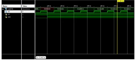
Fig. 5. RTL schematic for scheme1
Fig. 6. Simulation results for scheme1
VI. CONCLUSION
We have presented a set of data encoding schemes aimed at reducing the power dissipated by the links of an NOC. In fact, the overall power dissipated by the communication system. As compared to the previous encoding schemes proposed in the literature, the proposed schemes is to minimize not only the switching activity, but also the coupling switching activity which is mainly responsible for link power dissipation in the deep sub micro meter technology. The proposed encoding schemes are agnostic to NOC architecture in the sense that their application does not require any modification neither in the routers nor in the links. An extensive evaluation has been carried out to assess the impact of the encoder and decoder logic in the Network Interface. It impacts the performance, power, and energy. The application of the proposed encoding schemes allows savings up to 51% of power dissipation and 14% of energy consumption without any significant performance degradation and less than 15% area overhead in the Network Interface.
REFERENCE:
[1] International Technology Roadmap for Semiconductors. (2011) [Online].Available: http://www.itrs.net
[2] M. S. Rahaman and M. H. Chowdhury,
“Crosstalk avoidance and errorcorrection coding for coupled RLC interconnects,” in Proc. IEEE Int Symp. Circuits Syst., May 2009, pp. 141–144.
[3] W. Wolf, A. A. Jerraya, and G. Martin,
“Multiprocessor system-on-chipN MPSoC technology,” IEEE Trans. Comput.-Aided Design Integr. Circuits Syst., vol. 27, no. 10, pp. 1701–1713, Oct. 2008.
[4] L. Benini and G. De Micheli, “Networks on chips: A new SoC paradigm,” Computer, vol. 35, no. 1, pp. 70– 78, Jan. 2002.
[5] S. E. Lee and N. Bagherzadeh, “A variable frequency link for a power aware network-on-chip (NoC),” Integr. VLSI J., vol. 42, no. 4,pp. 479–485, Sep. 2009. [6] D. Yeh, L. S. Peh, S. Borkar, J. Darringer, A. Agarwal,
and W. M. Hwu, “Thousand-core chips roundtable,” IEEE Design Test
Comput., vol. 25, no. 3, pp. 272–278, May Jun. 2008. [7] A. Vittal and M. Marek-Sadowska,
“Crosstalk reduction for VLSI,” IEEE Trans. [8]
M. Ghoneima, Y. I. Ismail, M. M. Khellah, J. W. Tschanz, and V. De, “Formal derivation of optimal active shielding for low-power on-chip buses,” IEEE Trans.
Computer Aided Design Integr. Circuits Syst., vol. 25, no. 5, pp. 821–836, May 2006.
[9] L.Macchiarulo, E. Macii, and M. Poncino,
“Wire placement for crosstalk energy minimization in address buses,” in Proc.
Design Autom. Test Eur. Conf. Exhibit., Mar. 2002, pp. 158–162.
[10] R. Ayoub and A. Orailoglu, “A unified transformational approach for reductions in fault vulnerability, power, and crosstalk noise and delay on processor buses,” in
Proc. Design Autom. Conf. Asia South Pacific, vol.2. Jan. 2005, pp. 729–734.
degree in Electronics and communication Engineering & M.Tech PG in VLSI system design from JNTUH, Hyderabad. She is expert in VLSI Design and Digital communication. She is currently working as An Assistant Professor in ECE Department in Adam’s Engineering College, Paloncha, Khammam, Telangana State ,India. mail id: [email protected]
Mr. K.RAVITHEJA M.TECH (VLSI system design ) PURSUING In Adam’s Engineering College, Paloncha, Khammam DIST, TELANGANA, INDIA.