Design of BIST Architecture of 8×8 SRAM
Testing using Transient Current Method
Rohit Jain
1, Rajesh Khatri
2PG Student [Microelectronics & VLSI Design], Dept. of E&I Engineering, SGSITS Indore, MP, India1 Assistant Professor, Dept. of E&I Engineering, SGSITS Indore, MP, India2
ABSTRACT:BIST Architecture is proposed in this paper for testing of 8×8 SRAM based on transient current method. Basically in this method comparison is made between the faulty SRAM & non faulty SRAM by conversing transient current into voltage. The fault is detected by mismatched waveform of transient voltage. This method is faster than the March Algorithm method. In transient current method only 2 write operations are required instead of 4 as in March Algorithm method. Transient current method is low power technology. All the simulations i.e. write operation, transient current and transient voltage is carried out on 6T SRAM cell. Simulations are carried out on 8×8 SRAM circuit & are designed on Cadence UMC 180nm process technology file with supply voltage 2.5V. Cadence specter simulator is used to simulate proposed BIST.
KEYWORDS: SRAM, March Algorithm, IDDT current, Vddt Sensor, Decoder, BIST.
I.INTRODUCTION
Memories are important part of System on chip (SOCs). The forecast for 2013 from International Technology Roadmap for semiconductors (ITRS) [1][2] states that the 90% of the area of SOCs will be made up of memories, mostly static Random Access Memory. To improve the system performance large array SRAMs is very helpful. In SRAM testing various fault models such as transition fault, Open defect fault, Bridging fault and Stuck at fault needed to be used. To detect these fault March Algorithm [3][4] is widely used. But it is time consuming process. March Algorithm requires 4 write operations, but IDDT method takes 2 write operations. So that IDDT current method is faster than March Algorithm. In Transient current method there are many parameters of waveform that may be change. In transient current testing, there are usually measured parameters (Fig 1), which include current waveform width, the peak value of waveform, changed provided by waveform, the time at which the waveform reaches its peak value and the peak value of waveform. Testing using quiescent current (IDDQ) is also used [5]. Some defects in SRAM may not be detected by using IDDQ. But all open defect fault is detected in SRAM cell by monitoring a transient current pulse during a write or read operation.
In this paper transient current method is used in order to experimentally analyze electrically defects in SRAMs. All possible defects in the memory cell array will be given, together with a systematic way of reducing the number of simulated defects. SPICE simulation will be performed, and the behaviours will be transformed into functional fault models.
This paper is organised as follows: section II established designing of SRAM cell, section III describe, how to transient current flow in SRAM cell and types of faults, section BIST architecture of SRAM is designed, section V show the faults in SRAM based on simulation result, section VI ends with conclusion.
II.BACKGROUND
A. SRAM Cell:
Figure 1: 6T CMOS SRAM cell
Where,
PR =W6/L6
W4/L4
If L4=L6=180nm
Then,
PR =W6
W4
PR has to be at least less than 1.8 to ensure the write stability. A PR value of 1 is chosen for design of 6T cell. Then
W4 = W6 = 240nm
For read stability the voltage v1 across M1 is less than the threshold voltage (=0.4v).It can be chosen by the
size of M1 and M3. The exact size of M1 & M3 is determined by Cell Ratio (CR).
Where,
CR =W1/L1
W3/L3
If L1=L5=180nm
Then,
CR =W1
W3
CR has to be greater than 1.2 to ensure the read stability. A CR value of 1.2 is chosen for design of 6T SRAM cell.
B. Transient current:
Basically transient current flow in SRAM, when direct current flow between Vdd and ground in combination
with the charging and discharging of node capacitance.
Now consider the write "0" operation, assuming that logic "1" is stored in the SRAM cell initially. Figure shows the voltage levels in the CMOS SRAM cell at the beginning of the data-write operation. The transistors M1 and
M6 are turned off, while the transistors M2 and M5 operate in the linear mode. The current through M5 and M2 is
transient current. These current directly flow from Vdd to ground. This is shown in figure 2.
Figure 2: Transient current in SRAM cell [7]
C. Fault introduced:
The Fault occurs in SRAM cell due to logical or electrical design errors and faults in fabrication due to stressful operating conditions, namely reliability problem. Faults in fabrication are fault that were not intended. The faults in fabrication are occurring due to mistake in fabrication process or designing problem. The testing mechanism is based on comparison between logical behaviour of good SRAM cell and faulty SRAM cell. The fault in SRAM cell occurs due to open and bridging fault shown in figure 3.
Figure 3: Open and bridging fault in SRAM cell [8]
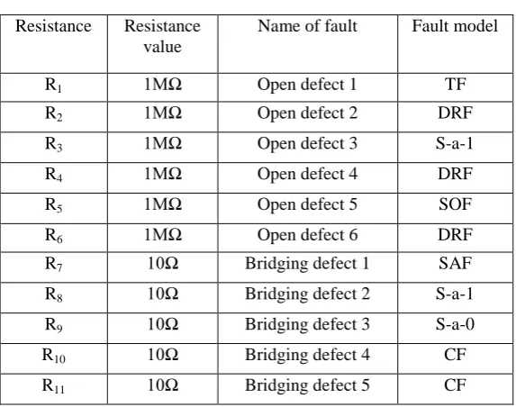
Table I
Resistance introduced to fault model
Resistance Resistance value
Name of fault Fault model
R1 1MΩ Open defect 1 TF
R2 1MΩ Open defect 2 DRF
R3 1MΩ Open defect 3 S-a-1
R4 1MΩ Open defect 4 DRF
R5 1MΩ Open defect 5 SOF
R6 1MΩ Open defect 6 DRF
R7 10Ω Bridging defect 1 SAF
R8 10Ω Bridging defect 2 S-a-1
R9 10Ω Bridging defect 3 S-a-0
R10 10Ω Bridging defect 4 CF
R11 10Ω Bridging defect 5 CF
SAF: Stuck at fault occure in SRAM cell, when it has always zero or has always one. Stuck at faults are represents by S-a-0 and S-a-1.
TF: Transition fault in SRAM, when it makes a transition 0-1 or 1-0 but fails to other direction.
SOF: Stuck open fault occure in SRAM cell when it has the unexpected result, i.e. niether write nor read operation.
CF: Coupling fault in SRAM cell is considered, when write operation to the cell affects the contents of nieghbouring cell vice versa.
DRF: Data retaction fault is occure when it loses its content after certain period.
IV. BIST ARCHITECTURE
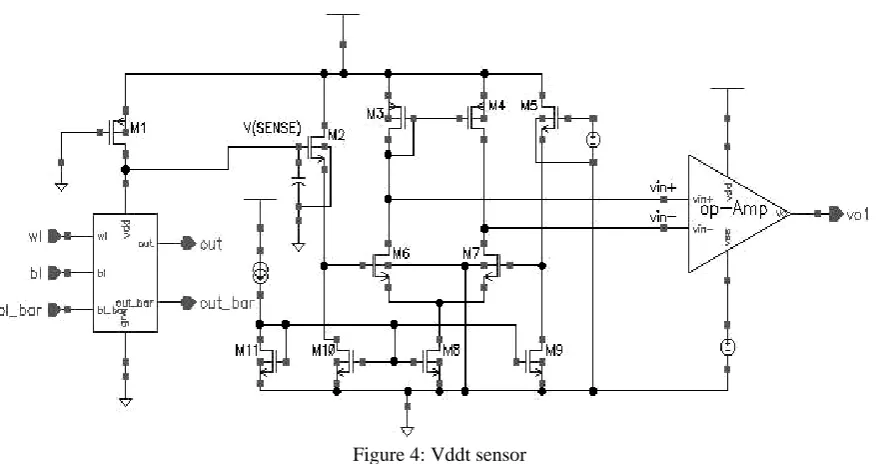
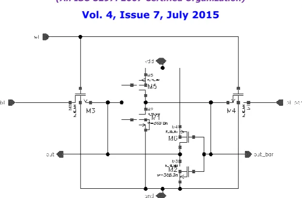
A. Vddt sensor:
IDDT current [9][10] is very fast action. It is extremely difficult to sense and process it. Mostly in low power technologies, processing the dynamic supply current is almost insoluble. Thus by transforming the current to voltage, and handling the resulted voltage waveform is a possible solution.
The Vddt sensor has a PMOS transistor, which have grounded gate, which acts like a low value resistance. 1pf value of capacitor is used; the Vddt sensor is shown in figure 4. M2 and M5 act as two emitter follower, which have same DC
condition.
Then current through M2 and M5 are also identical. Here capacitor C is used to stretch the voltage at V
Figure 4: Vddt sensor
In Vddt sensor all transistors should be in saturation, sizing of transistor shown in given table III.
TABLE II.
SIZING OF TRANSISTOR
Transistor Width of transistor (W in µm)
Length of transistor (L in µm
) M1 10 180
M2 8 180
M3 6 180
M4 4 180
M5 8 180
M6 4 180
M7 4 180
M8 0.24 180
M9 0.24 180
M10 0.48 180
M11 1 180
B. Testing circuitry of SRAM:
Figure 5: BIST circuitry
C. Test for faulty SRAM array:
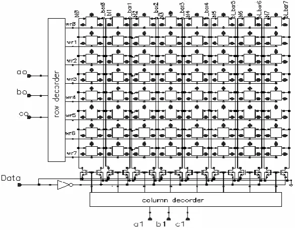
A Block level representation of the entire memory system [11] is shown in figure 6.The BIST architecture in the in same row share same word line. The 8×8 BIST architecture for SRAM is made by 64 bit BIST architecture. Here two decoders are used, which are column decoder and row decoder. Column decoder selects the bl and bl_bar and row decoder is used to select the word line (wl). The block level representation of memory system with testing circuit is shown in figure 6. The output of the particular BIST architecture gives the constant output or pulse output. If output is constant, i.e. the SRAM is non faulty otherwise SRAM is faulty.
IV.SIMULATION RESULT
A. Sensor output:
During the write operation, changes of state 0 to 1 or 1 to 0 in SRAM cell will cause the transient current to flow in SRAM cell. This transient current flows in good SRAM cell, which is shown in figure 7.
Figure 7: Transient current for good SRAM cell
This transient current is also flow in faulty SRAM cell flow in faulty SRAM cell, which is different from good SRAM cell. This is shown in figure 8.
Figure 8: Transient current for good SRAM cell
PMOS M1 senses the transient current. Due to these transient current, small spikes occurs at V (SENSE). This V
(SENSE) voltage given to differential amplifier and output of differential amplifier is amplified by the amplifier. If SRAM cell is non faulty, then output of Vddt sensor circuit shown in figure 9.
Figure 9: Vddt sensor output voltage for good SRAM cell
Figure 10: Vddt sensor output voltage for faulty SRAM cell
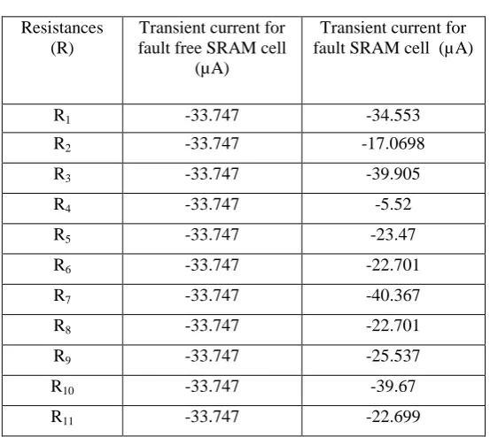
B. Test for with single fault:
The test is performed with single fault, which is introduce by different value of resistance, then open and bridging faults are introduce individually. The difference in transient current between a faulty and fault free SRAM cell are shown in table II.
TABLE II.
TRANSIENT CURRENT FOR SINGLE FAULT
Resistances (R)
Transient current for fault free SRAM cell
(µA)
Transient current for fault SRAM cell (µA)
R1 -33.747 -34.553
R2 -33.747 -17.0698
R3 -33.747 -39.905
R4 -33.747 -5.52
R5 -33.747 -23.47
R6 -33.747 -22.701
R7 -33.747 -40.367
R8 -33.747 -22.701
R9 -33.747 -25.537
R10 -33.747 -39.67
R11 -33.747 -22.699
C. Output of BIST architecture:
Figure 11: Output of BIST circuit for under test non faulty SRAM cell
If under test SRAM cell is faulty, then output of BIST architecture is a pulses output
. Figure 12 shows the
output put of BIST architecture with comparing to good SRAM cell and faulty SRAM cell.
Figure 12. Output of BIST circuit for under test faulty SRAM cell
V. CONCLUSION
In this research a BIST architecture using transient current method approach for fault detection is implemented and its effectiveness has been tested simple memory architecture with single or multiple faults, and also testing to large array of memory BIST architectures.
In perspective of future work on this project the consumption of BIST of SRAM for observing fault for such large array of memory, can be reduced by implementing a separate block for collective testing methodology for each block at once.
REFERENCES
[1] “International Technology Roadmap for semiconductors,” Semiconductor Industry Association, 2003. [2] “International Technology Roadmap for semiconductors,” Semiconductor Industry Association, 2005. [3]Van de Goor, “Using March Test to test SRAMs,” IEEE Design and Test of computers, pp. 8-14, March 1993. [4] Luigi Dilillo, Patrick Girard, “Dynamic Read Destructive in embedded-SRAM: Analysis and March Test Solution,”
[7] Sung-Mo Kang, Yusuf Leblebici, “CMOS Digital Integrated Circuits Analysis and Design,” Third Edition, pp. 438-445.
[8] Anumol K A, N.M.Siva Mangai, P.Karthigai Kumar, “Built in Self Test Architecture for Testing SRAM Using Transient Current Testing,” IEEE Conference on Information and Communication Technologies, pp. 331-335, 2013.
[9] Suriya A. Kumar, Rafic Z. Makki, and David Binkley, “IDDT Testing of CMOS Embedded SRAMs,” Design, Automation and Test in Europe Conference and Exhibition, Proceedings, 2002.
[10] Doe Yoon , Hong-Sik Kim, and Sungho Kang, “Dynamic Power Supply Current Testing for Open Defects in CMOS SRAMs,” ETRI Journal, Volume 23, Number 2, pp., 77-84, June 2001.
![Figure 3: Open and bridging fault in SRAM cell [8]](https://thumb-us.123doks.com/thumbv2/123dok_us/7785757.1287942/3.595.155.442.537.710/figure-open-bridging-fault-sram-cell.webp)