Grid Interfacing Three Phase Five-Level Inverter
with Less Number of Switching Elements
Dr Pagidimarri Krishna, Professor in EEE Dept., Nalla Malla Reddy Engineering
College (NMREC), Hyderabad.
Tadakamalla Sudarshana Rao, Asst. Professor in EEE Dept., Nalla Malla Reddy Engineering
College (NMREC),
Madhukar Challa, Asst. Professor in EEE Dept.,
Jyothishmathi institute of Technology & Science,
Karimnagar.
Abstract- Induction mot ors are widely used in indust ries, because they are rugged, reliable and economical and hence they are called as work horse power of industry . Induct ion mot or drives requires suitable converters to get the required speed and t orque without or negligible ripples. Multilevel inverters can do t his job. But the conventional MLIs such as Diode Clamp ed M LIs requires extra diodes in conjunct ion wit h t he act ive switches, Flying capacitor MLIs requires extra Capacit ors and control also difficult if the levels increases and the Cascaded H -bridge MLIs requires separate dc sources which limits it s use. T his paper p rop oses a new t y p e of mult i level Invert er emp loying PWM technique which converts the dc into ac using less number of swit ches when comp ared t o convent ional multilevel Inverters. Finally the induction motor using proposed inverter is simulated using Matlab/Simulink environment and t he corresp onding result s are p resent ed in t his p ap er.
Keywords- Multi-Level Inverters, Grid Connect ion, PWM .
I.INTRODUCTION
The AC induction motor is a rotating electric machine designed to operate a three-phase source of alternating voltage. The AC induction motor (ACIM) is the most popular motor used in consumer and industrial applications, and represented the "muscle" behind the industrial revolution. The induction motor is always rotating at synchronous speed; hence to get the speed control we need control the both voltage and frequency. By choosing the suitable inverter [1] we can vary both voltage and frequency of the induction motor to get the required speed control. Normally the conventional H-bridge inverter produces a square output, which contains infinite number of odd harmonics and dv/dt stress is also high. Normal PWM inverter [2] can reduces the THD, but
switching losses are high and also this inverter is restricted to low power applications. The importance of multilevel inverters [MLI] has been increased since last few decades [3], [4]. These new types of inverters are suitable for high voltage and high power application due to their ability to synthesize waveforms with better harmonic spectrum and with less THD. Generally MLIs are classified into three types: they are 1.Diode Clamped MLIs 2. Flying capacitor MLIs 3. Cascaded H-bridge MLIs. Diode clamped MLIs require large number of clamping diodes [5] as the level increases. In flying capacitor MLIs, Switching utilization and efficiency [6, 7] are poor and also it requires large number of capacitors as the level increases and cost is also high. Cascaded H-bridge MLIs are mostly preferred [8] for high power applications as the regulation of the DC bus is simple. But it requires separate dc sources and also the complexity of the structure is increases as the level predominantly increase. In order to address the above concerns, this paper proposes a new type of multilevel inverter which requires less number of DC sources and switches compared to Cascaded H-bridge MLIs.
II. OPERATIONAL PRINCIPLE OF THE PROPOSED INVERTER
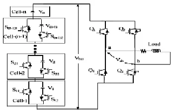
Figure 1 shows the proposed structure single phase MLI inverter. It consists of ‘n’ cells of switch circuits. For cells from ‘1’ to (n-1), each k-cell is composed of one dc voltage source and two switches (Sk1,Sk2); one switch
(Sk2) is connected in series with a dc voltage source and
the other switch (Sk1) is connected in parallel with both
Figure 1: Structure of T he Proposed Cascaded dc Link MLI.
Based on this configuration, each cell can generate two states (0 V) and the dc voltage source associated with the considered cell. Cell ‘n’ is composed of only the dc source voltage resulting in generating only one state (Vn).
As a result, the dc link voltage Vbus has (n-1) states; they
are (V1, V2… Vn), as shown in Fig. 2.
Figure 2: T ypical Output Waveform of Vdc
It can be noted that the dc link voltage has no zero state voltage (0V) which needs extra two main switches. The H bridge inverter composes of four switches (Q1,Q2,Q3,and Q4). The H-bridge inverter has two functions; it has to synthesis the inversion voltage of the dc link voltage in addition to generating the zero state voltage (0V) at the output voltage (Vab) by connecting the upper two switches
(Q1,Q3) or the lower switches (Q2,Q4). Obviously, this structure can reduce the number of switches compared to the conventional topologies without affecting the inverter performances. This is due to that; the zero voltage can be generated using the idea of the upper or lower H-bridge inverter to generate this state. The pulse width modulation (PWM) control algorithm can be applied, also, for this topology. The PWM control algorithm, which adopted in this paper, consists of one modulation signal with amplitude (Ar) and n (number of dc link cell) carriers with
same amplitude (Ac). Each carrier is shifted with the
carrier amplitude (Ac) from the former one. The
amplitude (Ar) can be changed from 0 to n*Ac according
to changing modulation index from 0 to 1.
III. SINGLE-PHASE FIVE-LEVEL PWM INVERTER
In order to generate five levels, the number of the required cascaded cell is n = 2. One cell uses two switches with the dc source while the other cell is only the dc source as shown in Fig. 3.
Figure 3: proposed Single-Phase Five-Level Inverter Configuration.
Assume that the dc voltage sources are equal; v1=v2=vdc. The dc link bus voltage Vbus will have two states, Vdcୡor 2Vdc, and the load output voltage will have five states 2Vdc,Vdc,0,-vdc,-2vdc. The zero state can be generated either by switching the upper switches together or the lower switches together. The other four states can be generated from the dc bus voltage Vbus based on folded cascade unit operation. The operation of the single-phase five-level inverter, employing PWM, can be divided into 10 switching states based on the direction of the output current as given by table I.
T ABLE I. OPERAT IONAL ST AT ES ACCORDING T O T HE SWIT CH ON CONDITIONS AND T HE DIRECTION OF THE LOAD
CURRENT
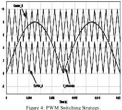
modulating signal is (Ar and the amplitude of each carrier is (Ac. In addition, each carrier is shifted with the carrier amplitude (Ac from the former one, as shown in Fig. 4.
Figure 4: PWM Switching Strategy.
IV. SWITCHING ALGORITHM FOR THE PROPOSED INVERTER USING PWM
The switching patterns employed in the proposed inverter are illustrated in Fig. 5. The output voltage levels, according to the switch ON/OFF conditions, are shown in Table II.
T ABLE II. OUTPUT VOLT AGE ACCORDING T O T HE SWIT CH ON/OFF CONDIT IONS
In this paper, the switching strategy used to generate the gate signals is accomplished by comparing the reference signal, which is rectified sinusoidal, with two triangular carrier waveforms having the same frequency and phase angle, but with different offset voltages. When the lower carrier signal is compared with the reference signal, the
first level of output voltage will be generated. This means that the modulation index (MI) is less than or equal 0.5 (50%). The behavior of proposed inverter is similar to the conventional full–bridge three-level PWM inverter. The distribution of the harmonic components in output voltage is similar to that of the conventional inverter having the values of two times the modulation index. The mentioned above is the first operational mode. On the other hand, if the required output voltage is increased beyond the modulation index 0.5, the output will result from comparing the upper carrier signal with the same reference signal. Therefore, the second level of the output voltage will be generated and it will be the second mode. According to the amplitude of the voltage reference, the operational interval of each mode varies within a certain period.
The modes are determined as the phase angle depends on the modulation index
(1) The modulation index ܯܯof the proposed five-level PWM inverter is defined as follows:
(2)
Where:
AM The peak value of the modulating (sinusoidal)
signal, i.e. the voltage reference (ferV) .
cAThe peak–to–peak value of the carrier (triangular).
Also, the frequency ratio, mf is defined as follows:
(3)
Where:
fc The frequency of the carrier (triangular) signal. fMThe frequency of the modulating (sinusoidal) signal.
When the modulation index is less than 0.5, the phase angle displacement is equal to:
(4) And when the modulation index is greater than 0.5, the phase angle displacement is
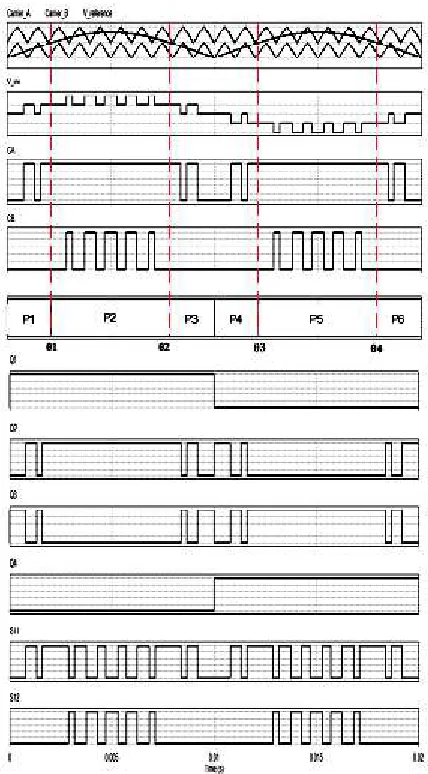
The switching Patterns of the proposed inverter is illustrated in Fig. 5. In one period, switches Q1and Q4operate at the fundamental frequency (i.e., 50 Hz). The switch S11 will be completely switched at the carrier signal frequency, whereas Q2and Q3will be switched in both low and high switching frequency. The switch S12 is switching at high frequency in a certain time of the period and off elsewhere. The output voltage according to the switch ON/OFF conditions is shown in Table II.
Figure 5: Switching Patterns of T he Proposed Inverter.
As shown in Fig. 5, the control signals are generated by the signals CA and CB, coming from the comparators, which compare the respective carrier signals with the voltage reference (Vref). The main six periods P1, P2, P3, P4, P5 and P6 can be calculated from the intersection of the reference waveform with the carrier signals. Then
switches signals Q1-Q4, S11-S12 can be formulated based on P1, P2, P3, P4, P5 and P6 by the phase angle displacement as given by equation (6).
.. (6)
V.MATLAB MODELING AND SIMULATION RESULTS
Here Simulation is carried out in different cases, in that 1). Proposed Single Phase Five Level Inverter with Grid Interconnection 2). Proposed Three Phase Five Level Inverter with Grid Interconnection.
Case 1: Proposed Single Phase Five Level Inverter with Grid Interconnection
Fig.6 Matlab/Simulink Model of Proposed Single Phase Five Level Inverter
Fig.7 Five Level Output Voltage
Fig.7 Five Level Output Voltage of Proposed Single Phase Five Level Inverter.
Fig.8 Matlab/Simulink Model of Proposed Single Phase Five Level Inverter with Grid Connection
Fig.8 shows the Matlab/Simulink Model of Proposed Single Phase Five Level Inverter with Grid Connection using Matlab/Simulink Platform.
Fig.9 Grid Voltage with Inverter Voltage
Case 2: Proposed Three Phase Five Level Inverter with Grid Interconnection
Fig.10 Matlab/Simulink Model of Proposed T hree Phase Five Level Inverter
Fig.10 shows the Matlab/Simulink Model of Proposed Single Three Five Level Inverter using Matlab/Simulink Platform.
Fig.11 T hree Phase Five Level Output Voltage
Fig.11 Three Phase Five Level Output Voltage of Proposed Three Phase Five Level Inverter.
VI.CONCLUSION
Multilevel inverters have received more attention in industrial applications, such as motor drives, static VAR compensators (STATCOMs) and renewable energy systems. Compared to the traditional two-level voltage source inverters, the stepwise output voltage is the major advantage of multilevel inverters. This paper has presented a new single-phase and three phase five-level PWM inverter with grid connection control. The proposed control technique for PWM switching and for the grid injected current control has been presented.. The major benefits of the proposed inverter are summarized as follow: It has less number of power elements. Some switches operate at fundament load frequency and others operate at carrier frequency. Smaller filter size, less circuit layout complexity and high efficiency can be achieved. Both the grid voltage and the grid current are in phase, so the system operates at unity power factor, and hence inject active power to the grid.
REFERENCES
[1] “Modern power electronics and ac drives” by bimal k bose.
[2] Muhammad H Rashid , “Power Electronics: circuits, Devices and Applications", Pearson Education, T hird Edition, 2004.
[3] J.S. Lai and F.Z. Peng, “Multilevel Converters - A new breed of power converters,” Conference Record of the IEEE-IAS Annual Meeting, 1995, pp. 2348-2356.
[5] Mohan M. Renge and Hiralal M. Suryawanshi, “Five-Level Diode clamped Inverter to eliminate Common Mode Voltage and Reduced dv/dt in Medium voltage rating Induction Motor Drives, IEEE Transactions on Power Electronics, vol. 23, no.4, pp. 1598–1607 July 2008.
[6] Mostafa Khazraei, Hossein Sepahvand, Keith A. Corzine, and Mehdi Ferdowsi, “Active Capacitor Voltage Balancing in Single-Phase Flying- Capacitor Multilevel Power Converters” IEEE Transactions on Industrial Electronics, VOL. 59, NO. 2, FEBRUARY 2012.
[7] Xu Lie, Jon C. Clare, Patrick W. Wheeler, Lee Empringham, and Li Yongdong, “Capacitor Clamped Multilevel Matrix Converter Space Vector Modulation” IEEE Transactions on industrial electronics, VOL. 59, NO. 1, JANUARY 2012.
[8] Fernanda Carnielutti, Humberto Pinheiro, and Cassiano Rech,
“Generalized Carrier-Based Modulation Strategy for Cascaded Multilevel Converters Operating Under Fault Conditions” IEEE