41 | P a g e
THEORETICAL STUDY OF SYMMETRICAL FOUR
QUANTUM WELL STRUCTURE USING TRANSFER
MATRIX METHOD
Md. Waesh Ali
1, Vishal Kumar
2, R. K. Lal
31,2,3
Electronics & Communication Engineering, Birla Institute of Technology, Mesra, Ranchi, (India)
ABSTRACT
In this paper a theoretic investigation of transmission coefficient for symmetrical structures of four-quantum
well (GaAs/AlxGa1−xAs) has been carried out using Transfer Matrix Method (TMM). The structures made of
quantum wells and barriers with different Al content both in the wells and barriers creating different energy
band diagram without applied bias. The result of change in Aluminum mole fraction in AlxGa1−xAs barrier
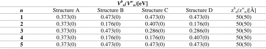
region has been incorporated through variable effective mass in the Schrödinger time independent equation. The performance of transmission coefficients has been studied for the structure by changing the barrier height gradually increasing and decreasing. The effect of energy E on Transmission coefficients considering tunneling effect is shown for four well structures using TMM in MATLAB.
Keywords- Transmission Coefficient, Transfer Matrix Method, MQW, symmetric, MATLAB
I INTRODUCTION
Currently, the buzzing word is the quantum confinement. Quantum effect that is planned to trap carriers within a very tiny space is known as quantum confinement. For definite use or research we need to change the electrical or optical property of a material and the efficient way to do so is the quantum confinement [1]. Some novel devices based on heterostructures of this kind of material have been reported by Rogalski [2].
Due to their diversity of technological usage, single and multiple semiconductor quantum-well structures have been widely studied in different situations [3] [4]. Based on mature III–V materials technology such as GaAs/AlGaAs structures, Quantum Well Infrared Photodetector (QWIP) structures have potential advantages promising high sensitivity, low power, low cost, high performance focal plane arrays and monolithic integration with high speed electronic devices [5].
42 | P a g e
Numerous approaches have been presented to solve the Schrodinger equation numerically. Two examples are the WKB approximation [7] and the variational calculations [8], [9]. Ghatak et al. [10]present a matrix method, for solving the Schrodinger equation in quantum-well structures, which in principle we have used here. In [11] the energy levels are found by the stabilization method of quantum chemistry. Furthermore, many methods associates with these difficulties are clumsy to implement. Two such examples are the Monte Carlo method [12] and the finite element method (FEM) [13], [14]. To implement algorithms based on these methods expert knowledge in computer science is required. The method used here, the TMM, is simple to implement and gives swift and exact answers to complex problems.In this paper, we present the theoretical study of some symmetrical four quantum well infrared photodetector structures, based on the GaAs/AlGaAs material system with adjustable Al concentrations in the quantum barriers. Transmission probability of four quantum well structure is numerically calculated using transfer matrix technique to find the possibility of resonant tunneling, and results are compared with each another structures which are similar type of structural parameters. Material composition of barrier layer are varied to witness the effect transmission for almost perfect result.
II THEORITICAL MODEL
To realize the physical properties of device structures, it is vital to simulate the expected performance on a computer. Here, we use Transfer Matrix Method for its simplicity and to provide a realistic precision. We have reviewed the variation of the effective mass and barrier height of AlGaAs barrier with aluminum concentration into the calculations.
The typical Schrodinger equation can be written for each of the semiconductor layers is as follows: 2
(z) (z) (z)
2 2
* 2 V
m z
E
in the AlGaAs barrier (1) 2
2 2
(z) (z) 2 *m z E
in the GaAs well (2)
Where, E is the energy of electron, in the well region conduction band potential is zero and effective mass of electron m∗equal to mwand in the barrier region conduction band potential is V and m∗is equal to mb.
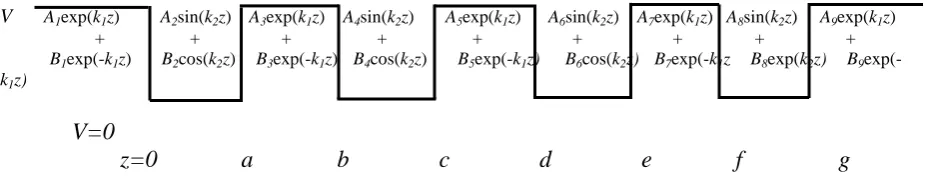
V
A1exp(k1z) A2sin(k2z) A3exp(k1z) A4sin(k2z) A5exp(k1z) A6sin(k2z) A7exp(k1z) A8sin(k2z) A9exp(k1z)
+ + + + + + + + +
B1exp(-k1z) B2cos(k2z) B3exp(-k1z) B4cos(k2z) B5exp(-k1z) B6cos(k2z) B7exp(-k1z B8exp(k2z) B9
exp(-k1z)
V=0
z=0 a b c d e f g
43 | P a g e
The energy E must be less than barrier height V, for the proper confinement of the electrons in the well. The Multiple Quantum Well (MQW) structures considered for the theoretic investigation for 4 wells is as shown in Fig. 1. The general solutions of the Schrodinger equation for this MQW structure in every region are as follows:
(z) A exp k z1 1 B exp1 k z1
,
z<0 (3)
(z) A sin k z2 ( 2 ) B cos k z2 2
, 0<z<a (4)
(z) A exp k z3 1 B exp3 k z1
, a<z<b (5)
(z) A sin k z4 ( 2 ) B cos k z4 2
, b<z< c (6)
(z) A exp k z5 1 B exp5 k z1
, c<z< d (7)
(z) A sin k z6 ( 2 ) B cos k z6 2
, d<z< e (8)
(z) A exp k z7 1 B exp7 k z1
,
e<z< f (9)
(z) )
2 (
8 8 2
A sin k z B cos k z
, f<z< g (10)
(z) A exp k z9 1 B exp9 k z1
, g<z (11)Where,
( 1
2m*b V )
k
E
&
2 2
* m
k wE
After choosing all the wells to be of the same depth, and all the barriers to be of the same height V, we can simplify that the wave vectors in quantum well and barrier region, k1 & k2 are constant all over the structure.
Proceeding with continuity of wave function and its first derivative divided by the effective mass at the each interface of well and barrier region for 4 well structure as follows:
Considering z=0 first, we have
1 1 2
A B B (12)
1 1
( 1 1 1 1) 1 2
* k A k B * A
m m w
k b
(13)
Similarly, with z=a,
)
2 ( 2 2 2 3 1 3 1
A sin k a B cos k a A exp k a B exp k a (14)
( ]
1 1
[ 2 2 2 ) 2 2 2 [ 1 3 1 3 1
* k A s k a k B in k a * k A exp k a B exp k a ]
m
co
m b
s w
(15)
Proceeding with z=b,
)
3 1 3 1 4 ( 2 4 2
44 | P a g e
1 1
[ 1 3 1 1 3 1 [ 2 2 ) 2 2
* k A exp k b k B exp k b ] * k A4 s k b( k B sin k b4 ]
m m b co w
(17)
With z=c,
)
2 2
( 5 5
4 4 1 1
A sin k c B cos k c A exp k c B exp k c (18)
( ]
1 1
[ 2 2 ) 2 2 [ 1 1 1
* k A4 s k c k B4 in k c * k A exp k c5 B exp5 k c ]
m co m b s w
(19)
With z=d,
1
1 ( 2 )
25 5 6 6
A exp k d B exp k d A sin k d B cos k d (20)
1 1
[ 1 5 1 1 5 1 ] [ 2 6 ( 2 ) 2 6 2 ]
* k A exp k d k B exp k d * k A s k d k B sin k d
m b m
co w
(21)
With z=e,
)
2 2
( 7 7
6 6 1 1
A sin k e B cos k e A exp k e B exp k e (22)
( ]
1 1
[ 2 2 ) 2 2 [ 1 1 1
* k A6 s k e k B6 in k e * k A exp k e7 B exp7 k e ]
m co m b s w
(23)
With z= f,
1
1 ( 2 )
27 7 8 8
A exp k f B exp k f A sin k f B cos k f (24)
1 1
[ 1 7 1 1 7 1 ] [ 2 8 ( 2 ) 2 8 2 ]
* k A exp k f k B exp k f * k A s k f k B sin k f
m b m
co w
(25)
With z= g,
)
2 2
(
8 8 9 1 9 1
A sin k g B cos k g A exp k g B exp k g (26)
( ]
1 1
[ 2 2 ) 2 2 [ 1 1 1
* k A8 s k g k B in k g8 * k A exp k g9 B exp9 k g ]
m co m b s w
(27)
Which can be rewritten more neatly in matrix form as:
1 1 0 1
2
1 1 1
1 1
* * *
1
1 2 0 2
A A
k k B k B
m b m b m w
(28)
( 3 2) 1 1
2 2
) * 1 * 1
2 2 2
1 1
1 1
( 1
* 2 1
* 2 3
exp k a exp k a sin k a cos k a
A A
k exp k a k exp k a
B B
k cos k a k sin k a
m m
m w m w b b
45 | P a g e
( 3 41 1 1 1
( )
1 1 2 2
)
1 1
* 1 * 1 3 * 2 2 * 2 2 4
exp k b exp k b sin k b cos k b
A A
k exp k b k exp k b B k cos k b k sin k b B
m b mb m w m w
(30)
) 1 1
2 2
) * 1 * 1
2 2 ( 5 4 1 2 2 1 1 1
( 1 1 5
* * 4
exp k c exp k c sin k c cos k c
A A
k exp k c k exp k c
B B
k cos k c k s
w w b
i
m
m m b
n k c
m
(31)
( 5 61 1 1 1
( )
1 1 2 2
)
1 1
* 1 * 1 5 * 2 2 * 2 2 6
exp k d exp k d sin k d cos k d
A A
k exp k d k exp k d B k cos k d k sin k d B
m b mb m w m w
(32)
) 1 1
2 2
) * 1 * 1
2 2
(
6 1 7
2 2
1
1 1
( 6 1 1 7
* *
exp k e exp k e sin k e cos k e
A A
k exp k e k exp k e
B B
k cos k e k s
w w b
i
m
m m b
n k e
m
(33)
( 7 81 1 1 1
( )
1 1 2 2
)
1 1
* 1 * 1 7 * 2 2 * 2 2 8
exp k f exp k f sin k f cos k f
A A
k exp k f k exp k f B k cos k f k sin k f B
m b mb m w m w
(34)
) 1 1
2 2
) * 1 * 1
2 2
(
8 1 9
2 2
1
1 1
( 8 1 1 9
* *
exp k g exp k g sin k g cos k g
A A
k exp k g k exp k g
B B
k cos k g k s
w w b
i
m
m m b
n k g
m
(35)Labelling the 2⨯2 matrix for the left-hand side of the nth interface as M2n-1 and the corresponding matrix for the
right hand side of the interface as M2n, n=1, 2, 3, etc., then the above matrix equations would become:
2 1 2 2 1 1 A A M M
B B
(36)3 2 3 4 2 3 A A M M
B B
(37)3 4
5 6
3 4
A A
M M
B B
(38)5 4 7 8 5 4 A A M M
B B
(39)5 6 9 10 5 6 A A M M
B B
46 | P a g e
6 7 11 12 7 6 A A M MB B
(41)7 8 13 14 7 8 A A M M
B B
(42)8 9
15 16
8 9
A A
M M
B B
(43)Now Eq. (36) gives:
2 1 2 1 2 1 1 A A M M B B
(44)and Eq. (37) gives:
3 2 3 2 3 1 4 A A M M B B
(45)therefore
3
1 2 3
1 1
1
1 4 3
A A
M M M M
B B
(46)and eventually
1 1 1 1 1 9
5 7
1 2 3 4 6 8 9 1
1
0 11 12 13 14
1 1
1
15 1
1 6 9
A A
M M M M M M M M M M M M M M M M
B B
(47)The product of the sixteen 2⨯2 matrices is still a 2⨯2 matrix; thus writing
9
1 9
1
A A
B B
M
(48)then
9
1 9
A M11A M12B (49)
9
1 9
B M21A M22B (50)
To know the exact solution of the wave function we have to apply normalization condition which determines the unknown coefficients An and Bn in above equations. The probability interpretation of the wave function implies
that the wave function must tend towards zero at the outer barriers, i.e. the coefficients of the growing exponentials must be zero. In this case, with the origin at the 1st interface (see Fig. 1), then this implies that
1
B =0 and 9
A =0, and hence the second of the above equation would imply that
M22
=0. As all of the elements ofM
are function of1
k and 2
k , which are both in turn functions of the energy E, then an energy is sought which satisfies the following condition:
( )
E
0
2247 | P a g e
Once the energy is known through the standard numerical procedures, the coefficientsA
1 toB
9follow simply and the envelope wave function has been deduced. Multiplying matrices together for the entire potential shape, the wave functions, and confined energies are calculated for the entire system. For systems where the states are not bound and properly confined, TMM can be used to calculate the transmission coefficients as
*1
T E
11 11
M M
(52)At this situation,
M
11 defines first matrix element, which is taken from matrixM
andM
11*defines conjugate form ofM
11 .The reason behind using the Transfer Matrix Method is to get the electron energy precisely and to investigate the transmission coefficients alongside. The transmission coefficient is essential to examine the tunneling of the electron through the quantum well. The transmission coefficient has been a significant quantity as it delivers most of the relevant information of the transport process in MQW [6] [15].
III DEVICE STRUCTURE
The device structures, which we study, is a four-well system, comprising of GaAs/AlxGa1−xAs quantum wells
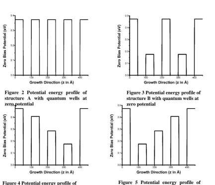
and barriers named as structure A, structure B, structure C and structure D where mole fraction, x, varies from 0 to 0.43 and for the wells the mole fraction is constant at zero. The exact composition of all quantum barriers are given in Table 1. The consecutive device potentials (V) are given in Table 2. Here, zbn (znw) shows the distance
of the left hand side of the nth barrier (well) from origin [16]. The different structures from A to F which are designed and studied has been shown from Fig. 2 to Fig. 5 respectively.
Table 1: Summary of composition used in the different structures
Composition for Al (x)
Structure A Structure B Structure C Structure D
First Barrier 33.9 0.43 0.43 0.43
Second Barrier 33.9 0.16 0.37 0.16
Third Barrier 33.9 0.43 0.26 0.26
Fourth Barrier 33.9 0.16 0.16 0.37
Fifth Barrier 33.9 0.43 0.43 0.43
Table 2: Summary of calculated potential & thickness designed in the different structures
Vbn(V w
n)[eV]
n Structure A Structure B Structure C Structure D zbn(zwn)[Å]
1 0.373(0) 0.473(0) 0.473(0) 0.473(0) 50(50)
2 0.373(0) 0.176(0) 0.407(0) 0.176(0) 50(50)
3 0.373(0) 0.473(0) 0.286(0) 0.286(0) 50(50)
4 0.373(0) 0.176(0) 0.176(0) 0.407(0) 50(50)
48 | P a g e
IV RESULTS & DISCUSSION
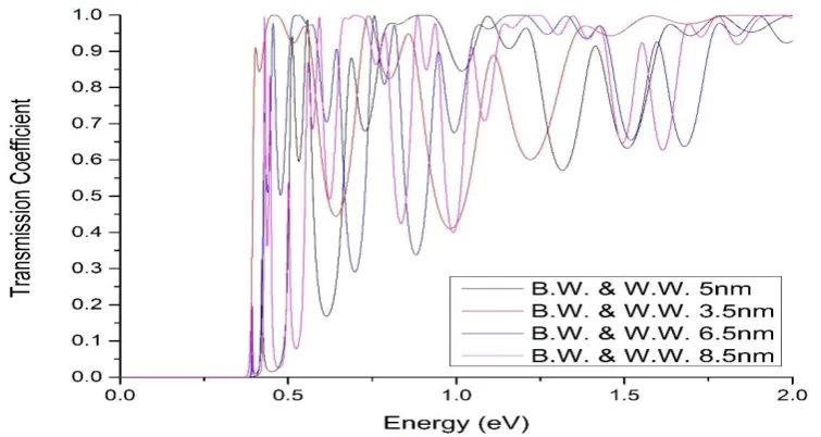
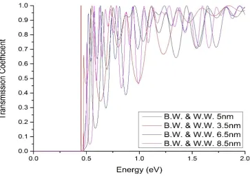
We have investigated thorough analysis of MQW (for n=4) structures in which well width and barrier width is of the order of nanometers. By using Eq.(53), the transmission coefficient of different symmetrical structures is computed for all the geometries when electric field is absent. The structure investigation for computation of resonant transmission probability is achieved by varying dimensional formation such as different well width (W.W.) and barrier width (B.W.) of 3.5nm, 5nm, 6.5nm and 8.5nm for all the symmetrical structures.
It is also taken care that barrier potential is exclusively a function of the material parameters, and effective masses of barrier section and in well section have a mismatch as it depends on composition of Al in barrier sections. The result for structure A to D is shown in Fig. 6 to Fig 9 respectively.
Fig. 6 gives the profile of transmission coefficient for structure A as function of energy for different well widths and barrier widths of the structure are considered identical and kept unchanged for the simulation purpose. For that structure, with increasing well width, tunneling probabilities can be estimated at lower energy values. In Fig. 7 we see that the tunneling probability becomes better in structure B in comparison to structure A as the transmission reaches near unity in lower energy. Due to the lower well width and barrier width, the structure A
Figure 2 Potential energy profile of structure A with quantum wells at zero potential
Figure 3 Potential energy profile of structure B with quantum wells at zero potential
Figure 4 Potential energy profile of structure C with quantum wells at zero potential
49 | P a g e
has subband at lower energies. As, in structure A the well depth is greater the notches in the transmission probability becomes sharper. But in the structure B, well depth is not consistent and much less than in structure A, so the tunneling probability fluctuation is fewer and it achieves more transmission at lower energies.For the case of structure C & D, in Fig. 8 & 9, in both geometrics we see that, as the 2nd, 3rd and 4th barrier potential is lower than the 1st and 5th barrier, the lowest well width and barrier width provides maximum transmission probability at very low energy. But it takes more energy in structure D due to the increased barrier height in later stage of growth direction.
Figure 6 Comparative profile of transmission coefficients as a function of energy for different
B.W. & W.W. for structure A in absence of electric field
Figure 7 Comparative profile of transmission coefficients as a function of energy for different B.W. &
50 | P a g e
Figure 8 Comparative profile of transmission coefficients as a function of energy for different B.W. &
W.W. for structure C in absence of electric field
Figure 9 Comparative profile of transmission coefficients as a function of energy for different B.W. &
51 | P a g e
V CONCLUSION
The simulation is done using MATLAB. Effect of different well width & barrier width is designed and analyzed theoretically on transmission coefficient in symmetrical 4-quantum well device with barrier potential variation. We can conclude that transmission coefficient is better obtained for the lowest well & barrier width structure due to the higher tunneling probability at lower energies.
This investigation delivers the significant results to examine the behavior of complex quantum well structures, providing its applicability to define quantum confinement in multiple quantum well structures and will provide the information when the parameters are varied of the designs.
REFERENCES
1. Khan, "Analysis of a Finite Quantum Well," Journal of Electrical Engineering, vol. 37, no. 2, pp. 10--14, 2012.
2. A. Rogalski, "Heterostructure infrared photovoltaic detectors," Infrared Physics & Technology, vol. 41, no. 4, pp. 213--238, 2000.
3. E. Ozturk and I. Sokmen, "Intersubband transitions in an asymmetric double quantum well," Superlattices
and Microstructures, vol. 41, no. 1, pp. 36--43, 2007.
4. K. Mukherjee and N. Das, "Tunneling current calculations for nonuniform and asymmetric multiple quantum well structures," Journal of Applied Physics, vol. 109, no. 5, p. 053708, 2011
5. F. F. Sizov and A. Rogalski, "Semiconductor superlattices and quantum wells for infrared optoelectronics,"
Progress in quantum electronics, vol. 17, no. 2, pp. 93--164, 1993.
6. K. Talele and D. S. Patil, "Analysis of wave function, energy and transmission coefficients in GaN/ALGaN superlattice nanostructures," Progress In Electromagnetics Research, vol. 81, pp. 237--252, 2008.
7. R. Spigler and M. Vianello, "A survey on the Liouville-Green WKB approximation for linear difference equations of the second order," Advances in Difference Equations (Veszprém, 1995), pp. 567--577, 1995. 8. G. Bastard, E. Mendez, L. Chang and L. Esaki, "Variational calculations on a quantum well in an electric
field," Physical Review B, vol. 28, no. 6, p. 3241, 1983
9. D. Ahn and S. Chuang, "Variational calculations of subbands in a quantum well with uniform electric field: Gram--Schmidt orthogonalization approach," Applied physics letters, vol. 49, no. 21, pp. 1450--1452, 1986. 10. A. K. Ghatak, K. Thyagarajan and M. Shenoy, "A novel numerical technique for solving the one-dimensional Schroedinger equation using matrix approach-application to quantum well structures," IEEE
Journal of Quantum Electronics, vol. 24, no. 8, pp. 1524--1531, 1988[11]
11. F. Borondo and J. Sanchez-Dehesa, "Electronic structure of a GaAs quantum well in an electric field,"
Physical Review B, vol. 33, no. 12, p. 8758, 1986
12. J. Singh, "A new method for solving the ground-state problem in arbitrary quantum wells: Application to electron-hole quasi-bound levels in quantum wells under high electric field," Applied physics letters, vol.
48, no. 6, pp. 434--436, 1986.
52 | P a g e
14. K. Nakamura, A. Shimizu, M. Koshiba and K. Hayata, "Finite-element analysis of quantum wells ofarbitrary semiconductors with arbitrary potential profiles," IEEE Journal of Quantum Electronics, vol. 25,
no. 5, pp. 889--895, 1989.
15. P. Harrison, Quantum wells, wires and dots: theoretical and computational physics of semiconductor nanostructures, 2nd ed., TJ International, Padstow, Cornwall, Great Britain: John Wiley & Sons, 2005. 16. S. Eker, M. Hostut, Y. Ergun and I. Sokmen, "A new approach to quantum well infrared photodetectors: