Design and Implementation of Programmable
Logic Controller (PLC) Using System on
Programmable Chip (SOPC)
Vilas V Deotare1, Arjun J. Khetia2, Dinesh V Padole3
Professor, Dept. of Electronics and Telecommunication, GHRCE, Nagpur, Maharashtra, India1
Research Scholar, Dept. of Electronics and Telecommunication, GHRCE, Nagpur, Maharashtra, India2,3
ABSTRACT: Programmable logic controller (PLC) is one of the most important components in today’s manufacturing. Its performance-based microprocessor and software have been a bottleneck for improving its efficiency. To enhance the PLC performance and flexibility, a new PLC design based on field programmable gate array (FPGA) has been a hot topic because of its parallel execution mechanism and reconfigurable hardware structure. From practical viewpoint, in this paper, the authors propose an approach to implement the existing ladder diagram (LD) inside FPGA making full use of the advantage of FPGA device. The design also provides the GUI (Graphical User Interface) connectivity based controlling of designed PLC for the ease of monitoring and controlling the PLC and its applications from the control center. We can easily monitor and control different devices from Personal Computer (PCs). This discusses the implementation of FPGA based PLC that can be embedded into devices, machines & systems using suitable interface for industrial applications as well as for home applications. It provides Real-Time Speedy Operations and FPGA based Real-Time Control Systems with a capability to run multiple control tasks for reliable developing, monitoring and controlling of systems. The design results into highly cost-effective, compact and simple solution.
KEYWORDS: Programmable Logic Controller (PLC), Automation, Very Large Scale Integration System (VLSI), System on Programmable Chip (SOPC).
I. INTRODUCTION
Programmable logic controllers (PLCs) have been widely used for the logic control in the manufacturing system [1]. In industrial application, ladder diagram is the most popular programming language for PLC development. Traditionally, PLC includes a microprocessor, and the ladder diagram is sequentially executed inside this PLC microprocessor in a cyclic scan period. Based on this solution, PLC performance is limited by the cyclic scan period, which depends on the program length and the microprocessor’s processing speed. In order to overcome these drawbacks with the programmable hardware solution, field programmable gate array (FPGA)-based PLC has been focused on by many researchers with its reconfigurable hardware structure and parallel execution advantage. Miyazawa [2] and Ikeshita et al. [3] developed a very rough manner in 1999 to convert the graphic ladder diagram into program description of very high-speed integrated circuit hardware description language (VHDL). Chen and Patyra [4] designed a VHDL model of the whole system directly from the original system requirements to build a controller. Abdel-Hamid et al. [5] and Kuusilinna et al. [6] developed an algorithm to convert finite state machine (FSM) into VHDL.
In FPGA design, parallel execution exists not only in one combinational logic operation but also in the multiple combinational logic operations. To the first case, in one combinational logic operation, there is only one output. But, all of the combinational logics which influence this output have been designed in a flat way as the existing circuit. The operation can be executed at the electrical speed. To the second case, in the multiple combinational logic operations, all of these combinational logic operations that influence every output have been designed in a flat way as the existing circuits. So they can occur in a parallel way. For the first case, it is very easy to be realized in VHDL. In this paper, the parallel execution to be discussed here specially means the second case.
PLC instructions have been considered and designed with circuit, which can be activated by sensitive signals. In order to implement PLC ladder diagram inside FPGA, the sequential operations in the original ladder diagram should be kept. At the same time, the capability of parallel execution can be used to get more efficient performance. This paper will discuss how to implement the PLC ladder diagram in the sequential execution way and the parallel execution way inside FPGA. Programming language for FPGA is VHDL.
In FPGA design, parallel execution exists not only in one combinational logic operation but also in the multiple combinational logic operations. The design also provides the GUI (Graphical User Interface) based controlling of designed PLC for the ease of controlling the PLC and its applications from the control room also. We can easily monitor and control different devices from Personal Computer (PCs).
II. FPGA-BASEDPLCDESIGN
A. Hardware framework
The hardware framework of FPGA-based PLC is shown in Figure 1. This framework includes FPGA chip, I/O unit, A/D module, reset circuit, power supply circuit, program memory chip EPCS4, JTAC download port etc. ISA interface is used for communication with host computer, I/O unit and A/D module are used for acquisition of digital and analog signals.
Fig.1.FPGA-based PLC Hardware Framework
B. Software Framework
The This VHDL consists of two modules: One is ISA communication decoding module, which packages address decoding and latches data into the interface package. The other is generation module of VHDL program that has equivalent function with the ladder diagram. The difficult and key technology is how to convert the ladder diagram into VHDL.
The Hardware/Software co-design Technology results in better solution providing following advantages:
2) Accuracy: Design being fast enables engineers to incorporate extremely time-critical functions to hardware such as limit and proximity sensor detection and sensor health monitoring resulting in more accurate solutions. 3) Short product development cycle: Due to the use of standard HDLs and automated design tools design time is
much reduced. Also the control code runs directly in silicon, engineers can try out various implementations. 4) Cost effective and compactness: Due to above advantages designer can meet the market requirements by
satisfying customer needs, increase the performance or functionality of the product. Hence result in high performance, low cost and compact designs as compared to the other available solutions.
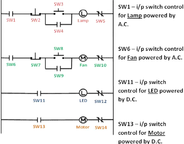
C. Relay Ladder Logic
Relay ladder logic emulates a synchronous electromechanical relay panel. It pictures control logic as a one-way flow from a left rail of the ladder across its rungs toward coil elements along the right rail. Flow along a rung is passed or cut off by a series of relays (contacts), effectively defining logical products. Vertical paths between rungs allow flows to merge, effectively summing the rung products. All ladder logic dialects describe this same basic form.
Figure 2 illustrates the graphical symbols used in programming relay ladder logic. Contacts are of two kinds. A normally open contact passes the flow when activated (i.e., closed), effectively inserting its variable into a product term. A normally closed contact passes the flow unless activated (i.e., opened), effectively inserting the complemented variable into the product. Coils are state variables.A set of adjacent rungs connected by vertical paths is called a network. On each cycle of operation, known as a scan, the flow for all networks is computed. Flow on an individual network implements a Boolean function for one state or output variable.
Fig.2.Relay Ladder Logic Diagram
III.IMPLEMENTATION OF FPGA-BASED PLC
functions as the original PLC ladder diagram, but not in the traditional sequential cyclic scan manner. The new solution can respond to the input signals with parallel execution at hardware processing speed, which dramatically improve the PLC speed. Moreover, it can be reconfigured any times as a new PLC program is converted and downloaded.
IV.LADDER DIAGRAM PROGRAM
The PLC performs its execution cyclically. It reads input status, executes logic and updates output status. It is called as a PLC scan. Scanning of ladder program occurs from left to right and top to bottom repeatedly. Scanning of complete ladder program is ladder scan cycle.
There are two modes of operating a PLC
1) Program Mode: In this mode, the ladder program is loaded into the program memory of PLC. 2) Run/Execution: In this mode, the PLC executes the ladder logic cyclically.
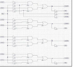
Figure 3 shows the translated circuit of PLC which can program on any FPGA with the help of Xilinx and controlled with user controlled software from personal computer.
Fig.3.Design Architecture of PLC translated circuit
V. DESIGN CONSIDERATIONS
1) Size:Size of the design increases with increase in number of instructions/functions, which a PLC can handle, number of rungs that can be connected in parallel (p). Hence designer can use an instruction set containing optimum instructions.
3) Memory: PLC requires memory to store program and temporary data. In conventional PLCs separate memory chips are used for this purpose. With the proposed design one can use the memory available inside same FPGA chip reducing extra circuitry and delays involved in read/write operations in conventional designs. This results in a faster and compact solution. The demonstrated design used block memory as user memory and distributed memory as data memory. Furthermore extra huge memory is available with hardware – software co-design by using the system’s memory to store and read data from ROM of computer.
VI.SOFTWARE (GUI)
Field Programmable Gate Array (FPGA) based Programmable Logic Controller (PLC) GUI is developed by using Visual Studio 2010 software in VB.Net language with serial (RS232) as USB connectivity. As shown in figure 4 the GUI (Graphical User Interface) screen, with monitoring as well as controlling and timer configuration module is also shown.
Fig.4.Software GUI Screen
VII. DESIGN TESTING AND RESULTS
Fig.5.Simulation Waveforms of the Ladder Logic Functionality
Theresults of simulation verify that the converted VHDL program can perform the same function as the ladder diagram does. Synthesize this VHDL program and download it to the FPGA, the control system will be implemented inside FPGA.
VIII. CONCLUSION
In order to overcome the performance limitation of the traditional microprocessor-based PLC and dramatically improve the PLC performance, in this paper, FPGA-based PLC is proposed. The idea has been implemented and demonstrated at smaller scale for typical application. Also the design is limited to digital I/O channels, it can be further extended for Analog I/O channels.
Furthermore, as a programmable hardware solution, FPGA device is reconfigurable, which make it easier for the application system to be modified and maintained. The design method is more flexible. From a practical viewpoint, this research is still in a nascent stage of development. There are several mathematical issues that must be examined. With the rapidly increasing extension of instruction of the LD program and increasing requirements of PLC, much more research needs to be done to improve this work.
ACKNOWLEDGMENT
The authors would like to acknowledge their gratitude and vote of thanks to all the faculty members of Sinhgad Institute of Technology, especially to the Head of Department of Electronics and Telecommunication for providing the needed help and motivation. Also to their parents and friends for providing co-operation, necessary resources and support forever.
REFERENCES
2. Zhu Huabing*, Liang Benlei, Dong Bolin, Feng Xiao, “Research on FPGA-based Programmable Logic Controllers’ Technology”, December 2013 Telkomnika.
3. C. Economakos and G. Economakos, “FPGA Implementation of PLC Programs Using Automated High-Level Synthesis Tools”, IEEE International Symposium on Industrial Electronics (ISIE 08), 2011, pp. 1908-1913.
4. C. Economakos and G. Economakos, “Optimized FPGA Implementations of Demanding PLC Programs Based on Hardware High-Level Synthesis”, 13th IEEE International Conference on Emarging Technologies and Factory Automation (ETFA ’08), 2011, pp. 1002-1009. 5. Daoshan Du &XiaodongXu& Kazuo Yamazaki, “A study on the generation of silicon-based hardware Plc by means of the direct conversion of
the ladder diagram to circuit design language”, May 2010 Springer.
6. DhanashriGawali&V.K.Sharma, “FPGA BASED MICRO-PLC DESIGN APPROACH”, 2009 IEEE.
7. Daoshan Du &Yadong Liu &XinguiGuo& Kazuo Yamazaki & Makoto Fujishima, “Study on LD-VHDL conversion for FPGA-based PLC implementation”, 2009 Springer.
8. S. Ichikawa, M. Akinaka, R. Ikeda, H. Yamamoto, “Converting PLC Instruction Sequence into Logic Circuit: a Preliminary Study”, IEEE International Symposium on Industrial Electronics (ISIE 2006), 2009, pp. 2930-2935