Theses & Dissertations Boston University Theses & Dissertations
2015
Designing energy-efficient
sub-threshold logic circuits using
equalization and non-volatile
memory circuits using memristors
https://hdl.handle.net/2144/16096COLLEGE OF ENGINEERING
Dissertation
DESIGNING ENERGY-EFFICIENT SUB-THRESHOLD
LOGIC CIRCUITS USING EQUALIZATION AND
NON-VOLATILE MEMORY CIRCUITS USING
MEMRISTORS
by
MAHMOUD ZANGENEH
B.S., Amirkabir University of Technology (Tehran Polytechnic), 2007
M.S., University of Tehran, 2010
Submitted in partial fulfillment of the
requirements for the degree of
Doctor of Philosophy
2015
First Reader
Ajay Joshi, PhD
Assistant Professor of Electrical and Computer Engineering
Second Reader
Allyn Hubbard, PhD
Professor of Biomedical Engineering
Professor of Electrical and Computer Engineering
Third Reader
Bennett Goldberg, PhD Professor of Physics
Professor of Biomedical Engineering
Fourth Reader
M. Selim ¨Unl¨u, PhD
Professor of Biomedical Engineering
I would like to express my deepest appreciation to the committee members for re-viewing this dissertation and providing me precious feedback. Then I want to thank my adviser, Prof. Ajay Joshi, who led my research and worked with me for many interesting research topics. Also it is my pleasure to work with Zafar Takhirov in our group, who provided many experimental results and valuable suggestions. I want to thank members in our group Schuyler Eldridge, Boyou Zhou, and Chao Chen for making our research in the lab enjoyable.
Also I wish to thank Prof. Selim ¨Unl¨u and Prof. Bennett Goldberg for their sugges-tions in my research. They helped me overcome many technical obstacles when we were writing papers together. I also want to thank several members in their groups, including Dr. Ronen Adato, Dr. Berkin Cilingiroglu, Aydan Uyar, and Dr. Ab-dulkadir Yurt for all their contributions when we were working on research projects together.
In addition, a thank you to thank Prof. Ronald Knepper, Dr. David Freedman, Prof. Michelle Sander and Prof. Min-Chang Lee. I worked as a teaching fellow for their classes at Boston University. I enjoyed when helping undergraduate students with their homework and lab projects, and I also obtained a lot of useful knowledge for my later research.
Finally, I want to thank my father, Majid Zangeneh, my mother, Zarin Aghai Rashti and my brother, Masoud Zangeneh for their continuous support and encouragement. They helped me focus on the research and work hard for achieving my education and career goals. I hope to provide my parents better lives after graduation and spend more time with them.
LOGIC CIRCUITS USING EQUALIZATION AND
NON-VOLATILE MEMORY CIRCUITS USING
MEMRISTORS
MAHMOUD ZANGENEH
Boston University, College of Engineering, 2015
Major Professor: Ajay Joshi, PhD, Assistant Professor of
Elec-trical and Computer Engineering
ABSTRACT
The very large scale integration (VLSI) community has utilized aggressive comple-mentary metal-oxide semiconductor (CMOS) technology scaling to meet the ever-increasing performance requirements of computing systems. However, as we enter the nanoscale regime, the prevalent process variation effects degrade the CMOS device reliability. Hence, it is increasingly essential to explore emerging technologies which are compatible with the conventional CMOS process for designing highly-dense mem-ory/logic circuits. Memristor technology is being explored as a potential candidate in designing non-volatile memory arrays and logic circuits with high density, low latency and small energy consumption. In this thesis, we present the detailed functionality of multi-bit 1-Transistor 1-memRistor (1T1R) cell-based memory arrays. We present the performance and energy models for an individual 1T1R memory cell and the mem-ory array as a whole. We have considered T iO2- and Hf Ox-based memristors, and
for these technologies there is a sub-10% difference between energy and performance
write energy (4.06 pJ/bit) and read energy (188 fJ/bit) when storing 3 bits/cell for 100 nsec write and 1 nsec read access times. Similarly,Hf Ox-based RRAM array
con-sumes the least write energy (365 fJ/bit) and read energy (173 fJ/bit) when storing 3 bits/cell for 1 nsec write and 200 nsec read access times.
On the logic side, we investigate the use of equalization techniques to improve the energy efficiency of digital sequential logic circuits in sub-threshold regime. We first propose the use of a variable threshold feedback equalizer circuit with combinational logic blocks to mitigate the timing errors in digital logic designed in sub-threshold regime. This mitigation of timing errors can be leveraged to reduce the dominant leakage energy by scaling supply voltage or decreasing the propagation delay. At the fixed supply voltage, we can decrease the propagation delay of the critical path in a combinational logic block using equalizer circuits and, correspondingly decrease the leakage energy consumption. For a 8-bit carry lookahead adder designed in UMC 130 nm process, the operating frequency can be increased by 22.87% (on average), while reducing the leakage energy by 22.6% (on average) in the sub-threshold regime. Overall, the feedback equalization technique provides up to 35.4% lower energy-delay product compared to the conventional non-equalized logic. We also propose a tunable adaptive feedback equalizer circuit that can be used with sequential digital logic to mitigate the process variation effects and reduce the dominant leakage energy component in sub-threshold digital logic circuits. For a 64-bit adder designed in 130 nm our proposed approach can reduce the normalized delay variation of the critical path delay from 16.1% to 11.4% while reducing the energy-delay product by 25.83% at minimum energy supply voltage. In addition, we present detailed energy-performance models of the adaptive feedback equalizer circuit. This work serves as
threshold regime.
1 Introduction 1
1.1 Background and Motivation . . . 1
1.2 Contribution and Organization . . . 6
2 Memristor Technology and Modeling 10 2.1 Introduction . . . 10
2.2 Memristor Device Technology . . . 10
2.3 Summary . . . 18
3 Design of Multi-bit RRAM Array 19 3.1 Introduction . . . 19
3.2 Related Work . . . 19
3.3 RRAM Cell Design . . . 21
3.4 RRAM Array Architecture . . . 23
3.5 Performance Models . . . 25
3.6 Energy Models . . . 36
3.7 Memory Technology Comparison . . . 43
3.8 PVT Variation Analysis of n-bit RRAM Cell . . . 45
3.9 Summary . . . 53
4 Sub-threshold Logic Design using Feedback Equalization 55 4.1 Introduction . . . 55
4.2 Related Work . . . 56
4.4 Experimental Results . . . 63
4.4.1 Performance improvement at the fixed supply voltage . . . 64
4.4.2 Leakage reduction at the fixed operating frequency . . . 67
4.4.3 Mitigating process variations . . . 68
4.5 Effect of Technology Scaling . . . 69
4.6 Summary . . . 71
5 Tunable Sub-threshold Logic Circuits using Adaptive Feedback Equal-ization 72 5.1 Introduction . . . 72
5.2 Adaptive Equalized Flip flop versus Conventional Flip flop . . . 72
5.3 Modeling of Feedback Equalizer Circuits . . . 81
5.4 Evaluation . . . 90
5.4.1 Improvement of Energy Efficiency . . . 91
5.4.2 Maintaining Robustness Using Post-Fabrication Tuning . . . . 96
5.4.3 Mitigating Voltage/Temperature Variations . . . 99
5.4.4 Effect of Technology Scaling . . . 101
5.4.5 Comparison with other Sub-threshold Design Techniques . . . 103
5.4.6 Memristor-based Feedback Equalization Technique . . . 103
5.5 Summary . . . 105
6 Conclusion and Future Work 106 6.1 Conclusion . . . 106
6.2 Future Work . . . 109
6.2.1 Equalized Flip Flop with Bypass . . . 109
6.2.2 Equalization Techniques for Near-threshold Voltage Computing Applications . . . 110
References 114
Curriculum Vitae 122
1.1 Comparison between current emerging nonvolatile memory technologies. 4 2.1 Parameters of T iO2-based (Strukov et al., 2008) and Hf Ox-based
(Ielmini, 2011), (Sheu et al., 2009) memristors used for modeling and simulations. . . 13 3.1 Comparison between the reference voltages determined using analytical
model (AM) and HSPICE simulation (HS) for a readsub access time of
TR(T iO2) = 1, 2nsecin the 2-bit/cell 1T1R RRAM.VLL(T iO2) = 0.48 V is chosen to reach to at least 25 mV difference between the two adjacent reference voltages. The average error is 5.7% forT iO2. . . . 27
3.2 Comparison between the reference voltages determined using analyt-ical model (AM) and HSPICE simulation (HS) for a readsub access
time of TR(Hf Ox) = 200, 400 nsec in the 2-bit/cell 1T1R RRAM.
VLL(Hf Ox) = 0.7V is chosen to reach to at least 25 mV difference
be-tween the two adjacent reference voltages. The average error is 0.151% for Hf Ox. . . 27
3.3 Comparison between analytical model (AM) and HSPICE simulations (HS) for energy dissipated in the cell while reading 2-bit RRAM cell with a read access time ofTR(T iO2) = 1nsecandTR(Hf Ox) = 200nsec.
The average error is 8.44% and 0.038% forT iO2 andHf Ox respectively. 37
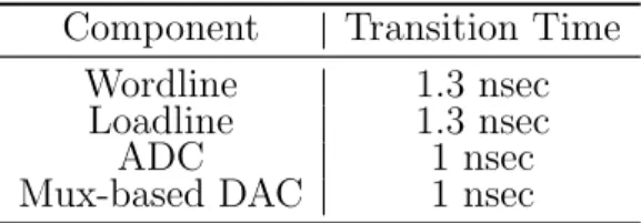
3.4 Transition times of different components in the multi-bit RRAM array. 40
= Write energy, RE = Read energy and RD = Read destructiveness. 49 3.6 3σ/µof the 3-bitT iO2-based andHf Ox-based 1T1R cell specifications
due to voltage variations for (3σVref = 6%) and (3σVref = 10%). . . . 50 3.7 3σ/µof the 3-bitT iO2-based andHf Ox-based 1T1R cell specifications
due to temperature variations (∆T). . . 50
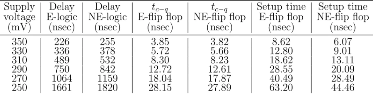
4.1 Comparison between the characteristics of the equalized flip flop (E-flip flop) with the conventional non-equalized master-slave flip flop (NE-flip flop) at different supply voltages operating in sub-threshold regime. Feedback equalization technique reduces the propagation delay of the 8-bit carry-lookahead adder CMOS logic whereas the setup time and
tc−q delay of the conventional flip flop is smaller than the equalized flip
flip. . . 60 4.2 Comparison between the minimum energy point and the corresponding
operating frequency of the equalized logic (E-logic) vs. non-equalized (NE-logic) design of various logic blocks. . . 66 4.3 Energy savings in scaled-down equalized logic compared to baseline
non-equalized and equalized logic at the minimum energy supply volt-age at zero word error rate operation for 8-bit carry lookahead adder. 69 5.1 Comparison between the timing characteristics of the original
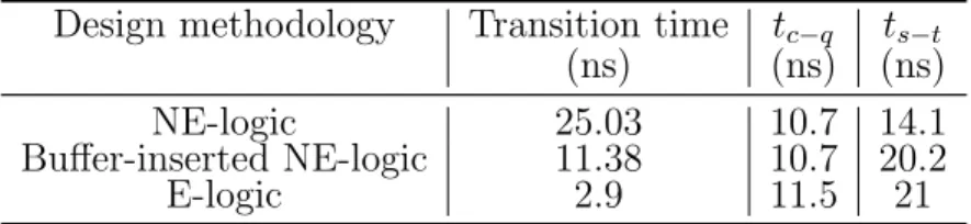
non-equalized design, the non-equalized design with 1 feedback path ON and the buffer-inserted non-equalized design. . . 78 5.2 Comparison between the minimum energy point and the corresponding
operating frequency of the NE-logic vs. E-logic design of various logic blocks. . . 95
and E-logic at the minimum energy supply voltage with zero word error rate operation. . . 95 5.4 Comparison between the total delay, total energy and delay variation
of the digital logic (64-bit adder) at minimum energy supply voltage when the conventional upsizing method (Kwong et al., 2009) has been used together with adaptive feedback equalizer circuit in sub-threshold regime. . . 98 5.5 Comparison between the normalized delay variation and energy-delay
product (EDP) of the equalized logic (E-logic) vs. non-equalized (NE-logic) and buffer-inserted non-equalized design of various logic blocks assuming σVT = 10 mV. . . 99
1·1 Saturation of clock frequency with CMOS scaling process (ISSCC Re-ports 2013). . . 2 1·2 Trend of total power consumption with CMOS scaling process (ISSCC
Reports 2013). . . 3 1·3 Storage capacity of nonvolatile memory technologies (ISSCC Reports
2013). . . 5 2·1 Physical structure of (a)T iO2-based memristor between 2 P tcontacts
consisting of a highly conductive doped region and a highly resistive undoped region, whereL= thickness of the memristor andW = thick-ness of the conductive region, and (b)Hf Ox-based memristor showing
conductive filament growth/narrowing process where φmin and φmax
are the minimum and maximum filament diameters, respectively. . . . 12 2·2 Equivalent resistance of memristor devices. . . 13 2·3 Dynamic window function of the memristor state showing the
nonlin-ear behavior of the memristor for different control parameter p. The current sign function prevents the state from getting stuck at the two boundaries. . . 15 2·4 Rate of diameter change forHf Ox-based memristors in filament growth
model (Ielmini, 2011) for set (V>0) and reset (V<0) operations as a function of voltage across the memristor. . . 16 3·1 1-transistor 1-memristor (1T1R) RRAM cell. . . 22
3·3 Equivalent circuit of 1T1R cell for readsub(left) and writesub/refreshsub
(right) operation. . . 25 3·4 Bitline voltage of a 2-bit/cell T iO2-based RRAM for different bitline
voltage development times. . . 28 3·5 Bitline voltage of a 2-bit/cell Hf Ox-based RRAM for different bitline
voltage development times. . . 28 3·6 Read time of a multi-bit RRAM cell for different number of bits per cell. 29 3·7 Contour plots of the number of consecutive non-destructive read cycles
in multi-bit T iO2-based RRAM for different n andVLL values (x= 0.9). 31
3·8 Contour plots of the number of consecutive non-destructive read cycles in multi-bitHf Ox-based RRAM for different n andVLL values (x= 0.9). 32
3·9 Comparison between analytical model (AM) and HSPICE simulations (HS) for bitline voltage and energy dissipation in differentT iO2-based
andHf Ox-based 2-bit RRAMwrite/ref reshoperation. TheVLL
volt-age is 1.5 V for all transitions. For bitline voltage, the average error is 9.81% forT iO2-based cell and 5.19% for Hf Ox-based cell, while for
energy dissipation the average error is 8.71% for T iO2-based cell and
5.25% forHf Ox-based cell. . . 33
3·10 Contour plots for set time (nsec) in the 2 bits/cell T iO2-based RRAM. 34
3·11 Contour plots for set time (nsec) in the 2 bits/cell Hf Ox-based RRAM. 35
3·12 Contour plots for average read energy (pJ) in multi-bit T iO2 RRAMs.
We maintain at least 25 mV difference between adjacent reference volt-ages for reliable read operation. . . 38
ages for reliable read operation. . . 38 3·14 Energy dissipated in different components of the multi-bitT iO2-based
RRAM array in read operation for uniform (left) and non-uniform (right) state assignments (TR=1nsec). . . 41
3·15 Energy dissipated in different components of the multi-bitHf Ox-based
RRAM array in read operation considering uniform (left) and non-uniform (right) state distributions (TR=200nsec). . . 41
3·16 Energy dissipated in different components of the T iO2-based RRAM
array in write operation (TW=100nsec). . . 43
3·17 Energy dissipated in different components of the Hf Ox-based RRAM
array in write operation (TW=1nsec). . . 43
3·18 Comparison of read time/energy between different memory technologies. 44 3·19 Comparison of write time/energy between different memory technologies. 45 3·20 Uniform state distribution of the multi-bitT iO2-based memristor caused
by OTF. The memristor state distribution for each number of bits/cell is such that maximum process noise margin would be achieved. . . 45 3·21 Non-uniform state distribution of the multi-bitT iO2-based memristor
caused by OTF. The memristor state distribution for each number of bits/cell is such that maximum read noise margin would be achieved. 46 3·22 Uniform state distribution of the multi-bit Hf Ox-based memristor
caused by LER. The memristor state distribution for each number of bits/cell is such that maximum process noise margin would be achieved. 48
caused by LER. The memristor state distribution for each number of bits/cell is such that maximum read noise margin would be achieved. 48 3·24 Diameter change of Hf Ox-based memristors as a function of
tempera-ture for different applied voltages in filament growth model. Diameter shows higher variation with temperature at lower loadline voltages. . 51 3·25 Effective thermal resistance of a 3-bitT iO2-based RRAM as a function
of memristor state. . . 52 4·1 Feedback equalizer (designed using a variable threshold inverter
(Srid-hara et al., 2008)) can be combined with a traditional master-slave flip flop to design an equalized flip flop. . . 59 4·2 DC response of the variable threshold circuit in sub-threshold regime.
The switching threshold of the inverter is modified based on the pre-vious sampled output data. . . 61 4·3 Comparison between the timing waveforms of the input node of the
conventional flip flop (A), output node of the conventional flip flop (B), input node of the equalized flip flop (C), output node of the equalized flip flop (D), output node of the variable threshold inverter (E). Feed-back circuit makes sharper transitions in the waveforms of the logic output node helping the equalized flip flop sample the correct data. . 62 4·4 Operating frequency of the 8-bit carry lookahead adder for zero word
error rate as function of different sub-threshold supply voltages. The equalized logic (E-logic) can run 22.87% (on average) faster than the non-equalized logic (NE-logic). . . 63
ferent supply voltages. At the minimum energy supply voltage, the equalized logic is burning 18.4% less total energy compared to the non-equalized version. . . 64 4·6 Comparison between the energy consumed by the equalized (E-logic)
vs. non-equalized (NE-logic) 8-bit carry lookahead adder for different supply voltages with fixed performance (f = 1.28M Hz) at zero word error rate. The non-equalized logic design consumes minimum energy at 300 mV. The equalized flip flop enables 30 mV supply voltage scaling leading to 16.72% lower total consumed energy. The equalized flip flop cannot operate at VDD < 270mV due to the occurrence of
timing errors. . . 67 4·7 Energy-delay product of the scaled-down equalized 8-bit carry
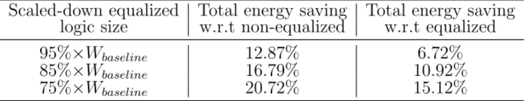
looka-head adder for zero word error rate operation. We can achieve reliable operation even when the transistors in the equalized logic design are scaled down to as small as 75%×Wbaseline. . . 68
4·8 Energy-delay product of a 8-bit carry lookahead adder designed using equalized logic (E-logic) vs. non-equalized logic (NE-logic) at zero word error rate at different technology nodes. The equalized logic approach reduces the energy-delay product of the sub-threshold logic by up to 26.46% across all technology nodes in the minimum energy supply voltage. . . 70
signed using a variable threshold inverter (Sridhara et al., 2008)) can be combined with a traditional master-slave flip flop to design an adaptive equalized flip flop. . . 73 5·2 Circuit diagram of classic master-slave positive edge-triggered flip flop
(Rabaey et al., 2003). . . 74 5·3 DC response of the adaptive feedback equalizer circuit with 2 different
feedback paths in sub-threshold regime. The switching threshold of the inverter is modified based on the previous sampled output data. . 75 5·4 Block diagram of the original non-equalized design (a), equalized design
with 1 feedback path ON (b) and buffer-inserted non-equalized design (c). . . 77 5·5 Comparison between the timing waveforms of the non-equalized logic
design and the equalized logic design of a 64-bit adder. Here, the waveforms include the clock signal (A), input node of the conventional flip flop (B), output node of the conventional flip flop (C), input node of the equalized flip flop (D), output node of the equalized flip flop (E). Feedback circuit enables sharper transitions in the waveforms of the combinational logic output node helping the equalized flip flop sample the correct data. Here the feedback path 2 is OFF. . . 79 5·6 Maximum feedback strength in adaptive equalized flip flop. The
switch-ing threshold of the adaptive equalized flip flop should be larger than the maximum amplitude of the glitch. . . 81
in sub-threshold regime. The average error between the derived model and HSPICE simulation results is 6.96% in the entire sub-threshold regime. . . 82 5·8 Contour plots for the ∆ts−t (ns) of the adaptive equalized flip flop.
Control path strength and feedforward path strength values are nor-malized to minimum-sized transistor sizes. . . 83 5·9 Contour plots for the ∆tc−q (ns) of the adaptive equalized flip flop.
Control path strength and feedforward path strength values are nor-malized to minimum-sized transistor sizes. . . 84 5·10 Contour plots for the tP D−equ (ns) of the critical path in the
equal-ized logic (64-bit adder). Control path strength and feedforward path strength values are normalized to minimum-sized transistor sizes. . . 85 5·11 Comparison between analytical model (AM) contour plots for the total
delay (ns) of the critical path in an equalized 64-bit adder with HSPICE simulations (HS). . . 88 5·12 Comparison between analytical model (AM) contour plots for the
to-tal energy (fJ/operation) of the equalized 64-bit adder with HSPICE simulations (HS). . . 89 5·13 Operating frequency of the 64-bit adder for zero word error rate as
function of different sub-threshold supply voltages. The equalized logic (E-logic) can run 18.91% (on average) faster than the non-equalized logic (NE-logic). . . 91
namic/leakage components of the 64-bit adder for different supply volt-ages. Operating at the respective minimum energy supply voltage, the equalized logic is burning 10.85% less total energy compared to the non-equalized logic. . . 92 5·15 Block diagram of the 32-bit Array Multiplier. . . 93 5·16 Block diagram of the 3-tap 16-bit finite impulse response (FIR) filter. 94 5·17 Energy-delay product of the scaled-down equalized 64-bit adder for
zero word error rate operation. We can achieve reliable operation even when the transistors in the equalized logic design are scaled down to as small as 75%×Wbaseline. . . 96
5·18 Delay distribution of the critical path in the 64-bit adder designed in UMC 130 nm process. The 3 ×σ/µ of the non-equalized logic (NE-logic), the equalized logic (E-logic) with 2 different feedback strengths and the buffer-inserted NE-logic are 16.1%, 11.4%, 7.14% and 15% forσVT = 10 mV at the minimum energy supply voltage, respectively. Here, E-logic designs are operating at 300 mV. . . 97 5·19 Delay distribution of the critical path in the 64-bit adder designed in
UMC 130 nmprocess considering supply voltage variation. . . 100 5·20 Delay distribution of the critical path in the 64-bit adder designed in
UMC 130 nmprocess considering temperature variation. . . 101 5·21 Energy-delay product of a 64-bit adder designed using equalized logic
(E-logic) vs. non-equalized logic (NE-logic) at zero word error rate at different technology nodes. The equalized logic approach reduces the energy-delay product of the sub-threshold logic by up to 23.6% across all technology nodes in the minimum energy supply voltage. . . 102
6·1 Bypass flip flop design . . . 109 6·2 Energy-delay trade-off in combinational logic. Traditional operation
region is around minimum-delay point (MDP). Ultra low-energy region is around minimum-energy point (MEP) (Markovic et al., 2010). . . . 111 6·3 Schematic of the 8T2R Memristor-based Nonvolatile (Rnv8T) SRAM
cell (Chiu et al., 2012). . . 112
Chapter 1
Introduction
1.1
Background and Motivation
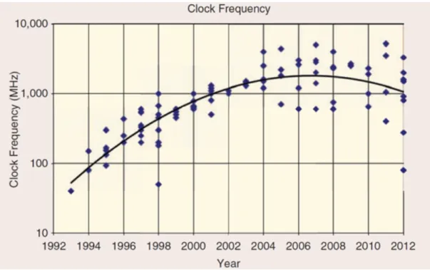
The design of fast and low-power memory and logic circuits is a critical part of design-ing very large scale integration (VLSI) chips that are extensively used today in ap-plications ranging from biomedical implants to handheld devices to laptops/desktops to large data centers. Starting in the 1970’s, the VLSI community was able to use complementary metal-oxide semiconductor (CMOS) technology scaling predicted by Moore’s law (Moore, 1965) to sustain the historic improvement in performance and power of VLSI systems. Nevertheless, as CMOS technology is pushed to its atomic limits, the ability of hardware engineers to achieve power and performance improve-ments with every new technology generation becomes increasingly difficult (Kuhn, 2012; Borkar et al., 2004; Chuang et al., 2007) (Figure 1·1, Figure 1·2). In addition, the performance of most computer systems is increasingly limited by the capacity, ac-cess latency and energy consumption of on-chip memory blocks in today’s computing systems. In particular, the size of the die limits the storage capacity of the memory block. Furthermore, most modern mobile applications require the use of nonvolatile memory to avoid losing data when the power supply is switched off to suppress the dynamic and static power consumption of the digital VLSI chips. Therefore, consider-ing the degradation in CMOS device reliability, the limited available area, the energy
Figure 1·1: Saturation of clock frequency with CMOS scaling process (ISSCC Reports 2013).
and access latency for the design of on-chip memory blocks, it is necessary to explore emerging technologies and alternate circuit-level solutions which are compatible with the conventional CMOS process for designing highly-dense memory arrays. This dis-sertation addresses the use of recently-explored memristor technology to design dense nonvolatile on-chip memory arrays for today’s computer architectures. 1-Transistor 1-memRistor (1T1R) cell based resistive random access memory (RRAM) arrays have low access latency, low access energy and large density (that can allow us to fit the entire working set of an application on the processor chip (Chiu et al., 2012)). Table 1.1 shows a head-to-head comparison of the various nonvolatile emerging tech-nologies. Each technology has its pros and cons, which has made it difficult to identify a successor to CMOS technology. Among these technologies, PCRAM requires large energy for its resistive switching behavior (Chung et al., 2011), FeRAM suffers from signal degradation in scaling process (Qazi et al., 2011) and MRAM has high
en-Figure 1·2: Trend of total power consumption with CMOS scaling process (ISSCC Reports 2013).
durance but it scales poorly and consumes large power due to large write currents (Nebashi et al., 2009). Among these emerging memory technologies, RRAM has been demonstrated to have high density capability due to multi-level cells (MLC) and cross-point array structures (Chen et al., 2009a). RRAM technology (memris-tor) has simple structure, high resistance ratio, fast-switching operation and device scalability beyond 10nmtechnology node (Chiu et al., 2012). Figure 1·3 compares the storage capacity of the emerging RRAM technology with other modern nonvolatile memory technologies. The storage capacity of RRAM technology is approaching the storage capacity of Flash technology. HP Labs has already announced plans to com-mercialize memristor-based RAM and predicted that RRAM could eventually replace traditional memory technologies (Strukov et al., 2008). Therefore, the two-terminal memristor devices have been well-accepted as storage elements and are considered viable replacements to conventional CMOS-based memory designs. The memristor
Memory type PCRAM MRAM FeRAM (Chung et al., 2011) (Nebashi et al., 2009) (Qazi et al., 2011)
Cell 1T1R 1T1R 1T1C
R/W time (ns) 76/20e3 12 200/134
Energy (nJbit) 15.3 0.9/1.3 9.77
Endurance 107 1016 1013
Retention >10 yrs >10 yrs >10 yrs
Density (mmM b2) 15.7 0.35 0.93
Tech. (nm) 58 90 130
Table 1.1: Comparison between current emerging nonvolatile memory technologies.
can be considered as a variable resistor which can be programmed by changing the voltage drop across the memristor or changing the current injected into the memris-tor. Here, programming amounts to changing the value of the memristance which leads to two different states for the memristor. These two states can correspond to storage of logic 0 and logic 1 in the memristor.
The memristor technology can also be used in designing low-energy logic circuits. Although historically higher performance has been the main motivation behind the CMOS scaling process, speed is not the ultimate goal for all modern applications of integrated circuits (ICs). Instead, a wide class of applications are emerging for which power and more importantly energy is the main problem. Ultra-low power sub-threshold circuits are becoming prominent in emerging embedded applications including wireless sensor networks and medical instruments where low energy opera-tion is the main constraint instead of performance.
In sub-threshold circuits, scaling supply voltage into the sub-threshold region signifi-cantly reduces the dynamic energy consumed by digital circuits (Kwong et al., 2009). Scaling the supply voltage also lowers down the leakage current due to reduction in the drain induced barrier lowering (DIBL) effect resulting in considerable lower leak-age power. However, as the supply voltleak-age is scaled below the threshold voltleak-age of
Figure 1·3: Storage capacity of nonvolatile memory technologies (ISSCC Reports 2013).
the transistors, the propagation delay of the logic gates increases enormously leading to the rise in leakage energy of the active devices operating in sub-threshold regime as the leakage power integrates over a longer period of time. As we scale the supply voltage, the two opposite trends in the leakage and the dynamic energy components lead to a minimum energy supply voltage and it has been shown in (Wang and Chan-drakasan, 2005) that the minimum energy supply voltage of digital circuits occurs below the threshold voltage of the transistors.
resulting in a failure in providing rail-to-rail output swings when restricted by aggres-sive timing constraints. Moreover, circuits working in weak inversion region suffer from process variations that directly affect the threshold voltage, which in turn has a significant impact on the drive current due to the exponential relationship between the drive current and the threshold voltage (VT) of the transistors in sub-threshold
regime. These degraded Ion/Iof f ratios and process-related variations thus make
sub-threshold circuits highly susceptible to timing errors which can further lead to complete system failures. Since the standard deviation of VT varies inversely with
the square root of the channel area (Pelgrom et al., 1989), one common approach to overcome the process variation is to upsize the transistors (Kwong et al., 2009). Similarly, increasing the logic path depth to leverage the statistical averaging of the delay across gates has been proposed in (Verma et al., 2008) to overcome process vari-ations. A joint approach of choosing transistor sizes and logic depths that mitigate the impact of process variations has been proposed in (Zhai et al., 2005). Similarly, (Choi et al., 2004) proposes using gates of different drive strengths to overcome pro-cess variations. These approaches, however, increase the transistor parasitics, which in turn increases the energy consumption. Body-biasing approaches have also been proposed to mitigate the impact of variations in (Jayakumar and Khatri, 2005) and (Liu et al., 2011). It however necessitates extra complex on-chip circuitry to generate the required voltage for the substrate terminal of the CMOS devices to reduce the dominant leakage energy of the sub-threshold logic. Therefore, alternate circuit-level approaches are required to alleviate the timing errors while minimizing the energy consumption of the circuit.
1.2
Contribution and Organization
In Chapter 2, we summarize the recent efforts in design and modeling of memristor de-vices and then explain the detailed functionality of our targetT iO2 andHf Ox-based
memristors. We also develop a new state function forHf Ox-based memristor devices
and present it in this chapter. A new reliable SPICE netlist for Hf Ox memristors is
proposed based on the change in the conductive filament diameter.
In Chapter 3, we provide a detailed discussion of the functionality of an n-bit 1T1R RRAM cell followed by a description of the architecture of a memory array designed using this RRAM cell as the building block. We discuss the implementation of mem-ory cells and arrays using both T iO2 and Hf Ox-based memristors. We also discuss
our performance and energy models for the n-bit 1T1R memory arrays designed using
T iO2- andHf Ox-based memristors. We validate our performance and energy models
against HSPICE simulations, and the difference is less than 10% for both n-bitT iO2
-and Hf Ox-based 1T1R cells. Using energy and performance constraints, we
deter-mine the optimum number of bits/cell in the multi-bit RRAM array to be 3. The total write and read energy of the 3 bits/cell T iO2-based RRAM array is 4.06 pJ/bit
and 188 fJ/bit for 100 nsec and 1 nsec write and read access times while the opti-mized 3 bits/cellHf Ox-based RRAM array consume 365 fJ/bit and 173 fJ/bit for 1
nsec and 200 nsec write and read access times, respectively. We explore the trade-off between the read energy consumption and the robustness against process variations for uniform and non-uniform memristor state assignments in the multi-bit RRAM array. Using the proposed models, we analyze the effects of process, voltage and temperature variations on performance and energy consumption and the reliability of n-bit 1T1R memory cells. Our analysis show that multi-bit T iO2 RRAM is more
to Line Edge Roughness (LER) and is more susceptible to voltage and temperature variations.
In Chapter 4, we explore the design of feedback equalizer circuits for digital logic cir-cuits. The key idea here is to explore the use of communications-inspired techniques in the design of robust energy-efficient digital logic circuits. Feedback equalization for above-threshold regime has previously been proposed by (Takhirov et al., 2012) and we explore it for sub-threshold circuits. Using a feedback equalizer circuit that adjusts the switching thresholds of the gates (just before the flip flops) based on the prior sampled outputs, we can reduce the propagation delay of the critical path in the combinational logic block to make the sub-threshold system more robust to tim-ing errors and at the same time reduce the dominant leakage energy of the entire design. We implement a non-equalized and an equalized design of an 8-bit carry lookahead adder in UMC 130 nm process using static complementary CMOS logic. In the equalized design, we could reduce the propagation delay of the critical path of the sub-threshold logic and correspondingly lower the dominant leakage energy, leading to 35.4% decrease in energy-delay product of the conventional non-equalized design at minimum energy supply voltage. Using the feedback equalizer circuit, we obtain 16.72% reduction in energy through voltage scaling while maintaining an oper-ating frequency of 1.28 M Hz. We show that the equalized sub-threshold 8-bit carry lookahead adder requires lower upsizing to tolerate process variation effects leading to 20.72% lower total energy.
In Chapter 5, we propose using an adaptive feedback equalizer circuit in the design of tunable sub-threshold digital logic circuits. This adaptive feedback equalizer circuit can reduce energy consumption and improve performance of the sub-threshold digital logic circuits. At the same time, the tunability of this feedback equalizer circuit enables post-fabrication tuning of the digital logic block to overcome worse than
expected process variations as well as lower energy and improve performance. We implement a non-equalized and an equalized design of a 64-bit adder in UMC 130
nmprocess using static complementary CMOS logic. Using the equalized design, the normalized variation of the total critical path delay can be reduced from 16.1% (non-equalized) to 11.4% ((non-equalized) while reducing the energy-delay product by 25.83% at minimum energy supply voltage. Moreover, we show that in case of worse than expected process variation, the tuning capability of the equalizer circuit can be used post fabrication to reduce the normalized variation (3σ/µ) of the critical path delay with minimal increase in energy. We also present detailed delay and energy models of the equalized digital logic circuit operating in the sub-threshold regime.
Chapter 2
Memristor Technology and Modeling
2.1
Introduction
Memristor is a two-terminal nanodevice that has been recently analyzed for its poten-tial applications in memory design and logic design of both traditional and neuromor-phic computing systems. It is a relatively well-explored device in terms of modeling, design methodology and its physical switching mechanism between two or more sta-ble states. This chapter summarizes the current efforts on design and modeling of memristor devices and then explains the detailed functionality of our targetT iO2 and Hf Ox-based memristors. A new state function that we developed for Hf Ox-based
memristor devices is also presented in this chapter.
2.2
Memristor Device Technology
Memristors provide a functional relationship between the charge and flux which was first postulated in (Chua, 1971). Several oxide-based memristor devices have been proposed as storage elements in the design of RRAM arrays. Hf Ox and T aOx have
been widely used as switching elements in RRAM cells (Chen et al., 2009b), (Chen et al., 2009a), and (Lee et al., 2011). Although several fabricated RRAM prototypes based on different switching materials have been reported in the literature, only a few reliable device models have been proposed for large-scale circuit-level
simula-tions (Ielmini, 2011), (Bersuker et al., 2011), and (Lu et al., 2011). A numerical model of filament growth based on thermally activated ion migration, which accounts for the resistance switching characteristics is proposed in (Ielmini, 2011). This model (primarily developed for Hf Ox-based 1T1R cell) matches the measurement results
for different metal oxide RRAM configurations (Hf Ox/ZrOx, N iO). The authors
in (Guan et al., 2012a) analyze the variation of switching parameters in RRAM de-vices using a trap-assisted-tunneling (TAT) current solver considering the stochastic generation and recombination of oxygen vacancies. The compact model for the pro-posed RRAM switching behavior in (Guan et al., 2012a) is introduced in (Guan et al., 2012b), while the measurement results of the Hf Ox-based prototypes verify
this model in (Yu et al., 2012).
There are multiple efforts in place to develop accurate analytical and SPICE models for the two-terminal memristor elements (Pickett et al., 2009), (Zangeneh and Joshi, 2012), (Ielmini, 2011). An analytical T iO2 memristor model and the corresponding
SPICE code that express both the static transport tunneling gap width and the dy-namic behavior of the memristor state based on the measurement results are proposed in (Pickett et al., 2009) and (Abdalla and Pickett, 2011), respectively. The authors in (Kvatinsky et al., 2013) developed a simplified yet accurate analytical model for the T iO2 tunnel barrier phenomena analyzed in (Pickett et al., 2009) with improved
run times. In (Biolek et al., 2009), the authors developed a mathematical model for the prototype of memristor previously reported in (Strukov et al., 2008) with dependent voltage and current sources as well as an auxiliary capacitor which func-tions as integrator to calculate the state of the memristor. The authors in (Rak and Cserey, 2010) presented a schematic diagram of the memristor SPICE macromodel based on a simplified window function for the rate of change of state. A magnetic flux controlled SPICE model for memristors is proposed in (Batas and Fiedler, 2011)
(a) (b)
L
W
TiO2
TiO2-x
Hf/VO
Figure 2·1: Physical structure of (a)T iO2-based memristor between 2 P tcontacts consisting of a highly conductive doped region and a highly resistive undoped region, whereL= thickness of the memristor andW
= thickness of the conductive region, and (b) Hf Ox-based memristor
showing conductive filament growth/narrowing process whereφmin and
φmax are the minimum and maximum filament diameters, respectively.
based on an exponential relationship for memristor I-V characteristics. In this work we focus on titanium dioxide (T iO2)- and hafnium oxide (Hf Ox)-based memristor
implementations.
The T iO2-based memristor was first fabricated by HP (Strukov et al., 2008). The
fabricated prototype had a highly resistive thin layer of T iO2 and a second
conduc-tive deoxygenizedT iO2−xlayer (see Figure 2·1a). The change in the oxygen vacancies
due to a voltage applied across the memristor modulated the dimension of the con-ductive region in the memristor. This resulted in a high resistance state and a low resistance state corresponding to the resistive and conductive region of operation, respectively. The effective ‘memristance’ of the memristor device can be calculated using Equation (2.1) (proposed in (Strukov et al., 2008)).
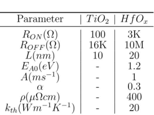
Parameter T iO2 Hf Ox RON(Ω) 100 3K ROF F(Ω) 16K 10M L(nm) 10 20 EA0(eV) - 1.2 A(ms−1) - 1 α - 0.3 ρ(µΩcm) - 400 kth(W m−1K−1) - 20
Table 2.1: Parameters of T iO2-based (Strukov et al., 2008) and Hf Ox-based (Ielmini, 2011), (Sheu et al., 2009) memristors used for
modeling and simulations.
R
OFF
(1-W/L)
R
ON
(W/L)
Figure 2·2: Equivalent resistance of memristor devices.
Here, RON and ROF F are the minimum and maximum memristances, respectively,
andx(t) is the state of the memristor (Eshraghian et al., 2011) (see Figure 2·2). This state of the memristor can be calculated asw(t)/L, wherew(t) is the thickness of the conductive doped region as a function of time, andLis the memristor thickness.
The rate of change of the memristor state follows the ionic drift model which is a function of the memristor physical parameters and the current through the memristor. As the current itself varies with time, the change of memristor state exhibits nonlinear behavior. This nonlinear behavior can be expressed using a window function shown in Equation (2.2) (Eshraghian et al., 2011).
dx dt =
µvRON
L2 i(t)F(x(t), p) (2.2)
In Equation (2.2), µv ≈ 3× 10⁻⁸m2/s/V (Witrisal, 2009) is the average dopant
mobility,F(x(t), p) is the window function, where the parameterpcontrols the mem-ristor nonlinearity. Increasing p yields a flat window function for larger memristor states. Window functions that consider the linear ionic drift, and the nonlinear be-havior that appears at the boundaries of the memristor state, have been proposed in (Benderli and Wey, 2009) and (Joglekar and Wolf, 2009). However, both these window functions get stuck at the memristor state boundaries. We use the window function proposed in (Biolek et al., 2009) for developing the performance and energy models of the T iO2-based RRAM cell. This function models the nonlinear behavior
of the rate of change of state without getting stuck at the boundaries and is given in Equation (2.3).
F(x(t), p) = 1−(x−sgn(−i(t))2p (2.3)
Here, i(t) is the current through the memristor, sgn is a sign function that prevents the state of the cell from getting stuck at the borders andpis the control parameter. Figure 2·3 shows a plot of the window function for different p values.
In case of theHf Ox-based memristor, the set/reset (changing memristor resistance to
RON/ROF F) process is performed by increasing/decreasing the diameter of the
con-ductive filament (CF) using positively charged oxygen vacancies (VO) orHf ions
mi-gration in a thermally activated hopping process in the filament growth model (Ielmini, 2011). Applying a voltage across theHf Ox-based memristor forces the positive ions
tem-0
0.2
0.4
0.6
0.8
1
0
0.5
1
Memristor State (x)
Window Function F(x,p)
p=2
p=4
p=6
p=8
Figure 2·3: Dynamic window function of the memristor state showing the nonlinear behavior of the memristor for different control parameter
p. The current sign function prevents the state from getting stuck at the two boundaries.
perature along the CF and changing the effective cross section diameter of the CF (see Figure 2·1b). This rate of change of diameter was derived in (Ielmini, 2011) and is given by
dφ dt =Ae
− EA0−αqV
kT0(1+8T0Vρkth2 ) (2.4)
where,φis the CF diameter, A is a pre-exponential constant,EA0is the energy barrier
for ion hopping, α is the barrier lowering coefficient,q is the elementary charge, V is the applied voltage across the memristor,k is the the Boltzmann constant, T0 is the
room temperature,ρis the electrical resistivity andkthis the thermal conductivity. A
similar expression with a negative rate of change is used for modeling the reset process inHf Ox-based memristors. As voltage is applied across theHf Ox-based memristor,
−4 −2 0 2 4 6 8 −0.5 0 0.5 1 V (V) d φ /dt (m/s)
Figure 2·4: Rate of diameter change for Hf Ox-based memristors in
filament growth model (Ielmini, 2011) for set (V>0) and reset (V<0) operations as a function of voltage across the memristor.
according to R(t) = 4ρL/πφ(t)2. The rate of change of the diameter for Hf O
x
-based memristors in filament growth model for set and reset operations is shown in Figure 2·4. The nominal parameter values of the memristor used for generating this plot are listed in Table 2.1. To minimize the destruction of the stored data during read operation, we maintain the voltage across the memristor to be greater than -1.7
V. Similarly, during write operation we maintain the applied voltage between 1 V to 4 V to minimize the set operation time.
To find the instantaneous memristance of the Hf Ox RRAM, we define a new state
function for Hf Ox memristors as in Equation (2.5).
x(t) = C 1− φ 2 min φ(t)2 ! (2.5)
where the coefficient C is
C = φ 2 max φ2 max−φ2min = (1−1/β) (2.6)
Here, φmax and φmin are the maximum and minimum CF diameters corresponding
to RON and ROF F, and β = ROF F/RON. This state function can be plugged into
equation (2.1) to calculate the effective memristance. Considering the rate of change of the CF diameter in (2.4) and the state function in (2.5), we define the rate of change of the Hf Ox-based memristor state in Equation (2.7).
dx dt = 2Cp(1−x/C)3 φmin dφ dt. (2.7)
The corresponding HSPICE netlist that we developed forHf Ox-based memristors is:
.SUBCKT memristorHfOx PLUS MINUS phi .PARAM phimin=’sqrt(4*ro*L/(3.14*Roff))’ .PARAM phimax=’sqrt(4*ro*L/(3.14*Ron))’ .PARAM C=’phimax*phimax/(phimax*phimax-phimin*phimin)’ Csv phi 0 1 .IC V(phi) 0.3
Emem PLUS AUX VOL=’I(Emem)*(V(phi)*Ron+ (1-V(phi))*Roff)’
Rtest AUX MINUS 1 Gsv 0 phi
CUR=’C*phimin*phimin*POW(sqrt(phimin*phimin /(1-(phimax*phimax-phimin*phimin)*V(phi)/ (phimax*phimax))),-3)*2*A*exp(-1*(EA0-alpha*
q*V(PLUS,MINUS))/(k*T0*(1+POW(V(PLUS,MINUS)
,2)/(8*T0*ro*kth)))) * sgn(I(Emem)) * sgn((1-V(phi)+ sgn(sgn(-I(Emem))+1))) * sgn((sgn(V(phi))+
sgn(I(Emem))+1))’ .ENDS memristorHfOx
The rate of change of the Hf Ox-based memristor state is modeled as a
voltage-controlled current source, and the combination of sgn functions guarantees the re-liable set/reset operations, and the normalized memristor state does not get stuck when approaching 1 or 0.
2.3
Summary
In this chapter, we first described the behavioral functionality of theT iO2 memristor
based on the ionic drift model. We then proposed the state function for the Hf Ox
-based memristors. A new reliable SPICE netlist forHf Ox memristors was proposed
Chapter 3
Design of Multi-bit RRAM Array
3.1
Introduction
In Chapter 2 we provided a detailed description of the memristor technology. In this chapter we provide a detailed discussion of the functionality of an n-bit 1T1R RRAM cell followed by a description of the architecture of a memory array designed using this RRAM cell as the building block. We discuss the implementation of memory cells and arrays using both T iO2 and Hf Ox-based memristors. We also discuss our
performance and energy models for the n-bit 1T1R memory arrays designed using
T iO2- and Hf Ox-based memristors.
3.2
Related Work
Several memory circuit/architecture topologies have been proposed in the literature based on the memristive structures. The authors in (Jo et al., 2009) used a Si-based memristive system to fabricate high-density crossbar arrays with high yield and OFF/ON ratio. A memristor-based T iO2 memory cell is introduced in (Ho
et al., 2011) and its functionality is evaluated using system-level simulations. An energy-efficient dual-elementT iO2-based memory structure is proposed in (Niu et al.,
2010a), in which each memory cell contains two memristors that store the comple-mentary states. Similarly, a 2-bit storage memristive cell is proposed in (Manem and
Rose, 2011). Both these multi-bit memory cells have large area. Content addressable memory (CAM) designed usingT iO2 memristors has been introduced in (Eshraghian
et al., 2011). A memristor-based Look Up Table (LUT) design has been introduced in (Chen et al., 2012) to replace the SRAM-based FPGA design while achieving higher density. In (Fei et al., 2012), the functionality, performance and power of several CMOS/memristor based circuits with memory applications have been verified using a simulator based on a Modified Nodal Analysis. An analysis of the periph-eral circuitry of the crossbar array architecture is presented in (Xu et al., 2011). A nonvolatile 8T2R SRAM cell that uses two Hf Ox-based 1T1R cells along with the
conventional 6T SRAM structure is introduced in (Chiu et al., 2012) for low power mobile applications. A bridge-like neural synaptic circuit with 5T iO2-based
memris-tors which is capable of performing sign/weight setting and synaptic multiplication operations is introduced in (Kim et al., 2012b). A memristor emulator composed of the basic circuit-level elements is designed in (Kim et al., 2012a). The authors in (Liauw et al., 2012) presented a 3D-FPGA with stacked RRAM technology achieving lower energy-delay product (EDP) and smaller area compared to the conventional 2D-FPGA design. In (Xue et al., 2012), the authors proposed adaptive write and read circuits for RRAM arrays to enhance yield and β ratio while eliminating large power consumption rising from the resistance fluctuations.
Memristors are highly vulnerable to process variation and several authors have ana-lyzed its impact on the functionality of the memristive structures. Line-Edge Rough-ness (LERs) caused by uncertainties in the process of lithography and etching (Jiang et al., 2009), Oxide Thickness Fluctuations (OTFs) caused during sputtering or atomic layer deposition, and Random Discrete Doping (RDDs), which leads to ran-domness in resistivity of the conductive as well as the resistive region of the memristor, are generally the main causes of process variations. The authors in (Niu et al., 2010b)
have analyzed the effect of cross section area and oxide thickness variations on the memristor resistance. The authors in (Hu et al., 2011a) have analyzed the effect of LER and OTF on the statex(t), the rate of change of statedx(t)/dt and power dissi-pation variations of T iO2-based memristor. Using an Error Correcting Code (ECC)
design that is commonly used in conventional DRAM memory, the authors in (Niu et al., 2012) propose the detection and mitigation of errors rising from process vari-ations in both MOS-based and crossbar memristive RRAM cells. The authors in (Sheu et al., 2011) have used a Parallel-Series Reference-Cell (PSRC) scheme to de-crease the reference current fluctuations in 1T1R RRAM structure. Moreover, using a Process-Temperature-Aware Dynamic BL-bias (PTADB) circuit, they lower the read disturbance caused by bitline voltage variations.
We present the detailed energy and performance models of multi-level 1T1R RRAM cells that use T iO2- andHf Ox-based memristors. For theHf Ox-based array design,
we use the filament growth model in (Ielmini, 2011) that has been validated against measurement results. We determine the optimum number of bits per RRAM cell that consumes the least energy while being constrained by cell performance. We apply the Monte-Carlo methodology in (Hu et al., 2011a) to model the effects of LER, OTF and RDD on the functionality of multi-bitHf Ox as well asT iO2 RRAM cells.
3.3
RRAM Cell Design
The circuit of the 1T1R RRAM cell is similar to a DRAM cell and consists of an access transistor and a memristor as storage element (see Figure 3·1). Similar to DRAM, the access transistor is enabled for both read and write operations. As the memristor device shows considerable nonlinearity when approaching the states of 0 (Rm =ROF F) and 1 (Rm =RON), it increases the required set/reset operation times
LL
BL
WL
M
em
rist
or
X
Figure 3·1: 1-transistor 1-memristor (1T1R) RRAM cell.
at the two boundaries. We therefore ignore the states smaller than 0.1 and larger than 0.9 for faster set/reset i.e. write operations. The n bits of a cell are stored in the 2n distinct sub-ranges in the range of 0.1 to 0.9. For an n-bit cell design, the
state assignment can be done such that maximum noise margin would be achieved. For example, for a 2-bit RRAM cell, a memristor state below 0.3 corresponds to 00, a memristor state between 0.3 and 0.5 corresponds to 01, a memristor state between 0.5 and 0.7 corresponds to 11 and a memristor state above 0.7 corresponds to 10. We use Gray coding to increase the robustness and minimize the probability of getting two bits in error in the read operation. We refer to this assignment as uniform state assignment. A non-uniform state assignment could also be used for the n-bit cell. A comparison of the two assignments is presented in Section 3.8.
To perform the read operation, the loadline is driven to charge the bitline through the memristor and access transistor. The read operation of the n-bit RRAM cell may be destructive and could require periodic refreshing of the cell data. For threshold-based memristor technologies recent measurement results have shown that if the drive voltage is less than a threshold, the state does not change for fast read operations (see Figure 2·4). The T iO2 RRAM - based on the ionic drift model - is not a
threshold-based technology (Kvatinsky et al., 2013) and shows more destructiveness during read cycles. A detailed analysis of the read destructiveness in multi-bit RRAM cells is proposed in Section 3.5.
The write operation always consists of two sub-operations – read followed by write as we need to know the data currently stored in the cell to determine the exact voltage that needs to be applied across the memristor to write new data. To perform the write operation, a positive or negative voltage is applied across the memristor for transitions to higher or lower states, respectively. The current flowing through the memristor changes the size of conductive region (in ionic drift model) or changes the diameter of the conductive filament (in filament growth model), thus increasing or decreasing the ‘memristance’. In the rest of the thesis, we refer to the memory read and write operations as readtop and writetop, and the sub-operations as readsub,
refreshsub and writesub. Thus readtop = readsub + refreshsub, while writetop = readsub
+ writesub.
3.4
RRAM Array Architecture
The overall architecture of a memory array built using 1T1R RRAM cells is similar to the conventional DRAM array i.e. a wordline is used to select a row of cells, and a bitline is shared by the cells in a column for reading/writing (see Figure 3·2). In
Wordline B itli ne ADC circuit Wordline driver 2n -bi t DA C P re-disch a-rge ci rcui t 2:1 B in 0 B in 1 B in 2 B in 2n -1 V BL V ref 2 n -1 SA SA SA V ref 2 V ref 1 Bout 0Bout1 Boutn-1 Loadline Loadline driver Thermometer-to-Binary decoder 1T 1R n -bi t cel l WL BL LLM em rist or X
Figure 3·2: n-bit/cell RRAM array architecture.
an RRAM array architecture, to perform the readsub operation, we first discharge
the bitline (BL) to 0 V, and then enable the wordline (WL) and loadline (LL) for a fixed predefined time. For the n-bit/cell array, when the WL and LL are enabled, the bitline charges to one of the 2n distinct voltages corresponding to the 2n distinct
data values (i.e. the memristor state) stored in the cell. For instance in a 2-bit/cell array, there will be 4 distinct data values. An analog-to-digital converter (ADC) can be used to retrieve the n bits in each cell during the read operation. Each n-bit ADC consists of 2n−1 differential sense-amplifiers, each having the V
BL as one input and
a unique reference voltage (Vref i) as the other input. For example a 2-bit/cell array
needs 3 differential sense amplifiers. The 2n−1 sense amplifiers are shared by all
the cells in the column. The sense amplifiers could be shared between columns to relax the area constraints on sense amplifier design. The rail-to-rail outputs of the sense amplifiers are fed to thermometer-to-binary code decoders that determine the exact data stored in the n-bit 1T1R cell and is given by bit Bout
0 to Boutn−1. We use
Cd DAC Rtg Rch Rm VLL CBL/n RBL/n CBL/n RBL/n CBL/n RBL/n Cd Rch Rm VLL CBL/n RBL/n CBL/n RBL/n CBL/n RBL/n
Figure 3·3: Equivalent circuit of 1T1R cell for readsub (left) and
writesub/refreshsub (right) operation.
a short critical path and consumes low power.
To perform the writesub operation, one of the 22n−2n different voltages
(correspond-ing to the 2n(2n−1) possible transitions for the n-bit RRAM cell) need to be applied
across the memristor. For example, a 2-bit/cell array needs 12 voltages corresponding to 12 different transitions. The refreshsub operation would be similar to the writesub
operation and the applied voltage will depend on the mechanism used for refresh op-eration. A 2n-bit multiplexer-based digital-to-analog converter (DAC) can be used to generate the voltages to be applied across the memristor for writesub/refreshsub
operation. During writesub/refreshsub operation, the outputs Bout0 and Boutn−1 are
con-nected to the Bin
0 and Binn−1 inputs (corresponding to the current stored bits) and the
data to be written into the cell is connected to the Binn and Bin2n−1 inputs of the 2n-bit DAC. This ensures the DAC generates the correct voltage to be applied to the bitline for writing the data. For the 2-bit/cell array, we need a 4-bit DAC that generates 12 different set/reset voltages and an ADC with 3 sense amplifiers.
3.5
Performance Models
As discussed in Section 3.3, the readtop and writetop operation of the n-bit 1T1R cell
consists of readsub + refreshsub and readsub + writesub operations, respectively. The
equivalent circuit model for the 1T1R RRAM cell during readsub operation is shown
in Figure 3·3. Here,Rm is the equivalent time-variant resistance of the memristor and
transmission gate which is part of the pre-discharging path of the bitline capacitor is not included here as that transmission gate is switched OFF as soon as BL is discharged resulting in very high equivalent resistance for the transmission gate. CBL
andCdare the bitline capacitor and access transistor junction capacitor, respectively.
AlsoRBLis the total resistance of the bitline. The bitline voltage at the end of readsub
operation (i.e. after time TR) will be
VBL =VLL(1−e
−TR
(Rm(t)+Rch+0.5RBL)CBL). (3.1)
Here the time constant of the junction capacitor (Cd) is much smaller than that of the
bitline capacitor (CBL), and hence CBL +Cd has been approximated to be equal to
CBL. Also, the term 0.5RBLCBLis the intrinsic time constant of the bitline modeled as
a distributedRC-line. We assume the bitline, wordline and loadline to be 1mmlong, each with total capacitance of 200 f F and total resistance of 6.5 KΩ corresponding to copper metal line with 50nm ×50nmcross-section area. In addition, we assume the distributed RC-line model with 80 segments for all of the interconnects in the RRAM array architecture. For a n-bit RRAM cell, equation (3.1) can be used to define the 2n−1 reference voltages to be input to the sense amplifiers that are used to
differentiate between the different stored values while performing readsub operation.
For example, for a 2-bit RRAM cell, we can use equation (3.1) to determine the three different reference voltages to differentiate between the four different stored values. The bitline voltage depends on the data stored in the memristor, i.e. the memristor state. For Vref1 > VBL, Vref1 < VBL < Vref2, Vref2 < VBL < Vref3
and Vref3 < VBL the stored data is 00, 01, 11 and 10, respectively. In Table 3.1
and Table 3.2, we compare the reference voltages calculated using the analytical model shown in Equation (3.1) and using HSPICE simulation using 22 nm PTM technology (Ptm, ). The parameters of T iO2 and Hf Ox-based memristors that are
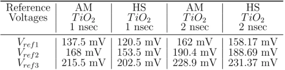
Reference AM HS AM HS
Voltages T iO2 T iO2 T iO2 T iO2
1 nsec 1 nsec 2 nsec 2 nsec
Vref1 137.5 mV 120.5 mV 162 mV 158.17 mV
Vref2 168 mV 153.5 mV 190.4 mV 188.69 mV
Vref3 215.5 mV 202.5 mV 228.9 mV 231.37 mV
Table 3.1: Comparison between the reference voltages determined using analytical model (AM) and HSPICE simulation (HS) for a readsub
access time of TR(T iO2) = 1, 2 nsec in the 2-bit/cell 1T1R RRAM. VLL(T iO2) = 0.48 V is chosen to reach to at least 25 mV difference
between the two adjacent reference voltages. The average error is 5.7% for T iO2.
Reference AM HS AM HS
Voltages Hf Ox Hf Ox Hf Ox Hf Ox
200 nsec 200 nsec 400 nsec 400 nsec
Vref1 94.5 mV 94.79 mV 100.85 mV 100.84 mV
Vref2 130.5 mV 130.9 mV 135.25 mV 135.23 mV
Vref3 214 mV 214.6 mV 204.8 mV 204.81 mV
Table 3.2: Comparison between the reference voltages determined us-ing analytical model (AM) and HSPICE simulation (HS) for a readsub
access time of TR(Hf Ox) = 200, 400 nsec in the 2-bit/cell 1T1R
RRAM. VLL(Hf Ox) = 0.7 V is chosen to reach to at least 25 mV
difference between the two adjacent reference voltages. The average error is 0.151% for Hf Ox.
used in modeling and HSPICE simulations are summarized in Table 2.1. Here the read time of 1, 2 ns (for T iO2) and 200, 400 ns (for Hf Ox) is chosen based on the
nominal β value for the two types of memristors (see Table 2.1). Hf Ox has larger
β and ROF F values compared to T iO2, and therefore it needs higher read time for
reliable read operation. If we ignore the destructiveness (changing the memristance) during readsub in the analytical model for simplicity, the resulting average error is
5.7% for T iO2 and 0.151% forHf Ox.
To ensure a reliable read operation, there should be sufficient difference in the four different voltages developed on the bitline corresponding to the 4 different data that can be stored in the 2-bit cell. For very large bitline voltage development times, the
0 2 4 6 8 10 0 0.1 0.2 0.3 0.4 0.5
Bitline voltage development time (nsec) V BL
(V)
Figure 3·4: Bitline voltage of a 2-bit/cellT iO2-based RRAM for
dif-ferent bitline voltage development times.
0 0.5 1 1.5 2 2.5 3 0 0.2 0.4 0.6 0.8
Bitline voltage development time (µsec) V BL
(V)
Figure 3·5: Bitline voltage of a 2-bit/cell Hf Ox-based RRAM for
different bitline voltage development times.
bitline can get completely charged to the load line voltage (VLL). At the same time,
for very small bitline voltage development times, the difference in the bitline voltages may not be large enough for the sense-amplifiers to correctly determine the data stored in the cell. The bitline voltage of T iO2- and Hf Ox-based 2-bit/cell RRAM
Figures 3·4 and 3·5, respectively. For our 2-bit/cell RRAM array example, we design our sense amplifier such that it needs at least 12.5 mV differential inputs. Hence, we need at least 25 mV difference between the adjacent bitline voltages corresponding to the 4 different data that can be stored in the 2-bit cell. The Vref inputs to the
three sense amplifiers are chosen based on bitline voltages (corresponding to the four different data that can be stored in the cell) while ensuring the 12.5 mV differential input. So for the T iO2- and Hf Ox-based 2-bit/cell RRAM cells we choose bitline
development time of 1 nsec and 200 nsec, respectively. In the T iO2-based cell, for
the 1 nsec read access time, the four different bitline voltages are 125 mV, 150 mV, 186 mV and 245 mV. The corresponding Vref1, Vref2 and Vref3 values are 137.5 mV,
168 mV, and 215.5 mV, respectively. Similarly, in the Hf Ox-based cell, for the 200
nsec read access time, the four different bitline voltages are 82 mV, 107 mV, 154 mV and 274 mV. The corresponding Vref1, Vref2 andVref3 values are 94.5 mV, 130.5 mV,
and 214 mV, respectively. The read times as a function of number of bits/cell (n) is illustrated in Figure 3·6. These read times have been chosen using the same approach as described above for the 2 bits/cell RRAM cell. As the value of n increases, we need larger read times to ensure the reliable read operation.
As discussed in section 3.3, the readsub operation of the 1T1R cell can be destructive.
The read destructiveness of T iO2-based memristors is larger compared to Hf Ox
-based memristors for the same loadline voltage (VLL). The T iO2-based memristor
therefore needs to be refreshed more frequently than Hf Ox-based memristor.
Con-sidering the rate of change of state for T iO2 RRAM in Equation (2.2), the number of
consecutive read operations that will not destruct the stored data in multi-bit T iO2
-based 1T1R RRAM cell, i.e. the refresh threshold can be written as (Zangeneh and Joshi, 2014a)
1 2 3 4 10−9 10−8 10−7 10−6 10−5
Number of bits per cell
Read Time (sec)
TiO 2 HfO
x
Figure 3·6: Read time of a multi-bit RRAM cell for different number of bits per cell.
tref−T iO2 ≈
(xmax−xmin)(Rm(x) +Rch)
2nγT
RVLL(1−(x−1)2p)
. (3.2)
Here, Rm(x) is the resistance of the memristor for each state, n is the number of
bits/cell, TR is the read access time, xmax and xmin are the maximum and minimum
normalized memristor states (0.9 and 0.1 in this work), respectively and γ = µvRON
L2 . Large VLL, n and RON values (smaller β) necessitate more frequent refresh
opera-tion in the multi-bit RRAM cell. The contour plots of the number of consecutive non-destructive read operations in multi-bit T iO2 RRAM is shown in Figure 3·7 for
different n (number of bits/cell) and VLL values for a memristor with initial state of
x = 0.9. In case of the highly destructive multi-bit T iO2 memristor, we explored
two different refresh schemes: A refresh operation can be performed after each read cycle to compensate for destructiveness (Niu et al., 2010b). In this refresh scheme, we apply a -VLL for the same duration as readsub. This doubles the read energy and
2 2 5 5 5 10 10 10 10 20 20 20 20 50 50 50 80 80 80 100 100 100 200 200 300 300 V LL (V) n 0.1 0.2 0.3 0.4 0.5 0.6 0.7 0.8 0.9 1 1 2 3 4 5
Figure 3·7: Contour plots of the number of consecutive non-destructive read cycles in multi-bit T iO2-based RRAM for different
n and VLL values (x= 0.9).
counter to track the current state of the memristor as well as the number of consecu-tive read operations. A refresh operation is done once the number of consecuconsecu-tive read operations on the multi-bit T iO2 RRAM cell exceeds the threshold. For instance,
in a 3-bit/cell T iO2-based RRAM array with VLL = 0.1 V, 50 consecutive read
cy-cles will result in loss of data (see Figure 3·7), so a 6-bit counter will be required to track the magnitude of destructiveness and perform refresh operation. Although the counter-based refresh approach seems more beneficial in multi-bit T iO2 RRAM
compared to the read followed by refresh scheme, our analysis shows that the energy and area overhead of the counter-based approach makes it infeasible.
Considering the rate of change of state for Hf Ox RRAM in Equation (2.7), the
number of consecutive non-destructive read operations in multi-bitHf Ox-based 1T1R
RRAM cell will be
tref−Hf Ox =
φmin(xmax−xmin)
2n+1T RC p (1−x/C)3dφ dt . (3.3)
100 100 1e 4 1e 4 1e 6 1e 6 1e 8 1e 8 1e10 1e10 1e12 1e12 1e14 1e16 1e18 V LL (V) n 0.1 0.2 0.3 0.4 0.5 0.6 0.7 0.8 0.9 1 1 2 3 4 5
Figure 3·8: Contour plots of the number of consecutive non-destructive read cycles in multi-bit Hf Ox-based RRAM for different
n and VLL values (x= 0.9).
The corresponding contour plots of the number of consecutive non-destructive read operations for different n and VLL values for a memristor with initial state of x= 0.9
is shown in Figure 3·8. The threshold-based conductive filament growth mechanism inHf Ox memristor makes it more resilient to read destructiveness compared to
ion-drift mechanism based T iO2 memristors. As can be seen in Figure 3·8, for small
read voltage values a large number of consecutive read operations are required to de-struct the current state in multi-bitHf Ox RRAM technology. The refresh threshold
proposed in Equation (3.3) and shown in Figure 3·8 exceeds the maximum allowed number of accesses (endurance) in the Hf Ox-based RRAMs reported in (Sheu et al.,
2009) (see Table 1.1) and (Chiu et al., 2012) which practically makes Hf Ox a
non-destructive memristor technology at small read voltages. In case large voltages are used forreadsub operation, then we might observe destructiveness of memristor state.
To combat this, we propose to use a counter that tracks the current state of the memristor as well as the number of consecutive read operations. A refresh operation is done once the number of read operations exceeds the threshold given by Equation