•
•
•
•
•
PRECISION
:~
TYPE
•
'-"" RT
jf
30E:
•
DISPLAY
j
•
•
•
PRECISION
CRT
•
•
•
•
•
•
•
•
•
•
•
•
•
•
•
•
•
•
DISPLAY
•
•
•
•
•
•
TYPE
COpy NO.
1
OJ 2
This manual contains proprietary information. It is provided to the cus-tomers of Digital Equipment Corporation to help them properly use and maintain DEC equipment. Revealing the contents to any person or organization for any other purpose is prohibited.
Section
2
3
4
5
TABLE OF CONTENTS
D.-~r~_~
rlc.YL.t:: • • • • • • • • • • • • • • • • • • • • • • • • • • • • • • • • " v
General Description... 1-1
Interface 5i gna Is .••...••••••••..•••..•.• 2-1
Si9nal Description •..••••••.•••••. 2-1
Input Signais .•.•••.•.•••••••••••• 2-1
Output Signals .•••••••••••.•••••. 2-1
Logical Operation ..••••••••••••.• , .•••••
Coordinate Channels .. " ... ,,""""""""
Deflection Circuits .••••••••••••••
Control and Timing Circuit ••••••••.
Status and intensity Circuit .••.•••.•
Intensity Bias Circuit .•••.•.•••••••
I nd i ca tors C i rcu it ••••••.••••••.••.
Electrical Power .•••.••••••••••.•.
Maintenance ...••••••.••••.•••.•••••••••
3-1
3-2
3-6
3-9
1"\ l '
,,:)-11
3-13
3-14
3-15
4-1
Special Tools and Test Equipment.... 4-1
Assembly and Disassembly •••••••••• 4-1
Ad i ustmen ts ..••••....••••••••.••. 4-2
Periodic Maintenance ••••••••••••• 4-8
Troubleshooting. . . •• ••. •• • •• • • • •• .
4-9
Diagrams •...•..••.•••••.•.••..••.••.•••
5-1
Cable Schedu Ie ••••..•...•...•.•
5-2
LIST OF TABLES
Table Page
1-1 Physical Specifications 0 0 0 0 0 0 0 0 0 0 0 0 0 0 0 0 • • 0 0 0 0 0 0 . 0 • • 0 0 1-1
1-2 Operating Specifications 0 0 0 0 0 0 . 0 • • 0 0 . . . 1-4
3-1 Coordinate Channel Logic Conversion Table .•••••••• 0 • • • 3-5
3-2 Intensity Correlations •••••• 0 0 • • • 0 0 0 . 0 • • • • o . • • • . . . • • • • 3-12
4-1 Special Tools and Test Equipm~,nt . 0 0 0 0 • • • • • • • • 0 • • • 0 0 . 0 4-1
4-2 10-Bit Digital-to-Analog Converter Adjustment ••••• 0 0 0 . 4-3
4-3 Possible CRT Beam Malfunctions ••••• 0 0 0 • • • 0 . . . 0 • 0 • • • • 0 4-9
4-4
Specific Malfunctions 0 • • • 0 • • • • • • 0 • • • • • 0 • • 0 • • • • • • • 0 • • 4-105-1 List of Diagrams 0 • • • 0 • 0 .. 0 0 • 0 • • 0 0 0 0 0 • • • 0 0 • 0 0 • 0 0 • • 0 0 0 0 5-1
Figure
1-1
1-2
3-1
3-2
3-3
3-4
3-5
3-6
3-7
4-1
4-2
LIST OF ILLUSTRATIONS
Type 30 Precision CRT Display •• 0 . 0 0 0 . 0 . 0 0 0 . 0 0 0 • • 0 0 0 0
Type 30E Logic Panel and Power Supply Locations. 0 0 . 0 • •
Type 30E Block Diagram o . 0 0 0 o . 0 0 0 . 0 0 0 • 0 0 0 0 • 0 0 0 0 0 • o • •
Type 30E Coordinate Channels Logic Block Diagrams. 0 • • 0
Deflection Circuit Block Diagram 0 0 • • 0 0 0 • • • • • • • • 0 • 0 0 0 •
Deflection Compensation Characteristics ••••• 0 • • 0 0 0 0 0 0 0
Control and Timing Circuit Logic Block Diagram •••• 0 0 0 0
Status and Intensity Circuit Logic Block Diagram .•• 0 0 0 0 0
Intensity Bias Circuit Logic Block Diagram o. 0 0 0 • • 0 0 0 0 0 0
Type 1564 Ad justment Locations .. 0 0 • 0 0 0 0 0 • • 0 • 0 • 0 • 0 0 0 0
Type 1567 Adjustment Locations
...
vi1-4
3-1
3-3
3-7
3-8
3-10
3-11
3-13
4-4
PREFACE
This manual is intended for use with the Type 30A, Type 30E, and
Type 30M Precision CRT Displays. These three types of displays are
identical in operation and circuitry, and only differ in slight degree
with respect to their use. The Type 30A does not contain the five
BNC connectors which allow an external oscilloscope to be used for
monitoring purposes. The Type 30M contains a reversing switch that
allows the horizontal and vertical axes of the display to be
inter-changed.
Engineering drawings and schematics may become outdated over a
period of time. If the equipment does not resemble the printed
drawing or schematic, request a print for your particular equipment
SECTION 1
GENERAL DESCRIPTION
The Type 30E Precision CRT Displcy shown in Figure 1-1 is an ancillary equipment designed
to be used with digital computers. It is a random-position, point-plotting cathode ray tube
with a control unit and power supplies mounted in a table = The equipment receives X and Y
coordinate information in two ten-·bit words and, on command, displays a spot of light on the
screen of a cathode ray tube at this translated position. Discrete points may be plotted in any
sequence at a 20 kilocycle rate {one point every 50 microseconds}. Provision is made for a
Light Pen to be used for identification and selection of any specific display area, and for an
external monitoring oscillos:-:ope to repeat the display.
The Type 30E Precision CRT Display consists of a 16-inch cathode ray tube in an adjustable
mounting and a table with a!1 the electronic equipment mounted beneath it: Figure
1-2
showsthe outl ine of the equipment and the location of various panels.
Dimensions
Coior
Weight
Mounting
Clearance
Display Tube
I
r . . L • . '-l
Lonrrol>TABLE 1-1 PHYSICAL SPECIFICATIONS
50 inches wide, 34 inches deep, 24 inch table height, 49 inches overall height.
Biue and Gray Tweed uniess specified.
360 pounds.
All circuits and power sJPplies are mounted on or under a table. The table legs have adjustable feet for leveling, and normally support 75-100 pounds each whp.n properly adjusted.
Access room for main"terence requires 3 feet in the rear and 2 feet above.
The CRT housing can be tilted approximately 5° forward, 20° back-ward, an.] 60° sideways. Full 360° rotation is possible by removing
the stop bolts. A 1/811
thick sheet of form-fitted plexiglass protects the face of the CRT.
TL _ _ ~_ I _ ~ _____ ~ >-0 ~_ _ _ ~_ ' - _ _ I ° __ ~ I ° L L n _ ~_ ,... _ . _ __ L _ I I _ _~ • __ I __ I __ _
Ine OnlY operaTing conrrol I~ U Llgnr ren \.:lain conrrOI locarea unaer
the ri ght front corner of the CRT housing.
REAR VIEW
OPEN
INDICATOR PANEL
OPEN
LIGHT PEN GAIN
TYPE 811 POWER CONTROL
PANEL
OPEN
115 VOLT AC LINE CABLE ~==~!)
TYPE
770
POWER SUPPLY
TYPE
722
POWER SUPPLY
EQR POWER SUPPLY
INPUT CABLE j--~
DEFLECTION AMPLIFIER
BUFFER AND CONTROL LOGIC CIRCUITS
OPEN
FRONT VIEW
Viewed from the front, the CRT housing is mounted on the left-hand side of the table (See
Figure 1-2)" The indicator panei is mounted directly beneath it under the table top. The
right hand mounting area contains a Type 811 Power Control. Both the indicator panel and
the power control panel are covered with easily removable trim panels.
trim panels: On the left, a Type 770 Power Supply which supplies + 10,000 volts, +250 volts,
-150 volts and 6.3 volts ac to the cathode ray tube; a Type 722 Power Supply which supplies
+ 10 volts and -15 volts to the logic circuits; and an NJE regulated 50~volt power supply* for the deflection circuits. The right hand mounting area contains a speciai panel in level
A which holds two pluggable resistor stack assemblies and a heat sink assembly. These
assem-bl ies comprise the output stages of the two deflection ampl ifiers. Directly beneath in level B
is the logic circuit mounting pane!. The third mounting pane! (level C) is left blank.
Be-tween the two lower mounting panels is the deflection reversing switch. The BNC connectors
for use with an external oscilloscope are located inside the center mounting strip with the
input cabie socket.
The logic 'circuit panel and the deflection output amplifier are mounted on slides, and are
connected together so they sl ide out as a single unit for easy access to ad justment points.
The left hand side contains the horizontal coordinate channel and the right hand side contains
the vertical coordinate channel.
The three switches on the left of the logic ciicuit panel are uSed with the marginal checking
circuit. The two mounting boards are the compensation networks. The two capacitors are
the - 10 vol t reference fi
I
ters. The center fan cools the deflection output ampl ifier transistors,and has a sail (airflow actuated) switch inside the housing.
The housing on top of the table contains the CRT with its deflection yoke Q.ld focus coil and
some circuitry associated with these two coils. Italso contains a Type 1705 Biasing Module
to provide biasing voltages for the CRT, a Type 4688 Intensification Ampl ifier, a socket for
a Type 1559 Light Pen Amplifier, and one spare module socket.
*Tho "'I I"""'" I ~.., u: ... • • • ;t"'Idrlll"'+il"'ln n-.r,nllnl f'l"'Ir oJ • • """"' • • ...., • • 1 " " " " , . 1 " , , _ • • " " . th~ 1 . 1 - !=(JR Trnnc::ic:.tnri7prJ RpnlllntprJ P()wpr -~., l._·~_·_._·· _____ ... -:;;:)-.--.---- . _ .... _. --r-r-j' C;lmnlv ir. ~....: t1 -- c::p.n(Jrah~ _·~I ___ --~-'"
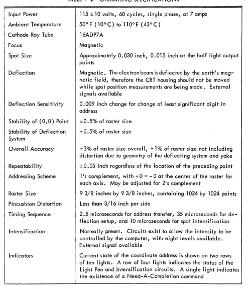
TABLE 1-2 OPERATING SPECIFICATIONS
Input Power
Ambient Temperature
Cathode Ray Tube
Focus
Spot Size
Deflection
Deflection Sensitivity
Stability of (0,0) Point
Stabil ity of Deflection System
Overa II Accuracy
Repeatabi I ity
Addressing Scheme
Raster Size
Pincushion Distortion
Timing Sequence
Intensification
Indicators
115 ± 10 volts, 60 cycles, single phase, at 7 amps
50°F (10°C) to 110°F,(43°C)
16ADP7A
Magnetic
Approximately 0.030 inch, 0.015 inch at the half light output points
Magnetic. The electron beam is deflected by the earthls mag-netic field, therefore the CRT housing shou Id not be moved while spot position measurements are being made. External
signals available .
0.009 inch change for change of least significant digit in address
±0.5% of raster size
±0.5% of raster size
±3% of raster size overall, ± 1% of raster size not including distortion due to geometry of the deflecting system and yoke
±0.05 inch regardless of the location of the preceding point
lis complement, with
+
0 = - 0 at the center of the raster for each axis. May be adjusted for 21s complement
93/8 inches by 93/8 inches, containing 1024 by 1024 points
Less than 3/16 inch per side
2.5 microseconds for address transfer, 35 microseconds for de-flection setup, and 10 microseconds for spot intensification
Normally preset. Circuits exist to allow the intensity to be controlled by the computer, with eight levels available. External signal avai lable
[image:11.615.48.551.73.649.2]CAUTION
An airflow-actuated sail switch controls the application of the 115-volt power to the equipment. Loss of cooling air will shut off
1 - . . 1\.1 J.. J..I • • •• 1 • I • •
tile mam powei. l~eVei opeiCile rrle equIpmenT w:rnour COOling air,
as the deflection ampl ifier transistors wi II overheat. Replacement cost is approximately $600.
I
WARNINGI
SECTION 2
INTERFACE SIGNALS
SIGNAL DESCRIPTION
All logic signals between the computer and the display are either Standard DEC Logic Levels
or Standard DEC Pulses. A Standard DEC Logic Level is either a ground (0 to -0.3 volts) 1
indicated by an open diamond, or -3 volts (-2.5 to -3.5 volts), indicated by a solid diamond.
Aii iogic ieveis appi ied to the conditioning ievei inputs of capacitor-diode gates must be
present for at least 3 microseconds before an input pulse is applied to the gate. The Standard
DEC Pulse is either a positive-going pulse from ground (0 to -0.3 volts) to + 2.5 volts (+ 2.3
to
+
3.0 volts), indicatedby
an open triangle, or a negative-going pulse from ground to -2 .. 5 volts (same tolerances), indicated by a solid triangle; with a pulse width of either 1.0, 0.4,or 0.07 microsecond.
INPUT SIGNALS
Each coordinate address requires a 10-bit binary word composed of Standard DEC Logic Levels.
These levels are -3 volts for logic
0
and ground for logic 1, except for the most-significent bits which are ground for logic0
and -3 volts for logic 1. A 0.4-microsecond pulse isrequired to clear the two Coordinate Buffers in the Type 30, and another 0.4-microsecond
pul.se is required to load the coordinant addresses into the two Buffers. The load pulse must
follow the clear pulse by at least 1 microsecond, and must follow the digital address words by
at least 3 microseconds. Three positive Standard DEC Logic Levels or Pulses are required
if
the intensity level is to be controlled by the computer. These must be received within 33
microseconds after the load pulse occurs. The computer also suppl ies a -1.5 volt level to
light the Need-A-Completion (NAC) indicator.
OUTPUT SIGNALS
Each Coordinate Channel of the Type 30 produces an analog output voltage that varies from
-10 volts to ground directly with the numerical value of the coordinate address word.
produced for 10 microseconds. Forty-five microseconds after the load pulse is received a
O.4-microsecond negative display completed pulse is generated.
If the Light Pen is used and
if
it has seen a spot during the display period, a pulse similar tothe display completed pu Ise wi II be produced. This pu Ise will occur at the same time as the
display completed pulse. In addition, a -3 volt level is produced starting at this time and
SECTION 3
LOGICAL OPERATION
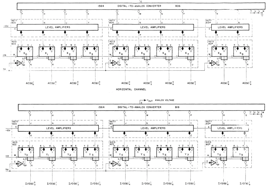
The overall operation of the Type 30 Precision CRT Display can best be understood by
refer-ence to the block diagram, Figure 3-1. The Type 30 uses two channels for horizontal (X-axis)
and vertical (Y-axis) deflection and special control circuitry for timing and intensifying the
spot. The Horizontal and Vertical Coordinate Channels are similar, therefore only one channel
will be described in the discussion to follow. An explanation of the drawing symbology is
given in Section 5 and in the DEC Module Catalog.
HORIZONTAL DEFLECTION CIRCUIT
IO-BIT DIGITAL-TO-ANALOG CONVERTER
IO-BIT HORIZONTAL ADDRESS WORD
LEFT RIGHT
chb
I I
~I ~I
EI
~I
Cl.o o
Cl.
o
...J
Ibp cvb
Fi gure 3-1 Type 30E Block Diagram
VERTICAL DEFLECTION
CIRCUIT
IO-BIT DIGITAL-TO-ANALOG CONVERTER
The coordinate location (address) information for the displayed spot is determined by the
con-tents of two lO-bit binary words, one for the horizontal coordinate and one for the vertical
coordinate. Each word uses the l's complement, in which 1000000000 is -511 or the smallest
number, and 0111111111 is the maximum number, +511. The bits are applied as gating
levels to the two Buffers. When the Type 30 is controlled by DEC's PDP-1 computer, the two
address words are applied in succession by two pairs of memory cycles.
In the next (fifth) memory cycle the computer supplies an 10.1 instruction which causes the
clear and load pulses to
be
ap?1 ied to the Coordinate Transfer Circuit, and usually the threeintensity level bits to the Status and Intensity Circuit. The load pulse causes the two
coordi-nate words to be transferred into the Buffers and starts the display cycle.
During the first 35 microseconds of the display cycle the output of the Buffers is converted into
equivalent analog voltages and applied to separate Deflection Amplifiers through Compensation
Networks. At the end of this time the CRT is unblanked for 10 microseconds and a spot of
light appears on the screen at the location specified by the two coordinate address words.
The intensity of the spot is controlled by the Intensity Bias Circuit.
At the end of the display cycle the Status Circuit generates a negative pulse which is returned
to the computer. A second pulse qnd a negative level wi II also be generated if a Light Pen
has seen the displayed spot.
COORDINATE CHANNELS
Both the Horizontal and Vertical Coordinate Channels are identical, therefore only the
hori-zontal channel will
be
discussed in detail. Figure 3-2 shows a logic block diagram of bothCoordinate Channels.
The information to be displayed occurs as two sets of ten bits, in which ground is a logic 1
and -3 volts is a logic
a
I except for the most-significant bits which are the reverse. Thesebits are applied to the conditioning level inputs of 10 capacitor-diode gates in each Buffer.
Clearing The Buffers - Following the computer instruction that deposits the second coordinate
address word in either the Accumu lator or the In/O ut Reg ister I an 10 T instruction occurs in
the next memory cycle. This lOT instruction causes a negative .slear ~isplay ~ulse (CDP) to occur at tp7. The CDP pulse is ampl ified and standardized by two pulse ampl ifiers in the
-IOV
'b~
-
..
--IOV i
I
i564
1 I
y~---
--- -- _ -.--. _
I
~--
--. -
=- - - -- -
,~--
J
---~----T---·-+-
:
i
I
I
AC(b)~ AC{b}~ AC{b) ~ AC(b)~
1564
K
N y
LEVEL AMPLIFIERS
' .
I~-
- - -~---I~---I I i
---,--- - - - --i- - - - -
-1--1
I ' I I
(4213 - - -
1- -.
I B22 H J HI J
cvb
I
I/O(b) ~",-r-"_K~L~ W X W X Y Z y, Z I I I I I I/O{b) : I I
-r---~-J
.
I
: 1
i I
I I
I/O{b) ~ I/O(b)~
~ XOUT ANALOG VOLTAGE
E
DIGITAL -TO-ANALOG CONVERTER B06
1
~ ~ ~ ~ ---i---:---I~~
~
~
- - - IJ IN lu Iy
i
LEVEL AMPLIFIERS
1
I
R T U I
i - -
----1--- -
~_Ji
I
AC(b) ~ AC(b) ~ HORIZONTAL CHANNEL
i I
I
1AC(b) ~
I
AC{b) ~
YOUT ANALOG VOLTAGE
E
DIGITAL-TO-ANALOG CONVERTER BI9
~
---
~
---
---I~
--
----I~-,
J N U l Y i
LEVEL AMPLIFIERS
! I
L - - -
-I
~
- - - (- - - -
i~
- - --i~
-
JI ! ' ,
~iI3-
-
1 - - -- --1- - - 1- - - - -
-1--'
I H J H J K L K; L W X W X y Z y: Z :
I <
I Vo
1M
I SM~_+_r---~~~~---~~4_+_---~~_+~
~
IE~
I [:Yt9Pl'
N"
I
RI
L _ _ _ _ ( _ _ _ _ _I ______
---1---i
I
I
I ,
I/O{b) ~ I/O(b) ~ IIO b) ~ I/O(b) ~
VERTICAL CHANNEL
'_"->M X,
AC(b) ~
14677-- - 1, .. .. -j8i3* I U
1 E
1
1
AC(b) ~
'-'-,
y
L
IV- - - : - - - '
M
I s~~~-+---~-*-~
'
liE E~ p~
Fi
l~p
, L"
IIO b) ~
!
I
I
I/O/b) ~
[image:18.1229.162.1089.67.707.2]Coordinate Transfer Circuit, becoming the positive ~Iear ~orizontal ~uffer (chb) and .:,Iear
~ertical ~uffer {cvb} pulses. These pulses are appl ied to the direct clear inputs of all the flip-flops in the Buffers and the Status and Intensity Circuit, setting them to their ZERO (or
ONE) states. The Horizontal Buffer now holds 0111111111
(+
511) and the Vertical Buffernow holds 1000000000 (-511). However, each flip-flop in the Horizontal Buffer produces a
-3 volt output while each flip-flop in the Vertical Buffer produces a ground output, due to
the reversal of the most-significant bits definition.
Loading the Buffers - In either the same or next succeeding lOT instructions, a negative Load
pisplay ~ulse (LDP) occurs at tp10. This pulse is also amplified and standardized by a pulse amplifier in the Coordinate Transfer Circuit, and becomes the negative 0ad !:uffer £:ulse (Ibp).
The Ibp pulse is applied to five pulse inverters, producing positive .!!"igger £Iate £:ulses (tgp)
that are appl ied to the trigger inputs of the 10 capac itor-diode gates in each Buffer.
Each bit in the horizontal address word which is a logic
0
(except the most-significant bitwhich would be a logic 1) and each bit in the vertical address word that is a logic 1 (except
the most-significant bit which would be a logic O)will apply a ground potential to the
con-ditioning level input of its capacitor-diode gate for at least three microseconds before the
LDP pulse occurs. This enables the gate and causes it to differentiate the tgp pulses. The
positive signals which result are applied to the associated flip-flops, complementing them to
their opposite states.
Those bits of the address words which are -3 volts disable the capacitor-diode gates and prevent
the flip-flops from being complemented by the tgp pulses. Therefore at the completion of the
LDP pulse each fl ip-flop in the Horizontal and Vertical Buffer has been set to the same state
as the corresponding fl ip-flop in the computer's AC and I/O Registers.
Digital-to-Analog Conversion - Each 10-bit coordinate address word is converted into an
analog voltage by a resistive-ladder network in a Type 1564 module. This analog voltage
varies its upper and lower I imits in 1024 discrete intervals, and is directly proportional to the
numerical value of the 10-bit binary word from the Buffer. The upper and lower voltage
I imits are set by the two voltage levels of the ten input bits to the D-A Converter. The lower
voltage is set at -10 volts, and is determined by a stable Type 1562 Reference Voltage Supply
module. This voltage is appl ied to the ten Level Amplifiers, each of which apply it to the
obtained by saturating the Level Ampl ifier. This makes each discrete interval equal to
approxi-mately 10 millivolts.
The output of each Buffer is ten bits, each at =3 volts when the Buffer holds 0111111111
(+
511,holds 1000000000 (-511, Horizontal Buffer complemented and Vertical Buffer cleared). This is
a 10-bit binary word in which ground is logic
0
and -3 volts is a logic 1.Each Level Ampl ifier is cut off when its input is at ground and is saturated when its input is at
-3 volts. Therefore the analog voltage is ground, its most positive value, when the Buffer
holds
+
511 and is -10 volts .. its most negative value, when the Buffer holds -511. This repre-sents deflection to the extreme top or right-hand side, and to the extreme bottom or left-handside, respectively. Table 3-1 shows the relationships between the coordinate address words,
fl ip-flop states, D-A conversion, and deflection.
TABLE 3-1 COORDINATE CHANNEL LOGIC CONVERSION TABLE
Diaital Address Buffer Outout
I
Level Amol ifier OutoutI
Diaital-to-Analoa""
.
, - I V v,
and and and Converter
FI
ip-Flop States Level Amplifier Input D-A Converter Input Output ;I
' f
0111111111
I
xxxxxxxxxxI
0000000000I
most positive ~0111111110 xxxxxxxxxO OOOOOOOOOX
I
(ground)
·
·
·
·
·
·
·
·
·
·
·
·
·
·
·
·
·
·
0000000001 xOOOOOOOOx OXXXXXXXX 0
·
·
!
I
I
·
0000000000 xOOOOOOOOO OXXXXXXXXX
·
·
I
·
1111111111 Oxxxxxxxxx XOOOOOOOOO
·
·
I
·
1111111110 OxxxxxxxxO XOOOOOOOOX
·
I
I
·
·
·
·
·
·
·
·
·
·
·
I
·
I
·
·
·
·
·
I
·
1000000001 OOOOOOOOOx XXXXXXXXXO
i
·
most negative i
1000000000 0000000000 XXXXXXXXXX ! i (-10 vol ts)
t
o
== logic zeroo
== groundo
== ground i i Posi tive=
up=
ZERO state x= -
3 voltsI
X=
-10 volts=
right1 == logic one
,
Ii
Nego
ti ve=
down== ONE state
side, respectively. Table
3-1
shows the relationships between the coordinate address words,flip-flop states, D-A conversion, and deflection.
The accuracy, or linearity, of the analog address voltage with the coordinate address is
deter-mined by the D-A Converter adjustment, and is approximately ±l millivolt per bit. This
adjustment is necessary to correct for the sl ight resistance differences of the resistive ladder
network and the saturation resistance of each Level Amplifier. If any part of a resistive ladder
network or a Level Ampl ifier is changed, the D-A Converter must be readjusted as described in
Section
4.
The value of the analog address voltage will not reach its final value for approximately
2
microseconds after the LOP pulse occurs. This is due to the delays in the pulse amplifiers, the
flip-flops, the Level Amplifiers, and the ladder networks. This time is part of the deflection
setup delay, which also includes the compensation time. The analog address voltage is avai
1-able at a BNC connector for external use, along with the reference voltage for preamplifier.
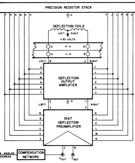
DEFLECTION CIRCUITS
Both the Horizontal and Vertical Deflection Circuits are identical, therefore the description
that follows applies equally to both circuits. Figure
3-3
shows the logic diagram for thesecircuits.
Basically, the Deflection Circuit consists of a Compensation Network, a Deflection
Preampli-fier, a Deflection Output Amplifier with a stack of associated Precision Resistors, a Reversing
Switch (in the Type 30M only), and a pair of Deflection Coils. The electron beam is
de-flected by a magnetic field produced by the dc currents flowing in the two opposing Deflection
Coils. This circuit acts as a stable and linear operational amplifier, permitting the
compen-sation needed for correction of the yokels undershoot to be introduced at the inputs.
Compensating - When the coordinate address is changed, a voltage step is produced in the
analog address voltage. Since abrupt changes of the current in the Deflection Coils would
produce ringing and the spot would oscillate, the Deflection Coils are damped. The amount
of damping used is sl ightly less than critical in order to minimize the deflection setup delay
R N M K H
j
i
I I
I I
I I II I I
H
K
PRECISION RESISTOR STACK
_ 0 F J L P S U
DEFLECTION COILS
+~O VOLTS
P-4
J-4
I
I
I I I
F
J
II1II
~I
DEFLECTION
OUTPUT
AMPLIFIER
I~
11111
LEFT
R
s
T
u
z
y
..Lo
1567
DEFLECTION
PREAMPLIFIER
y
RIGHT
F
H
J
K
L
~---:~.~~:---~
z
w
X ANALOG
COMPENSATION ___
---~..
t\ADDRESS
NETWORK
~'!Ix
OUTFigure 3-3 Deflection Circuit Block Diagram
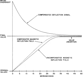
An abrupt voltage change to the Defiection Preampi ifier does not cause an abrupt change in
the deflection current due to the large inductance of the Deflection Coils. Instead, the current
[image:22.618.85.549.51.612.2]Figure 3-4. Because of the coupl ing between the Focus Coi I and Deflection Coi Is and the
hysteresis of the paramagnetic items in close proximity to the coils, the magnetic field does
not completely stabilize at its final value. For about 150 microseconds after the change of
address, a slightly uncertain undershoot value exists that is a little less than the required
value. Therefore a Compensation Network is used to introduce some initial overshoot into
the coordinate address change.
The Compensation Network is a simple RC circuit with a time constant of about O. 1
milli-second that appl ies a signal to the preampl ifier which is initially much greater than required
and which decreases exponentially toward that value. This overshoot causes the magnetic
field to approximately reach its required val ue by the end of the 35-microsecond deflection
setup delay. The overshoot is a fixed percentage, wh i Ie the undershoot varies somewhat
depending upon the previous address; therefore the compensation is not exactly complete.
However, with proper adjustment of the Compensation Network, the resulting spot move-ment wi II be negl igible for most appl ications.
Amplifying - The compensated analog address voltage is applied to terminal Z of the
Deflec-tion Preamplifier, and a stable -10 volts is applied to terminal P. This latter potential is
divided in half to produce a -5 volt reference voltage, available as X
REF at terminal W. These two vol tages are the inputs to a differentia I ampl ifier.
INITIAL OVERSHOOT
/COMPENSATEO OEFLECTION SIGNAL
~~~~--~---.··~·~~~~==~t=====
COMPENSATED MAGNETIC.· VALUE
[image:23.612.158.430.437.689.2]DEFLECTION FIELD ~... UNCERTAIN
...
~UNCOMPENSATEO
MAGNETIC DEFLECTION FIELD~~~~L-4~-+---+--~--~--4---+---+---~~---+
o 5 10 15 20 25 30 35 40 45 50
MICROSECONDS
The differential amplifier compares the analog voltage with the reference voltage and
pro-duces two outputs which are proportional to the difference between the two inputs. Both of
these outputs vary from a common reference potential (approximately +4 volts) by the same
amount but in different directions, one going positive whiie the other goes negative.
signal controlling the conduction through a separate amplifier channel. The deflection
current flows through a stack of Precision Resistors, the amplifier channel, and Deflection
Coil. The Precision Resistors develop a negative feedback voltage that is applied to the
Preampiifier to increase the stabiiity of the circuit. The Defiection Output Ampiifier and
Precision Resistor Stack utilize forced air for cooling. Zener diodes across the Deflection
Coils prevent the back emf developed by changing an address from burning out a Deflection
Output Ampl ifier.
NOTE: Loss of cool ing air wi
II
resul t in burning up an expensive assembly. Never operate the equipment if the fans or sail switch,. e.
ra II.
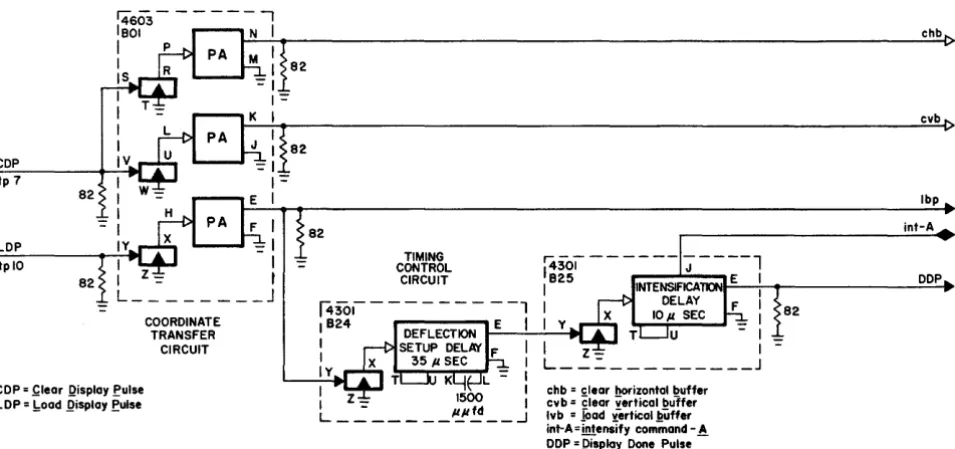
CONTROL AND TiMING CIRCUIT
The Control and Timing Circuit consists of the Coordinate Transfer Circuit and the Timing
Con-trol Circuit, shown in Figure 3-5. The Coordinate Transfer Circuit generates the pulses which
clear and load the Buffers and the Status and Intensity Circuit, as well as initiating the Timing
Control Circuit's operation.
Coordinate Transfer Circuit
Clear Pulses - When the computer wants to clear the Buffer, it applies a ~Iear Qisplay Pulse (CDP) at tp7 to two inverters in a Type 4603 Pulse Amplifier module. The inverters then
con-duct and activate two pulse ampl ifiers, producing positive ~Iear .b.,orizontal ~uffer (chb) and
~Iear ~ertical ~uffer (cvb) pu Ises which are appl ied to the fl ip-flops in the Hori zonto I and Vertical Buffers. The cvb pulse is also applied to the flip-flops in the Status and Intensity
Circuit. The clear pulses are divided in order to provide the required driving power for the
large number of flip-flops. Each pulse clears 12 flip-flops, the chb pulse also clearing the
COP tp 7
LOP tplO
COP = ~Iear Qisplay pulse LOP = boad Qisplay pulse
COORDINATE TRANSFER
CIRCUIT
Figure 3-5
82
TIMING CONTROL
CIRCUIT
chb = clear horizontal buffer cvb = clear vertical buffer Ivb = lOad ~ertical ~ffer
int-A = mtensify command -~
DDP = Qisplay Qone pulse
82
Control and Timing Circuit Logic Block Diagram
chb
cvb
Ibp
int-A
DDP
Load Pulse - Approximately 2.2 microseconds after the CDP pulse, the computer supplies a
!:oadQisplay ~ulse (LDP)attp10. This pulse is also applied to an inverter in the Type 4603 Pulse Amplifier module, causing the inverter to conduct and activate a pulse amplifier which
produces a negative !.oad !:uffer £ulse (Ibp). This pulse is applied to the pulse inverters in
both Buffers (causing the coordinate address words to be loaded into the Buffers) and to the
Timing Control Circuit (initiating the display cycle).
Timing Control Circuit
The Ibp pulse is applied to an inverter in a Type 4301 Delay module, producing a positive
pulse that initiates the 35-microsecond deflection setup delay period. While the Deflection
Setup Delay is timing out the coordinate address words are loaded into the Buffers, converted
into equivalent analog voltages, and develop currents to deflect the electron beam. The
length of time is determined by the transfer time of the Buffers, D-A conversion time, response
time of the amplifiers, and primarily the characteristic time of the Deflection Coils and
[image:25.615.64.542.95.320.2]At the end of the 35-microsecond period the Deflection Setup Delay produces a negative
pulse that is applied to an inverter in another Type 4301 Deiay module. Againj the inverter
conducts and initiates a la-microsecond intensify delay. While the Intensification Delay is
timing out a - 3 volt intensify-A (int-A) level is produced which causes the Intensity Bias
Cir-cuit to unblank the CRT. At the end of the la-microsecond period a negative Display Done
Pulse (DDP) is produced and returned to the computer. The DDP pulse is also used by the Status
and Intensity Circuit to produce a pulse and light an indicator if the Light Pen saw the pulse.
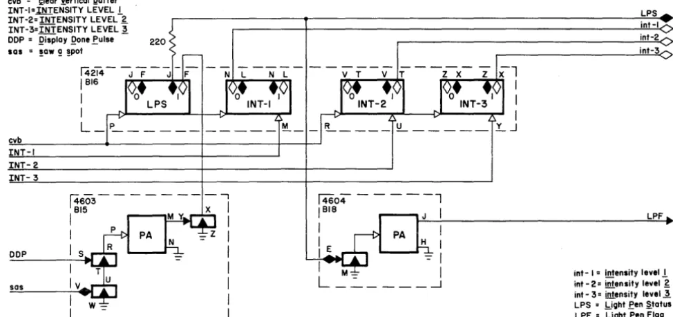
STATUS AND INTENSITY CIRCUIT
The Status and Intensity Circuit shown in Figure 3-6 generates a negative pulse and level and
iights an indicator when the Light Pen sees the displayed spot. The circuit also contains the
Intensity Buffer that selects the intensity level of the displayed spot. Because the four
f!ip-flops are cleared by the cvb pulse each time a CDP command occurs, the Intensity Buffer must
be reloaded before the end of the deflection setup delay.
cvb = !;.Iear yertical Ruffer INT-I=.IrITENSITY LEVEL! INT-2=INTENSITY LEVEL 2 INT-3=INTENSITY LEVEL "3
DDP = Qisplay Qone fulse
-sas = !aw!! !pot
cvb INT-! INT-2 INT- 3
~603-- - - ' I
815 X
I M ~ I
I I
~DD~P ______ I~s~
=
I
I
I
sas I V
I
=---~
I w _ I
L_-=- _______
--.Jf"4604 - - - l
~:
I H IIE -::- I
I M _ I
L_~
____
..JFigure 3-6 Status and Intensity Circuit Logic Block Diagram
LPS int-I int-2 int-3
int-I = intensity leve' I int-2= i.!iiensity level
g
int - 3 = intensity level ~LPS = !,Jc;Jht fen §.tatus LPF = bight fen Elac;J
Light Pen Status - At the end of eCich
display
cycle a negative ,Qisplay Qone !uise (DDP) isapplied to an inverter gate in a Type 4603 Pulse Amplifier module. This inverter gate is
con-trolled by another inverter which receives the light pen gate signal. When a Type 32 Light
[image:26.618.73.560.377.606.2]duri ng and~sl
ightly
after the spot's display period. This turns on the inverter, enabl ing the inverter gate and allowing the DDP pulse to activate the pulse amplifier. The pulse amplifierturns on a third inverter which complements the light Pen Status Flip-Flop, thereby producing
a negative .!:.ight ~en ~tatus (LPS) level that is returned to the computer.
The LPS level is also applied to another inverter in a Type 4604 module which conducts and
activates a pulse amplifier. This pulse amplifier produces the positive .!:.ight ~en ~Iag (LPF)
which is returned to the computer.
Intensity Buffer - Eight different levels of intensity are possible with the Type 30. These levels
correspond with the numerical value of a 3-bit l's complement binary word supplied by the
com-puter. The Intensity Buffer stores this word from its appl ication til the next CDP command occurs.
The intensity word must be appliedwithin33microseconds after the LDP command occurs to allow
the intensity bias to be set before the deflection setup delay ends. Table 3-2 shows the
cor-relation between the intensity word, flip-flop states and outputs, and relative
.int~nsity
·Ievels.The flip-flops are changed from their ZERO state to their ONE state by the application of a
+
2.5 vol t pulse (or level). Since the most-significant bit in the intensity word is reversed,the output of the fl ip-flop is also reversed. This allows the intensity to automatica lIy be set
just above the median level if no input signal is received.
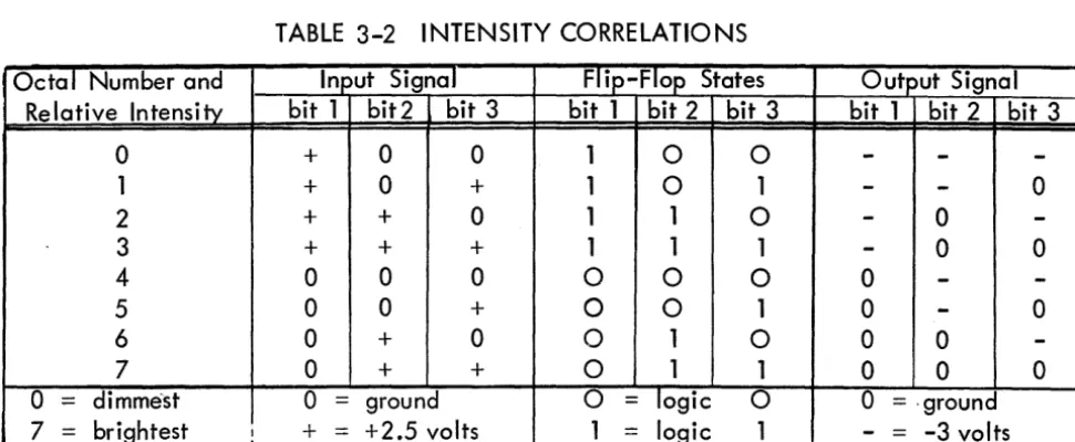
TABLE 3-2 INTENSITY CORRELATIONS
Octo I Number and Input Signal Flip-Flop States Output Signal Relative Intensity bit 1 bit2 bit 3 bit 1 bit 2 bit 3 bit 1 bit 2 bit 3
0
+
0 01
0
0
-
-
-1
+
0+
1
0
1
-
-
02
+
+
01
1
0
-
0-3
+
+
+
1
1
1
-
0 04
0 0 00
0
0
0-
-5 0 0
+
0
0
1
0-
06 0
+
00
1
0
0 0-7
0+
+
0
1
1 0 0 00 ;::: dimmest 0
=
ground0
=
logic0
0=
·ground [image:27.620.63.549.484.684.2]INTENSITY BIAS CIRCUIT
The Intensity Bias Circuit, Figure 3-7, is located in the CRT housing. It includes a Type 1705
Bias and Focus module and a Type 4688 Variable Amplitude Intensifier module. These modulesj
along with a Type 1559 Light Pen Amplifier and any other that may be in the spare socket,
constitute level D for location purposes.
Intensifying - While the Intensification Delay is tim-ing out, the negative int-A signal is
applied to a negative NOR gate in a Type 4688 Variable Amplitude Intensifier module. This
turns on a variable intensity bias circuit, whose output, the INTensity
(tNT)
command is accoupled to the cathode of the CRT. Normally the INT signal is at ground, but during the
10-microsecond intensification delay period it goes to some value between -20 and -35 volts,
depending on the intensity level inputs. This reduces the bias and unblanks the CRT, allowing
a spot of light to appear on the screen at the coordinate location specified by the two address
words_.
int-A R
int-I
int-2
int-3
4688 D03
VARIABLE INTENSITY BIAS
CIRCUIT
z oe
de y
( ; ) J 1 4
"f-/
Z AXIS : INT,.., -80V
+200V
CATHODE
GRID I
GRID2
6.3 VAC FOR
j-Y X T FILAMENT
\c---f
1705 D02
v
CRT BIAS
, - - - ' < - f VOLTAGE DIVIDERS !-'-H-'---_ _ _ _ -l( FOCUS 2
E D
Figure 3-7 Intensity Bias Circuit Logic Block Diagram
S-IO
J-7
Intensity Levels - The dc bias potentials for the CRT grids are developed in the Bias and Focus
module by Zener diode voltage dividers. Grid 2 is kept at +200 volts, while grid 1 is normally
kept at approximateiy -80 volts. The latter potential can be adjusted from 0 to -120 volts to
adjust the intensity level. Two diodes connect the cathode to the grid so that the cathode can
CAUTION
Repeated and/or intensely bright intensifications can burn a hole in the screen of the CRT, ruining an expensive tube.
When the CRT is blanked the cathode is at ground. In order to unblank the CRT and produce
a spot of light, it is necessary to apply a - 3 volt enabl ing potentia I to anyone of the six NOR
inputs. This potential turns on an inverter which enables the variable intensity bias circuit.
The INT signal is capacitively coupled to avoid ruining the CRT in the event of a malfunction.
A Z axis BNC connector makes the INT signal avai lable for external use.
The intensity bias circuit is capable of providing 16 different potentials for the cathode,
depending on the binary number present on terminals F,
J,
U, and X. The Type 30 uses onlythe three less-significant bits of this number, providing eight intensity levels. When the
number is 7 (all grounds), the cathode potential is -35 volts and a bright spot is displayed.
When the number is 0 (all -3 volts) the cathode potential is about -20 volts, giving a dim
spot.
Focus - The CRT is focused magnetically by a constant current through a Focus Coil. This
current is controlled by a focus transistor, Q 1, which in turn is controlled by a fixed voltage
from the Type 1705 Bias and Focus module '$ focus voltage divider. A potentiometer allows
the current in the focus transistor to be adjusted if necessary.
INDICATORS CIRCUIT
Twenty-five incandescent lamps are used in the indicator panel. All but one of these indicate
the state of various flip-flops in the equipment, glowing when the flip-flop holds a ONE and
dark when the
fI
ip-flop holds a ZERO. The exception is the Need A ~ompletion (NAC) in-dicator which is lighted when the computer requests a signal at the end of the display process.This lamp is energized directly by - 15 volts from the computer.
All the other lamps are energized by -15 volts from an indicator driver. Nine of these are
contained in each driver module, and each one is actuated by a -3 volt signal from the 1
ELECTRICAL POWER
The primary power for the equipment is 115 volts, 60 cycles, single phase. This is applied to
a 20 am Pi 2 pole circuit breaker located on the Type 811 Power Control panel. From the
circuit breaker the 115 volt power goes to the ac power control circuit, to the cooling fans,
and through the contac ts of re lay K 1 to the dc power suppl ies.
One side of the ac line from the circuit breaker goes to the coil of K1 and to the cooling fan
motors. The other side of the ac line goes to the normaiiy-open contact of an airflow-actuated
sail switch (operated by the central cooling fan) and to contacts on relay K2. When K2
is energized, the cooling fans are energized. When the fans come to speed, the sail switch
wi II close and relay K 1 wi II be energized, thereby applying the ac power to the dc power
suppl ies.
The ac power from relay K1 is applied to the Type 722 Power Supply. An outlet on the Type
722 supplies the ac power to the Type 770 Power Supply. Similarly, the Type 770 supplies
.1 • .= iii.. ; Ir- r-~n ,n , ii""'t. ,.. I
me ac power TO Tne I"\IJt t\..XK OU-O t'ower :>upply.
NOTE: Some equipments may use a Type 721 Power Supply instead of a Type 722.
The Type 722 (or Type 721) Power Supply provides the + 10 volts and -15 volts DC for the
logic circuits. Refer to the DEC Module Catalog for complete specifications.
The Type 770 Power Supply provides the high voltage and filament power for the CRT e Its
outputs include + 10,000 volts DC, +250 volts DC, -150 volts DC, and 6.3 volts AC.
I
WARNING
I
Lethal voltages are present when the Type 770 Power Supply is energized. Exercise extreme caution working inside the equ ip-ment when it is turned on. The black ring around the CRT near the front bezel ( exposed on early models) must never be touched or closely approached with power on.
The Modei EQR 60-6 Power Suppiy provides the 50 voit defiection power for the CRT yoke.
NOTE: If the individual power suppl ies are turned on and off separately I be sure that the EQR 60-6 Power Supply is not turned
on when the Type 722 is turned off. If the EQR 60-6 is used without the Type 722, it will overconduct and to into its
current-limiting mode.
SECTION 4
MA I NTE NANCE
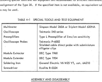
SPECIAL TOOLS AND TEST EQUIPMENT
The following special tools and test equipment are recommended for efficient maintenance
and realignment of the Type 30. If the specified item is not avaiiabie, an equivaient
sub-TABLE 4-1 SPECIAL TOOLS AND TEST EQUIPMENT
tv\ultimeter Simpson /v\odel 260A or Triplett ti\odel 630NA
Osc ill oscope T ek tron ix 540 seri es
Preamplifiers Type L Preamplifier of 5 mv/cm sensitivity
Oscilloscope Probes Tektronix P-6002
Module Extractor
Module Extender
Soldering Iron
Screwdr i ver
Shielded cable direct probe with subminiature a
II
i ga tor c lipsDEC Type 1960
DEC Type 1954
General Electric V6 W25 VT, cat. 6A210
Xcel ite R-3324
ASSEMBL V AND DISASSEMBL V
Logic Modules - All logic modules may be easily removed by unplugging them from their racks.
Access to the modules is gained by opening the rear door of bay 2. A Type 1960 Module
Ex-tractor shou Id be used when removing any logic modu Ie.
NOTE: When removing or replacing a module, be sure all power is turned off.
Deflection Output Amplifier - The resistor stacks and the deflection output amplifier heat sink
assembly may be unplugged after the 11 O-vol t power to the fans has been removed. Two
[image:32.615.98.530.199.544.2]heat sink can be removed. The resistor stacks must be removed before the heat sink module
can be removed.
Cathode Ray Tube - The front bezel and the CRT mounting assembly that holds the yoke and
focus coil must be removed from the bottom of the shroud by unscrewing the four underneath
hold-down screws (two at the bezel and two at the rear of the assembly) and the two screws
that hold the mounting assembly to the sides of the shroud. Once removed, the assembly
should be set up on blocks with the CRT face down and the four bolts that hold the CRT
mount-ing assembly to the bezel removed. The yoke and focus coil assembly is removed by
unscrew-ing the three bolts that sprunscrew-ing-load it on the CRT mountunscrew-ing assembly. The CRT is removed by
loosening the screws which hold the clamps that secure the tube to the front bezel. The CRT
mounting assembly can then be removed from the front bezel.
To replace the tube, place it face down on the plexiglass shield in the bezel. Place the CRT
mounting assembly over the tube and bolt it down. Place the yoke assembly very carefully
over the tube and bolt it down. Place the yoke assembly very carefully over the neck of the
tube, and at the same time al ign the tube with the yoke. When the tube has been al igned,
it should be possible to move the yoke back and forth without scraping the neck of the tube.
Next, tighten down the tube clamps. Then install the hold-down screws for the yoke and focus
coil assembly.
ADJUSTMENTS
Light Pen Gain - Located underneath the right front of the CRT housing. Clockwise rotation
increases
ga
in.Electrical Adjustment
Digital-to-Analog Converters - If any level amplifiers in either the Horizontal or Vertical
Deflection Channels have their output transistors replaced, or if the module itself is replaced,
the Digital-to-Analog Converters associated with that channel will have to be adjusted. The
procedure for adjusting these D-A Converters is as follows:
(a) Turn off the main ac power to the Type 30.
1954 Module Extender into the space in the rack, and then replace the D-A
Converter in the extender.
(c) Remove the Type 1567 Deflection Preampl ifier associated with the D-A
Converter being adjusted.
(d) Individuaily turn off the Deflection and Ultor Voltage Power Supplies (EQR
and Type 770). The main ac power may now be turned on.
(e) Program the computer to
01
ternotely display the most negative number(0000000000) and the next less negative number (0000000001 ). This will
alternately switch the least significant digit (bit 9) between its two states.
Refer to Tables 3-1 and 4-2 for computer and converter states.
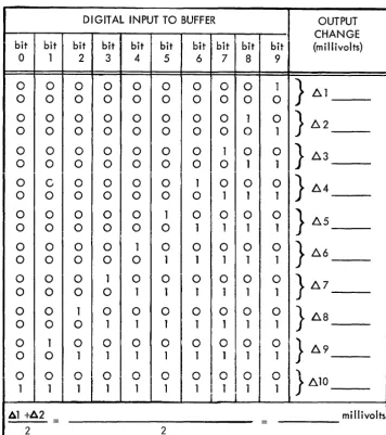
TABLE 4-2 10-BIT DIGITAL-TO-ANALOG CONVERTER ADJUSTMENT
DIGITAL INPUT TO BUFFER
bit bit bit bit bit bit bit bit bit
0 1 2 3 4 5 6 7 8
0 0 0 0 0 0 0 0 0
0 0 0 0 0 0 0 0 0
0 0 0 0 0 0 0 0 1
0 0 0 0 0 0 0 0 0
0 0 0 0 0 0 0 1 0
0 0 0 0 0 0 0 0 1
0 C 0 0 0 0 1 0 0
0 0 0 0 0 0 0 1 1
0 0 0 0 0 1 0 0 0
0 0 0 0 0 0 1 1 1
0 0 0 0 1 0 0 0 0
0 0 0 0 0 1 1 1 1
0 0 0 1 0 0 0 0 0
0 0 0 0 1 1 1 1 1
0 0 1 0 0 0 0 0 0
0 0 0 1 1 1 1 1 1
0 1 0 0 0 0 0 0 0
0 0 1 1 1 1 1 1 1
I
0
~I
0 0 0 f"'\I
f"'\ '"' ' " ' !-
-
1-,-1
1 1 1 1 1 1
I
1 I 1 fA1 +A2
=
2 2
bit 9 1 0 0 1 0 1 0 1 0 1 0 1 0 1 0 1 0 1
'"'
-
1=
OUTPUT CHANGE (millivolts)} 81
}M
} 83
}
.6.4}
.6.5} 86
} 87
} 88
}M
"\
j
.6.10 [image:34.617.138.495.332.733.2](f) Connect the direct probe from the horizontal input of the osci IIoscope to
terminal E of the module being adjusted. Set the oscilloscope for 5 mv/cm
vertical dc sensitivity and internal sync.
(g) Adjust the oscilloscope time base so that two horizontal lines appear on the
screen. Measure the vol tage difference of these two I ines as well as possible and
record this value as 11 1 (see Table 4-2). This voltage should be approximately
10 mill ivolts.
(h) Program the computer to alternately switch the next less significant digit
(bit 8). Measure the difference of the two horizontal lines and record this
value as 11 2.
(i)
Add the values of 11 1 and A 2, and divide by 2 to obtain the average change
per bit. Record this value. These bits are not adjustable, and the differences
BIT
7
BIT 6
-BIT
5
-BIT
4 .
-BIT 3
-BIT
2 - - - -
...
BIT 1
-BIT O---~
between them are caused by the sl ight differences in tolerances in both the D-A
converter and the level amplifier output transistors. If these two values are not
close
(±
1 millivolt), check both circuits for a malfunction.(j) Program the computer to alternately switch bit 7 and bits
8
and9,
and notethe voltage difference of the two lines. If this voltage is different from the
average value of the unadjustable bits, adjust the potentiometer behind the hole
nearest the plug end of the module. See Figure 4-1 for the adjustment locations.
(k) Repeat step
(j)
for each bit in turn. Each bit must be adjusted for the samevalue.
NOTE: Ifanybitcannot be adjusted, especiaily the more signif-icant bits, it is necessary to assume a slightly different value for the average of
ll.
1+
A.2; then readjust all the adjustable bits in turn for this value.Raster Position - The raster should be located in the center of the CRT screen. If it is not, it
may be moved by the following procedure:
(a) Program the computer to display vertical and horizontal lines along each
edge of the raster.
(b) Adjust potentiometer R2 (center hole, Figure 4-2, in the Type 1567 module
located in B17) to center the vertical lines.
(c) Adjust potentiometer R2 in the Type 1567 module in location B08 to center
the horizontal lines.
Raster Size - The size of the raster on the face of the CRT should be nine and three-eighths
inches per side. It may only be adjusted after the raster is centered. The raster size is adjusted
in the following manner:
(a) Program the computer to al ternately display the most positive and most
neg-ative horizontal lines (see Table 3-1). Measure the distance betvveen these lines
at their center.
(b) Adjust potentiometer R16 (lower hole, Figure 4-2) in the Type 1567 module
located in B17 for nine and three-eighths inches between the midpoints of the
- - - - R I 6
- - - R 2 - - - R I 7
Figure 4-2 Type 1567 Adjustment Locations
(c) Program the computer to alternately display the most positive and most neg-ative vertical lines. Measure the distance between these lines at their center.
(d) Adjust potentiometer R16 in the Type 1567 module located in B08 for nine and three-eighths inches spacing between the midpoints of the two vertical lines. Common Mode - If a Type 1567 Deflection Preampl ifier module is replaced, it may be neces-sary to adjust its common mode current. This may be done by the following procedure:
(a) Program the computer to alternately display the most positive and most neg-ative addresses in both the horizontal and vertical positions at the dimmest intensity
level.
(c) If the voltage range is greater than this, adjust potentiometer R17 (upper
hole, Figure 4-2) so that the lower voltage is 0.5 volts minimum.
CAUTION
If
the higher voltage range is too great (approximately +7 volts), the deflection ampl ifiers may be burned up.Brightness - The relative brightness of
all
displayed intensity levels is controlled by the cathode-to-grid1
bias. To vary the relative brightness, the following procedure is used:(a) Program the computei to display eight separate iines on the CRT, each line at
a different intensity level.
(b) Adjust the bias control potentiometer R3 (lowest control) on the Type 1705
module in D02 for the best levels of intensity.
CAUTION
Reducing the grid bias by too great an amount will produce an ex-tremely bright spot on the screen of the CRT, which can burn a hole in the screen.
Delay Time - The variable delay of the Type 4301 modules may be adjusted as follows:
(a) Connect an oscilloscope (set for dc input and negative internal sync) to
terminal
J
of the module to be adjusted.(b) Trigger the delay with the program or by connecting a 0.01 microfarad
capacitor (which has previously been shorted) between terminal X and ground.
A -3 volt level should be observed for the required duration.
(c) To change the duration of the delay I adjust potentiometer R7 through the
access hole in the back of the module.
(d) With the oscilloscope adjusted to be triggered with the delay trigger,
con-nect the probe to term ina I E and check for a - 3 vol t pu Ise starting at the end
of the delay period.
(a) Program the computer to display the two alternate diagonals on the screen
of the CRT. Observe the focus along each I ine, especially at the corners and
the center.
(b) Adjust potentiometer R5 (bottom rear) in the Type 1705 module in D02 for
the best focus over the entire tube face. If astigmatism is present, adjust the
a Ii gnment of the Focus Coi I.
Mechanical Adjustments
Focus Coi I - The focus coi I may be moved in any direction by the adjusting screws provided.
It
can move in or out, tilt in either direction, and move sideways.It
should require adjust-ment only when a CRT has been replaced. In order to align the focus coil correctly, the shortbrown jumper on the mounting plate in the bottom of the CRT housing should be removed and
a sinusoidal signal (such as that obtained from an audio oscillator) connected in its place.
This will cause the focus current to vary rapid Iy, focusing and defocusing the spot so that the
concentricity of the focused and defocused spot can be observed. When the coi I is perfectly
aligned, the focused and defocused spots should be perfectly concentric. There should be no
circular motion as the spot changes from its unfocused to focused condition. The coil need
not be perfectly aligned for most applications.
Deflection Yoke - The deflection yoke adjustment affects only the angular position of the
display on the tube face. The three aluminum clamps holding the yoke may be loosened to
rotate the display. It should only require adjustment when the CRT has been removed.
PERIODIC MAINTENANCE
Clean the Rotron fan filters in the deflection and focus output amplifiers once a month with
soapy water. Spray with Fi Iter-Kote (Research Products Corporation, Madison, Wisconsin)
or equivalent.
Clean dust from the Deflection Output Amplifier Heat Sink and Resistor Stacks once every six
months.
Check accuracy of ladder decoder alignment as desired. These should require readjustment
only when a level amplifier module is replaced, or once every six months. See decoder
Refer to the NJE manual for maintenance requirements of the EQR 60-6 power supply.
TROUBLESHOOTING
An understanding of operation of the equipment as described in Section 2 should allow many
maifunctions to be isoiated to a particuiar circuit or component. Further isoiation may then
be accomplished with the schematic diagrams in Section
5.
When troubles do occur, it ismost advantageous to trace each signal path from input to output and compare the signals
observed with the Standard DEC Signal for both shape and timing.
Some of the possible malfunctions do not lie in the logic circuitry and cannot be found by the
standard deductive process. Those pecul iar malfunctions wh ich affect the beam are
I
isted inTable 4-3 below.
i
!
I
I
I
TABLE 4-3 POSSIBLE CRT BEAM MALFUNCTIONS
Symptom
Beam deflects over one
ha If axis only.
Some locations on tube
face cannot be addressed,
i . e. , missing spots in a
line.
Ripple,
ji
tter, or other si ze changes that occurat edges of screen but
~ 1.
not In (.;enier.
Spots appear elongated.
Trouble is most apparent
when two successive
points are widely separated.
I
Probable Cause
Possible shorted Deflection Output Amplifier transistor
i
(2N1719) or open lead in deflection yoke cable.
i
Check Buffer Register, Level Amplifiers and Decoder
adjustments for the axis involved.
Defective high voltage power supplies.
Deflection setup delay is shorter than the required
35 microseconds, or yoke damping resistor open.
I
I
!I
i !
i
I
I
I
I
,
If any malfunction ever occurs, enter both the symptoms and remedy in Table 4-4. Be expl icit