© 2005 - 2014 JATIT & LLS. All rights reserved.
ISSN: 1992-8645 www.jatit.org E-ISSN: 1817-3195
MODELLING AND SIMULATION OF SWITCHING
FREQUENCY CONTROLLED REGULATED
DISCONTINUOUS CONDUCTION MODE BOOST
RECTIFIERS
1B.K.SHOBANA, 2DR.P.RENUGA
1
Part time Research Scholar, Department of EEE, Thigarajar College of Engineering, Madurai, India
2
Associate Professor, Department of EEE, Thigarajar College of Engineering, Madurai, India
E-mail:
[email protected], [email protected]ABSTRACT
Regulated one switch boost rectifiers operating at a boundary of continuous and discontinuous modes is modelled. Proposed PWM and variable frequency control technique is used to reduce harmonics in the source current and also to regulate the output voltage. Small signal modeling is done for the design of boost rectifier and also for its control technique. The proposed control technique had the main advantage of
reduced THD.The simulation is performed using MATLAB/SIMULINK software for the control methods.
Keywords:-Boost rectifiers, Switching frequency, DCM, Duty cycle, Small signal Analysis
1. INTRODUCTION
Boost converter also known as step up power converter which takes lower input voltage and produces higher output voltage. For AC/DC applications boost rectifier (rectifier feeding the boost converter) is used as pre-regulators. Generally boost converters are operated in continuous conduction mode to get higher input power factor and low Total Harmonic Distortion (THD) [1], [2] at the cost of complex and costlier circuit. Compared to this only one control loop is needed to regulate the output voltage in the Discontinuous Conduction Mode (DCM) with the absence of reverse recovery problem in the diode [3]-[6] .The two control methods in DCM are fixed switching frequency and variable switching frequency method and the comparison reveals the advantages of the proposed control scheme such as low Total Harmonic Distortion (THD) and better output voltage regulation.[7].With the use of small input capacitor in both the control methods high order harmonics due to discontinuous input current can be filtered and also to reduce low order harmonics a control method is given in [8].Within a fixed switching period duty cycle is varied such that rectifier is operated at the boundary of DCM and Continuous Conduction Mode (CCM) but the
disadvantage is that the output voltage cannot be regulated. But in this paper output voltage regulation together with harmonic reduction is obtained.
2. BOOST CONVERTER BASICS
Boost Converter as shown in Fig.1 consists of four main elements namely controllable semiconductor switch S, diode D, inductor L and an output capacitor Co. The input capacitor Ci is used
to suppress the higher order harmonics of iL.Fig.1
(b) represents the nth pulse of iL and inductor
voltage VL in that switching period.∆1Ts is the time
ISSN: 1992-8645 www.jatit.org E-ISSN: 1817-3195
(a)
Figure 1: (a) Boost Rectifier and (b) iL and vL in the nth
switching period
3. SMALL SIGNAL ANALYSIS
Small signal modeling is performed to facilitate the design process of a proposed rectifier system. The goal of this analysis is to obtain a small signal
transfer function
V
ˆ
o( )
s
V
ˆ
con( )
s
, whereo
Vˆ and
com
Vˆ are the small perturbations in the output
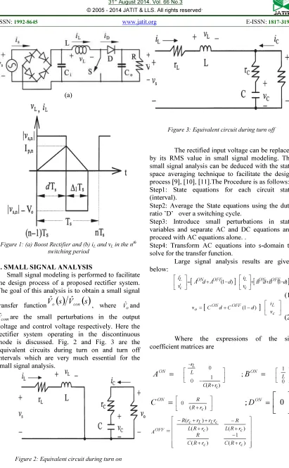
[image:2.595.92.503.84.749.2]voltage and control voltage respectively. Here the rectifier system operating in the discontinuous mode is discussed. Fig. 2 and Fig. 3 are the equivalent circuits during turn on and turn off intervals which are very much essential for the small signal analysis.
[image:2.595.91.497.98.423.2]Figure 2: Equivalent circuit during turn on
Figure 3: Equivalent circuit during turn off
The rectified input voltage can be replaced by its RMS value in small signal modeling. The small signal analysis can be deduced with the state space averaging technique to facilitate the design process [9], [10], [11].The Procedure is as follows: Step1: State equations for each circuit state (interval).
Step2: Average the State equations using the duty ratio ’D’ over a switching cycle.
Step3: Introduce small perturbations in state variables and separate AC and DC equations and proceed with AC equations alone. .
Step4: Transform AC equations into s-domain to solve for the transfer function.
Large signal analysis results are given below:
[
A d A (1 d)]
vi ON OFF
c L
− + = ′ ′
[
]
sOFF ON
c L
v d B d B v i
) 1 (− + +
(1)
[
C d C (1 d)]
vo= ON + OFF −
c L
v i
(2)
Where the expressions of the six coefficient matrices are
=
ON
A
+ − −
) (
1 0
0
c L
r R C L r
;
=
ON
B
0 1
L
=
ON
C
+
) ( 0
c r R
R
;
D
ON=
0
OFF
A =
+ − +
+ − +
+ + −
) (
1 )
(
) ( ) (
) (
c c
c c
c L L c
r R C r
R C
R
r R L
R
r R L
r r r r R
© 2005 - 2014 JATIT & LLS. All rights reserved.
ISSN: 1992-8645 www.jatit.org E-ISSN: 1817-3195
=
OFFB
cv
L
1
;
=
OFFC
+ + ) ( )( c c R rc
R r r R
R
In (1) and (2), d is the instantaneous duty cycle, which is defined as
s s ON ON s ON t T t T t t d D d ˆ ˆ ˆ + + = = +
= (3)
After the second order terms are neglected
d
ˆ
can be expressed as s s ON on s t T T t T
dˆ 1 ˆ ˆ
2 −
= (4)
In (3) and (4), lower case letters are instantaneous values, the steady state quantities are represented by the uppercase letters, and lowercase letters with caps mean small perturbations. In the boundary of DCM control, the peak value of the inductor current equals to twice the average value then L v v t t
iL (s ON)(o s)
2 = − − (5)
From the above equation after the second order
effects are neglected,
t
ˆ
ONcan then be expressed as
o s L s s s o L L s o ON v V V LI t v V V LI i V V L t ˆ ) ( 2 ˆ ˆ ) ( 2 ˆ ) ( 2 ˆ 2 2 − + + − − − − = (6)
By introducing small perturbations into (1) and
(2) and then substituting
d
ˆ
with (4) andt
ˆ
ON with (6), we can obtain
[
]
To s s C L o C L v t v v i K v v i ˆ ˆ ˆ ˆ ˆ ˆ ˆ ˆ = (7)
Where K is a 3
×
5 co-efficient matrix. Theexpressions for
k
ij are given in the Table 1. Ofwhich the matrix elements
k
ij are functions of thecircuit parameters and steady state quantities of the circuit variables. Appling Laplace transformation to both sides of equations (1) and (2) and after rearranging the equations as we obtain equation (8)
Table1 :Expressions for kij
K11 c off on L off on s s o off
on A A I A A V
T V V L D A D
A [( ) ( )
) (
2 ) 1
( 11 11 12 12
11
11 − + −
− − − + K12 ) 1 ( 12
12 D A D
A on + off −
K13 ] ) ( ) [( ) ( 2 ) 1
( 11 11 12 12
2 11 11 c off on L off on s s o L off
on A A I A A V
T V V LI D B D
B − + −
− − − + K14 ) ( 1 11 12
11onL onC off S
S V B V A I A
T + +
K15 ] ) ( ) [( ) ( 2 12 12 11 11 2 C off on L off on s s o
L A A I A A V
T V V LI − + − − K21 off s s o L off on A T V V LI D A D A 21 21
21 ( )
2 ) 1 ( − + − + K
22 (1 )
22
22 D A D
A on + off −
K 23 ] ) ( ) [( ) ( 2 ) 1
( 21 21 22 22
2 21
21 on offL on offc s
s o
L off
on A A I A A V
T V V LI D B D
B − + −
− − − + K24 ) ( 1 21 22
21on L on C off S S V B V A I A
T + +
K25 + − + − − C off on L off on s s o
L A A I A A V
T V V LI ) ( ) [( ) ( 2 22 22 21 21 2 ] ) (B21on−B21off VS
K31 ] ) ( ) [( ) ( 2 ) 1
( 11 11 12 12
11 11 c off on L off on s s o off
on C C I C C V
T V V L D C D
C − + −
− − − + K32 ) 1 ( 12
12 D C D
C on + off −
K33 ] 12 12 11 11
2 [( ) ( )
) ( 2 C off on L off on s s o
L C C I C C V
T V V LI − + − − − K34 ) ( 1
12off C O S V V C T − K 35 ] 12 12 11 11
2 [( ) ( )
) ( 2 C off on L off on s s o
L C C I C C V
T V V LI − + − − 11 15 14 13
12 ˆ( ) ˆ ( ) ˆ( ) ˆ ( )
) ( ˆ k s s V k s T k s V k s V k s
I c s s o
L − + + + = (8) 22 25 24 23
21ˆ ( ) ˆ ( ) ˆ( ) ˆ ( )
) ( ˆ k s s V k s T k s V k s I k s
V L s s o
c − + + + = (9) 35 34 33 32 31 1 ) ( ˆ ) ( ˆ ) ( ˆ ) ( ˆ ) ( ˆ k s T k s V k s V k s I k s
V L c s s
ISSN: 1992-8645 www.jatit.org E-ISSN: 1817-3195
Substituting (8) and (9) into (10) and
letting
V
ˆ
s(
s
)
=
0,a small signal transfer function relating the output voltage and the switching period are as follows0 1 2 2
0 1 2 2 0
) ( ˆ
) ( ˆ
a s a s a
b s b s b
s T
s V
s + +
+ + =
(11)
where i
a
andi
b
are the functions ofij
k
[image:4.595.84.298.105.380.2]and listed in Table 2
Table 2:
i
a
andi
b
in terms ofij
k
For a PWM controller, assuming that the
amplitude of the triangular carrier is
A
Tin voltsand the switching frequency
f
sin hertz, then the small signal transfer function from the switchingperiod to the control voltage
V
ˆ
con(
s
)
isT s
s T con
s
A T f A s V
s T
= ×
= 1
) ( ˆ
) ( ˆ
(12)
Thus, the open loop transfer function of the proposed rectifier system is
T s con
o OL
A a s a s a
T b s b s b
s V
s V s G
0 1 2 2
0 1 2 2 ) ( ˆ
) ( ˆ ) ( ˆ
+ +
+ + =
= (13)
With the above expression stability of the system can be analysed and thereby controller can be designed for the satisfactory closed loop compensation.
4. CONTROL TECHNIQUES
Two types of control techniques employed here is (Pulse Width Modulation (PWM) Technique and Variable Frequency Control Technique. In PWM Control the widths of pulses can be varied to control the output voltage. In variable frequency control the frequency is varied over wide range to obtain the full output voltage range. Figure 4shows the block diagram of the boost rectifier with control
where ABS,DIV,and VFC perform operations of absolute value, analog division and voltage to frequency conversion respectively. For an output power Po=75W the circuit is simulated in
MATLAB software with the following
specifications: Supply voltage Vs =110Vrms;
switching frequency fs= 40 KHz; Output voltage
Vo= 200 V; Load resistance R=530Ω; Inductance
L=500 µH; Input capacitance
C
i=8 µF and output capacitance Co= 2700 µF. The boost rectifieroperating in discontinuous conduction mode is
modeled and simulated using
[image:4.595.307.506.298.457.2]MATLAB/SIMULINK software.
Figure 4: Block Diagram of the Boost Rectifier with the Control
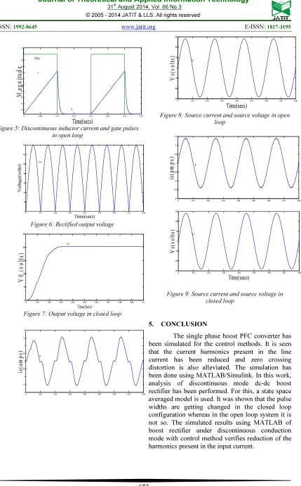
From the open loop result, we conclude that the pulse widths are constant and are shown in Fig.5and to overcome this we have to employ the control technique which eliminates this problem. Here the open loop rectifier model is operating in discontinuous mode of conduction. Input voltage 110 Vrms is applied to the rectifier and the rectified
output voltage obtained is shown in Fig.6.Here the rectifier feeds the boost converter. The output voltage during closed loop operation is shown in Fig.7.From Fig.8 we infer that the zero crossing of source current & voltage is not same. Also, source current contains harmonics. These harmonics can be reduced by employing the control techniques which are mentioned previously. It is understood that from Fig.9 the zero crossing of the two wave forms are same and harmonics is also reduced approximately around 20% and also the source current follows the sinusoidal nature of the source voltage.The THD value of source current is reduced from 30.47% to 10.45%which as per the IEEE standard there is significant reduction in harmonics. a0
) (
) (
) )(
1
(−K35K11K22−K12K21+K31K15K22−K12K25+K32K25K11−K21K15
a1
25 32 15 31 22 11
35)( )
1
( −K K +K −K K +K K
−
a2 (1 ) 35 K −
b
0 K34(K11K22−K12K21)+K31(K12K24−K14K22)+K32(K21K14−K24K11)
b1
24 32 14 31 22 11
34(K K ) K K K K
K + + +
−
b2
© 2005 - 2014 JATIT & LLS. All rights reserved.
ISSN: 1992-8645 www.jatit.org E-ISSN: 1817-3195
0 0.005 0.01 0.015 0.02 0.025 0.03 0.035 0.1
0.2 0.3 0.4 0.5 0.6 0.7 0.8 0.9 1 1.1
Time(secs)
M
a
g
n
it
u
d
e
Pulses
[image:5.595.93.522.77.768.2]iL
Figure 5: Discontinuous inductor current and gate pulses in open loop
0 0.01 0.02 0.03 0.04 0.05 0.06 0.07 0.08
0 20 40 60 80 100 120 140
Time(secs)
Vo
lt
a
g
e(
vo
lt
s)
Vrec
Figure 6: Rectified output voltage
0 0.01 0.02 0.03 0.04 0.05 0.06 0.07 0.08 0.09 0.1 0
50 100 150 200 250
Time(Secs)
V
0
(
v
o
lt
s)
V0
Figure 7: Output voltage in closed loop
0 0.01 0.02 0.03 0.04 0.05 0.06 0.07 0.08 -2
-1.5 -1 -0.5 0 0.5 1 1.5 2
is
(a
m
p
s) is
0 0.01 0.02 0.03 0.04 0.05 0.06 0.07 0.08 -150
-100 -50 0 50 100 150
V
s(
v
o
lt
s)
Time(secs)
Vs
Figure 8: Source current and source voltage in open loop
0 0.01 0.02 0.03 0.04 0.05 0.06 0.07 0.08 -0.2
-0.15 -0.1 -0.05 0 0.05 0.1 0.15
is
(a
m
p
s)
is
0 0.01 0.02 0.03 0.04 0.05 0.06 0.07 0.08
-150 -100 -50 0 50 100 150
V
s(
v
o
lt
s)
Time(secs) Vs
Figure 9: Source current and source voltage in closed loop
5. CONCLUSION
[image:5.595.332.522.267.475.2]ISSN: 1992-8645 www.jatit.org E-ISSN: 1817-3195
REFRENCES:
[1] E. J. P.Mascarenhas, “Hysteresis control of a continuous boost regulator,”in IEE Colloq. Static Power Convers., 1992, pp. 7/1–7/4. [2] C. Zhou, R. B. Ridley, and F. C. Lee, “Design
and analysis of a hysteretic boost power factor correction circuit,” in Proc. IEEE PESC, 1990,pp. 800–807.
[3] K. H. Liu and Y. L. Lin, “Current waveform distortion in power factor correction circuits
employing discontinuous-mode boost
converters,” in Proc. IEEE PESC, 1989, pp. 825–829.
[4] R. Richard, “Reducing distortion in boost rectifiers with automatic control,” in Proc. IEEE APEC, 1997, pp. 74–80.
[5] D. F. Weng and S. Yuvarajan, “Constant-switching-frequency AC–DC converter using second-harmonic-injected PWM,” IEEE Trans. Power Electron., vol. 11, no. 1, pp. 115–121, Jan. 1996.
[6] D. Simonnetti, J. Sebastian, J. A. Cobos, and J. Uceda, “Analysis of the conduction boundary of a boost PFP fed by universal input,” in
Proc.IEEE PESC, 1996, pp. 1204–1208. [7] Y. K. Lo, S. Y. Ou, andJ. Y.Lin, “Switching
frequency control for control for regulated discontinuous conduction mode boost rectifiers,” IEEE Trans.Industrial Electron Vol.54 no.2, pp 115-121Apr 2007.
[8] Y. K. Lo, S. Y. Ou, and T. H. Song, “Varying duty cycle control for discontinuous conduction mode boost rectifiers,” in Proc. IEEE PEDS, 2001, pp. 149–151.
[9] Kinattingal Sundareswaran and V. T. Sreedevi,“Boost converter controller design
using Queen-bee-assisted GA”, IEEE
Transactions on industrial electronics, vol. 56, no. 3, March 2009.
[10]G. Seshagiri Rao, S. Raghu, and N. Rajasekaran, “Design of Feedback Controller for Boost Converter Using Optimization Technique’’,International Journal of Power Electronics and Drive System(IJPEDS) Vol. 3, No. 1, pp. 117-128,March 2013.