EK-RQDX l-UG-OO 1
RQDXl
EK-RQDX
l-UG-OO
1
RQOXl
Contr()lIer Module
IUser's Guide
Prepared by Educational Services
of
First Edition" January 1984
Copyright © 1984 by Digital Equipment Corporation
All Rights Reserved
Printed in U.S.A.
The material in this document is for informational purposes and is subject to change without notice; it should not be construed as a commitment by Digital Equipment Corporation. Digital Equipment Corporation assumes no respons-ibility for any errors that may appear in this document.
Notice: This equipment generates, uses, and may emit radio frequency energy. The equipment has been type tested and found to comply with the limits for a Class A computing device pursuant to Subpart J of Part 15 of FCC Rules, which are designed to provide reasonable protection against such radio frequency interference when operated in a commercial environment. Operation ofthis equipment in a residential area may cause interference in which case the user at his own expense may be required to take measures to correct the interference.
The manuscript for this book was created using aD I G IT AL Word Processing System and, via a translation program, was automatically typeset on DIGITAL's DECset Integrated Publishing System. Book production was done by Educational Services Development and Publishing in Marlboro and Bedford, MA.
The following are trademarks of Digital Equipment Corporation.
mamaala
DEC DECnet DECUS DECsystem-l0 DECSYSTEM-20 DECwriter DIBOL DIGITAL EduSystem
lAS LA
LETTERPRINTER 100 LETTERWRITER 100 LSI-II
MASSBUS MICRO/PDP-II MINC-II OMNIBUS OS/8
PREFACE CHAPTER 1 1.1 1.2 1.3 1.3.1 1.3.2 1.3.3 1.3.4 CHAPTER 2 2.1 2.2 2.3 2.4 2.5 2.6 2.7 2.8 2.9 2.10 2.11 2.12 2.13 2.14 2.15 2.16 2.17 2.18 2.19 CHAPTER 3 3.1 3.2 3.3 3.4 3.5 3.6 3.7 3.7.1 3.7.2
CON1'ENTS
Page INTRODUCTIONDESCRIPTION ... " ... 1-1 FEATURES ... " ... 1-2 SPECIFICATIONS ... , . . . .. 1-2 RQDXl Disk Controller Module. . .. . . .. 1-2 RD51 Disk Drive ... " . . . .. 1-3 RX50 Diskette Drive ... " . . . .. . . .. . . .. 1-4 RQDXI-E Extender Module Option... . ... ... ... 1-6
FUNCTIONAL DESCRIPTION
INTRODUCTION ... " . . . .. 2-1 BLOCK DIAGRAM DESCRIPTION. . . .. 2-1 SHUFFLE STEP OSCILLATOR ... 2-3 PHASE LOCKED LOOP ... " . . . .. 2-4 DATA RECOVERY ... " ... 2-5 SYNC MARK DETECTOR ... ,. . . . .. 2-5 SERIALIZER/DESERIALIZER . . . .. 2-6 MFM ENCODER/PRECOMP GrENERATOR ... 2-6 INTERRUPT VECTOR REGISTER. . . .. 2-8 SA READ REGISTER, SA WRITE REGISTER, IP REGISTER. . . .. 2-8 QBUS TRANSCEIVERS AND HANDSHAKE CONTROLLERS. . . .. 2-8 RQDXl CONTROL LOGIC ... 2-10 MEMORY ADDRESS COUNTER/REGISTER ... 2-12
2 K X 16 RAM ... 2-12
DISK DRIVE CONTROL REGISTER AND STATUS BUFFER ... 2-12 T-l1 RAM ADDRESS POINTER AND ALU ... 2-14 BIDIRECTIONAL BYTE MULTIPLEXER ... 2-14
8 K X 16 PROM ... 2-14
QBUS DMA POINTER AND ALU ... 2-14
CONFIGURATION AND INSTALLATION
CHAPTER 4
4.1 4.2 4.2.1 4.2.2 4.3 4.3.1 4.3.2 4.4 4.4.1 4.4.2
CHAPTERS
5.1
5.2 5.3
CHAPTER 6
6.1 6.2 6.2.1 6.2.2 6.3
CONTENTS (Cont)
Page
REGISTERS AND COMMANDS
INTRODUCTION. . . .. 4-1 REGISTERS ... 4-1 Initialize and Poll Register (IP). . . .. 4-1 Status and Address Register (SA) ... ' . . . .. 4-1 MASS STORAGE CONTROL PROTOCOL (MSCP) ... " . . . .. 4-2 MSCP Commands ... " . . . .. 4-3 MSCP Status Codes ... " .. '. . . .. 4-4 DIAGNOSTICS AND UTILITIES PROTOCOL (DUP) ... " . . . .. 4-5 DUP Commands ... " ... 4-5 DUP Responses ... " ... 4-6
ERROR DETECTION
INTRODUCTION ... " ... '. . . . .. 5-1 DIAGNOSTIC LED ERROR DISPLAYS ... '. . . . .. 5-1 DIAGNOSTIC SOFTWARE ... '. . . . .. 5-3
DISK DRIVES
INTRODUCTION. . . .. 6-1 RD51 DISK DRIVE ... 6-1 RD51 Disk Drive Installation. . . .. 6-2 Formatting the RD51 Disk Drive. . . .. 6-3 RX50 DISKETTE DRIVE. . . .. 6-4
APPENDIX A RQDXl CONTROLLER MODULE BACKPLANE PIN ASSIGNM:ENTS
APPENDIX B RQDXl CONTROLLER MODULE CABLE SIGNALS
APPENDIX C DISK DRIVE CABLE CONNECTOR PIN ASSIGNMENTS
C.1 C.2
RD51 DISK DRIVE CONNECTOR PIN ASSIGNMENTS. . . .. C-l RX50 DISKETTE DRIVE CONNECTOR PIN ASSIGNMENTS .... ' . . . .. C-3
Figure No. 2-1 2-2 2-3 2-4 2-5 2-6 2-7 2-8 2-9 3-1 3-2 3-3 3-4 3-5 3-6 4-1 5-1 6-1 6-2 6-3 6-4 6-5 A-I Table No. 1-1 3-1 3-2 3-3 4-1 4-2 4-3 5-1 5-2 6-1 A-I B-1 C-l C-2 C-3 C-4 C-5
FIG1JRES
Title Page
RQDXl Controller Module Functional Block Diagram ... 2-2 Shuffle Step Oscillator . . . .. 2-3 Phase Locked Loop Logic ... 2-4 Data Recovery and Sync Mark D(:tector Logic. . . .. 2-5 Serializer/Deserializer and MFM Encoder/Precomp Generator Logic . . . .. 2-7 Interrupt Vector Register, SA Regiisters and QBus Interface Logic. . . . .. 2-9 T-ll, RAM and ROM Logic ... 2-10 Main High-Speed Controller Architecture ... 2-11 Disk Drive Control Register and Status Buffer ... 2-13 RQDXl Controller Module Jumpier and LED Locations ... 3-1 RQDXl Address Selection Jump(~r Format .. . . ... . . .. . . .. 3-2 RQDXl Logical Unit Number Jumper Format . . . .. 3-3 RQDXl MICRO/PDP-II Signal Distribution Connections. . . .. 3-4 RQDXI-E Extender Module Jumper Locations ... 3-5 RQDXI-E Extender Module Connections ... 3-6 Memory "Communications Area" Organization. . . .. 4-2 Diagnostic LED Locations. . . .. 5-1 RD51 Disk Drive. . . .. 6-1 RD51 Disk Drive Read/Write Printed Circuit Board. . . .. 6-2 RD51 Disk Drive Head Positioner Flag ... 6-3 RD51 Serial "Number Label Location. . . .. 6-4 RX50 Diskette Drive . . . .. 6-5 Quad Module Contact Finger Identification ... A-I
TAB:LES
Title Page
PREFACE
This user's guide provides information on the configuration, installation, and operation of the RQDX I disk drive controller module, the associated disks (the RD51 Winchester fixed disk drive and the RX50 diskette drive), and the RQDXI-E extender module option.
Chapter I provides environmental and functional specifications for the RQDXI controller module, the RD51 fixed disk drive, the RX50 diskette drive, and the RQDX I-E extender module option.
Chapter 2 gives a functional description of the RQDX I controller module.
Chapter 3 presents configuration and installation information for the RQDX I controller module and the RQDX I-E extender module option.
Chapter 4 describes the programmable registers that are LSI-II bus addressable on the RQDX I controller module. Mass storage control protocol (MSCP) and diagnostics and utilities protocol (DUP) are also briefly described.
Chapter 5 provides testing and error detection information.
Chapter 6 presents installation and operation information for the RD51 fixed disk drive and the RX50 diskette drive.
RELATED DOCUMENTATION
The following documents provide additional information and may be of interest to RQDXI controller module users.
Document Title
RQDX I Field Maintenance Print Set UDA50 Programmer's Documentation Kit
Document Number
MP-OI731-01 QP-905-GZ
In addition, users may refer to documentation for the specific system in which the RQDXI controller
1.1 DESCRIPTION
CHAPTER 1
INTRODUCTION
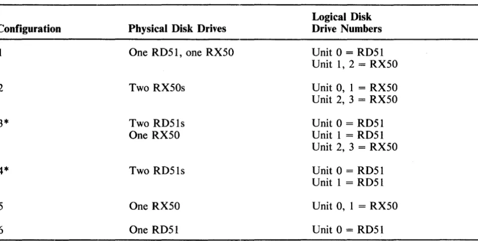
The RQDX 1 disk drive controller module interfaces, the RD5I disk and/or RX50 diskette drives to any quad- or hex-size backplane that uses a 16-, 18-, or 22-bit LSI-II bus. The backplane must be in a mounting box (such as a BA23) that provides a control panel and a signal distribution panel. A single RQDX 1 module controls anyone of the configurations listed in Table 1-1.
Configuration
2
3*
4*
5
6
Table 1-1 RQDXl Controller Module Configurations
Physical Disk Drives
One RD51, one RX50
Two RX50s
Two RD51s One RX50
Two RD51s
One RX50
One RD51
Logical Disk Drive Numbers
Unit 0 = RD51 Unit 1, 2
=
RX50 Unit 0, 1 = RX50Unit 2, 3
=
RX50 Unit 0 = RD51 Unit 1=
RD51 Unit 2, 3 = RX50Unit 0 = RD51 Unit 1 = RD51
Unit 0, 1 = RX50
Unit 0
=
RD51*
These configurations require the use of the optional RQDX J-E extender module. Refer to Paragraph 3.7 for additional RQDX J-E information.The RD51 disk drive is a random access storage device, which uses two non removable 133.4 mm (5.25 inch) disks as storage media. The RD51 disk drive has a total formatted storage capacity of II megabytes.
The RX50 diskette drive is a random access storage device, which uses two single-sided 133.4 mm (5.25 inch) RX50K diskettes. The total storage capacity of the RX50 diskette drive is 800 kilobytes of formatted data.
[image:10.615.69.546.309.549.2]1.2 FEATURES
The RQDX I controller module has the following features.
• Single quad-size module.
• Supports DMA data transfers in 16-, 18-, or 22-bit addressing modes.
• Supports block mode transfers with MSVII-P memories.
• Supports 22-bit addressing on an LSI-II bus.
• Memory parity error abort feature for use with memories that have a parity option.
• Requires no jumper/switch reconfiguration when adding or removing RDSI or RXSO drives.
1.3 SPECIFICATIONS
1.3.1 RQDXl Disk Controller Module
Module
Size
Power Requirements
Bus Loads
AC Bus Loads DC Bus Loads
Addressing Modes
Limitations
Drives Per Controller
LSI-II Bus-Addressable Registers
Base Device Address (Standard)
I quad-size module, M8639
Height: 26.S6 cm (10.46 in) Width: 1.27 cm (O.S in) Length: 22.70 cm (8.94 in)
+S Vdc ±S% at 6.4 A (typical) 8.0 A (maximum)
+12 Vdc ±S% at 7.3 rnA (typical) 10 rnA (maximum)
2.S
I
16-, 18-, and 22-bit (determined by user)
The RQDX I will not fit in the dual-height LSI-II mini-series H9281 backplane.
Up to four logical units, no more than two RDSI disk drives
2
Addressing Mode
16-bit 18-bit 22-bit
1-2
Address (Octal)
1721S0 7721S0
Vector
Data Transfer Rate
Environmental Specifications
Temperature
Storage Operating
Relative Humidity
Storage Operating
Altitude
Storage Operating
Airflow
Operating up to 50°C
t .3.2 RD5
t
Disk DriveStorage Type
Medium
Recording Surfaces
Magnetic Heads
Recording Method
Performance Specifications
Recording Capacity (Formatted)
Bytes Per Sector
Sectors Per Track
Tracks Per Group
Software selectable (I\rormally set at 154)
800 ns/word (peak) controller to host
-40°C to 66°C (-40°F to 150°F) 5°C to 50°C (41°F to 122°F)
10% to 95%, noncondensing 10% to 95%, non condensing
9.1 km (30,000 ft) maximum 2.4 km (8,000 ft) maximum
Maximum temperature rise across module must not exceed 20°C (68°F) input to output.
Winchester fixed disk
4 data surfaces
4 read/write heads
Modified frequency modulation (MFM)
512 bytes
18 sectors (track size)
Each sector has a logical block number (LBN)
Groups Per Cylinder
Cylinders Per Unit
Total Cylinders Per Unit
Total Bytes Per U ni t
Transfer Rate
3 groups (cylinder size)
100 cylinders
102 cylinders
*
11.059 M bytes
5,000,000 bits/s (625 K bytes/s)
Access Time (Buffered Seek, Including Settling)
Average
Maximum
A verage Latency
Functional Specifications
Rotational Speed
Recording Density
Track Density
Environmental Specifications
Ambient Temperature
Relative Humidity
Maximum Wet Bulb
1.3.3 RXSO Diskette Drive
Storage Type
Medium
Recording Surfaces
Magnetic Heads
Recording Method
*
Cylinders 100 and 101 are assigned as follows. Cylinder 100, Group 0:Cylinder 100, Groups I, 2: Cylinder 101, Groups 0, I: Cylinder 101, Group 2:
85 ms
205 ms
8.33 ms
3,600 r/min (±1 %)
9,074 bits/in (maximum)
345 tracks/in
20% to 80% noncondensing
Diskette
2 data surfaces
2 read/write heads
Modified frequency modulation (MFM)
Replacement and caching table (RCT) Format control table (FCT)
Replacement block numbers (RBNs) Diagnostic block numbers (DBNs) Reserved
Performance Specifications
Recording Capacity (Formatted)
Bytes Per Sector
Sectors Per Track
Tracks Per Group
Groups Per Cylinder
Cylinders Per Surface
Bytes Per Surface
Surfaces Per Unit
Bytes Per Unit
Transfer Rate
Access Time
Track to Track
Head Settling Time
Head Load Time
Rotational Latency
Random Access
Drive Motor Start
Functional Specifications
Rotational Speed
Recording Density
Track Density
Environmental Specifications
Ambient Temperature
Relative Humidity
Maximum Wet Bulb
512 bytes
10 sectors (track size)
Each sector has a logical block number (LBN).
5 tracks (group size)
16 groups (cylinder size)
1 cylinder
404,480 bytes
2 surfaces (2 diskettes)
808,960 bytes
250,000 bits/s (31.25 K bytes/s)
Minimum
6 ms
Typical
100 ms
264 ms
300 r/min (±1.5%)
5,576 bits/in (maximum)
96 tracks/in
20% to 80% non condensing
Maximum
30 ms
30 ms
200 ms
1.3.4 RQDXI-E Extender Module Option
Module
Size
Power Requirements
Bus Loads
AC Bus Loads DC Bus Loads
Limitations
Environmental Specifications
Temperature
Storage Operating
Relative Humidity
Storage Operating
Altitude
Storage Operating
Airflow
Operating up to SO°C
1 dual-size module, M7 S12
Height: 13.2 cm (S.2 in) Width: 1.27 cm (O.S in) Length: 22.8 cm (8.9 in)
+S Vdc at O.S A (typical)
o
o
0.6 A (maximum)
Provides signal distribution to a single disk or diskette drive
Cannot be used on the PDP-II /23 Plus
-40°C to 66°C (-40°F to IS0°F) SoC to 60°C (41°F to 140°F)
10% to 9S%, noncondensing 10% to 9S%, noncondensing
9.1 km (30,000 ft) maximum 2.4 km (8,000 ft) maximum
Maximum temperature rise across module must not exceed 20°C (68°F) input to output.
2.1 INTRODUCTION
CHAPTER 2
FUNCTIONAL DESCRIPTION
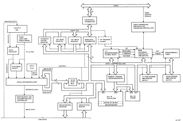
The RQDX I controller module interfaces the RD51 disk drive and/or RX50 diskette drives to a 16-, 18-, or 22-bit LSI-II bus. One RQDXI controller module can support up to four logical units in any combination of RD51 and RX50 drives (up to two RD51 drives per RQDX I controller module). The RQDX I controller module (M8639) has the LSI-II bus transceivers and decoders, programmable regis-ters, controller timing and sequence logic, and the data formatting circuits necessary to read and write on lthe RD51 disk media and/or the RX50 diskette media.
:!.2 BLOCK DIAGRAM DESCRIPTION
The main functional subsections of the RQDX I module are shown on the block diagram in Figure 2-1. The block diagram illustrates the basic architecture and the data path relationships of the major subsec-tions. The RQDX I controller module is a bus-oriented system controlled by a system control function shared by the T-II chip and the main high-speed controller.
The major subsections of the RQDX I are as follows.
• Shuffle step oscillator • Phase locked loop • Data recovery • Sync mark detector • Serializer / deserializer
• MFM encoder /precomp generator • Interrupt vector register
• SA read/write registers, IP register
• QBus transceivers and handshake controlle:r
• RQDX 1 control logic: T-II chip and main high-speed controller • Memory address counter/register
• 2 K X 16 RAM
• Disk drive control register and status buffer
• T -I I RAM address pointer and arithmetic logic unit (ALU) • Bidirectional byte multiplexer
• 8 K X 16 PROM
tv
I
tv
SE R IALIZE R/DESER IALIZER
NRZWRITE DATA
MFM ENCODER AND PRECOMPENSATION CONTROLLER
WRITE DATA
DISK DRIVE
.. CONTROL ..
Cl-BUS
GO
Q-BUS CONTROL SIGNALS
Q-BUS TRANSCEIVER AND SATELLITE HANDSHAKE CONTROLLERS
T11 REQTlIDMA MAIN
HIGH SPEED CONTROLLER (100 nslSTATE) MICROPROCESSOR Tll DMAACK
(7_5 MHZ, 16 BIT) 1 - - - . 1
2K x 16 STATIC RAM DEVICE CTl BLOCK
-SECTOR BUFFER
TAKE BUS
8K x 16 EPROM
Figure 2-1 RQDX 1 Controller Module Functional Block Diagram
INIT
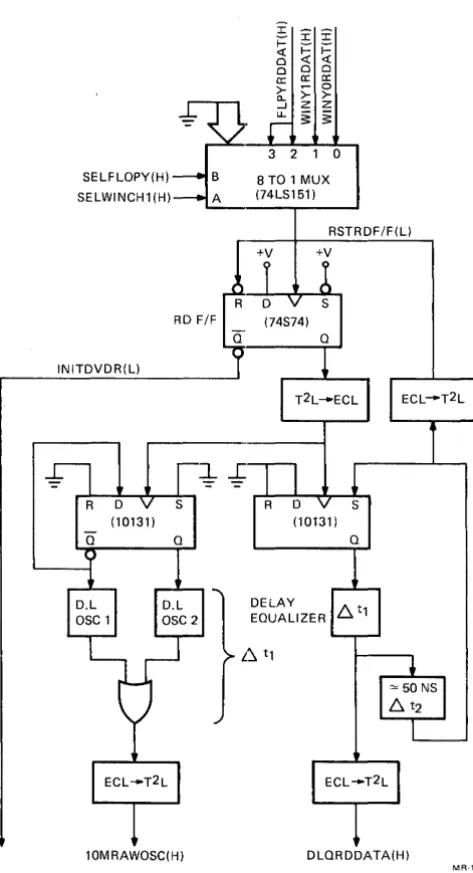
[image:17.792.103.716.83.491.2]2.3 SHUFFLE STEP OSCILLATOR
The shuffle step oscillator (Figure 2-2) is a system of two matched 10 MHz oscillators, a small asynchro-nous oscillator controller, and a read data delay equalizer. When one of the oscillators is generating a raw read clock signal for the phase locked loop (PLL), the other oscillator is in stand-by. At each raw read data pulse, the active oscillator is commanded to turn off and the stand-by oscillator is commanded to become active. This causes the oscillators to "shuffle" to keep in step with the RAW read data. The read data delay equalizer section delays the RAW read data to compensate for the short amount of time that it takes to shuffle the oscillators.
£
'
3 2 1 0SELFLOPY(H) B 8 TO 1 MUX SELWINCH1(H) A (74LS151)
RSTRDF/F(L)
RD F/F
INITDVDR(L)
10MRAWOSC(H) DLQRDDATA(H)
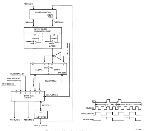
[image:18.615.185.422.185.622.2]2.4 PHASE LOCKED LOOP
The phase locked loop (PLL) logic is shown in Figure 2-3. The PLL is a dual-channel, single··mode system. Dual channel provides one channel for the RX50 diskette drive(s} and one channel for the RD51 disk drive(s}. The function of the PLL logic is to provide the "flywheel" effect for the shuffle step oscillator output, thus integrating the effects of the "pulse drift" in the RAW read data. The output of the PLL is fed into a counter which generates two data recovery window signals. These "windows" are generated in a way to center the read data pulses. (At any given time the data will be framed by one of these windows.) The proper data framing window is selected automatically by the sync mark detector.
DLQRDDATA(H)
10MRAW05C(H)
500KHZ05C(H)
!
1 0
REFCLK(H)
PHASE DETECTOR
(74574 74564)
~ ")
PMPUP(L) PMPDWN(L)
. . ~
ACTIVE FILTER AND CHARGE PUMP
o
~~arjE;r
: (LF347)
~
1 0
VC E I VC
I
DUAL VCO
!
EFLOPPY : WINNY
I (74L5626)
() :i (5
u
> 20MHZVCO(L)
N
:c
~
() ()
1 0
2TO 1 MUX 5 5ELFLOPY(H)
(745157)
C)
2XVCO(L)
()
REFCLK(H) RDDATA(H)
VCOOUTPUT(H) x >= CI.. o ..J U. ..J W V)
~
BITCELL ~2XVCO(H)
VCOOUTPUT(~~
AWINDOW('L-J
MR-'1290 Figure 2-3 Phase Locked Loop Logic
[image:19.613.70.566.180.630.2]2.5 DATA RECOVERY
The data recovery logic (Figure 2-4) consists of two single-bit, edge-triggered, double-buffered registers. The registers are cross-coupled in order to capture the read data occurring anywhere within either data framing window. Together with the phase locked loop output, an NRZ read data stream is produced.
2.6 SYNC MARK DETECTOR
The sync mark detector logic (Figure 2-4) provides two functions. One, it detects the sync mark, and, two, it selects the proper stream from the data recovery logic. Both data recovery bit streams are analyzed to find the sync mark. Upon detection of the sync mark in either stream, the serializer/deserializer logic receives the desired data stream.
SERLSRCLK(H)
SERLSRCLK
"vca OUTPUT"
AWINDOW
ADRMRKFND(H)
VCOOUTPUT(H)
--,
c~~~
!
I
STATE REGISTEF]
I
.J.A~~S~
OJ
Z
:0
N
o
»
--I
:c
»
z
:0
N
o
»
--I
~
MFM _ _ +-' '--~"-T--+~ 'T~-~ ' - -__ .I.1If:_---'n
BNRZDAT
I nl...-+-_ _ } WHEN WINDOW
o ~O 0 IS LOCKED TO
-. _:-+--....J 1 Al CELL BOUNDRYS
[image:20.615.120.508.197.698.2]"CLOCKS"
... --"--~---L-'f-"---' ;-~., 0 OA
AN RZDAT _ _ _ - '
MFM n n
n
I I ___ JI I i
'---+---ANRZDAT~_~~~
BNRZDAT
~~1-'
0 I~~
ADF:MRKFND(H)
r
-}
WHEN WINDOW IS LOCKED TO CELL CENTERS "ONES"
MR-11288
2.7 SERIALIZER/DESERIALIZER
The serializer /deserializer is shown in Figure 2-5 and consists of the following four parts.
• A double-buffered serial in/parallel out register • A double-buffered parallel in/serial out register • A
eRe
generator/checker• A high-speed finite state machine controller
The serial in/parallel out (SIPO) logic shifts the serial read data through the
eRe
generator and forms an 8-bit parallel byte. The byte is buffered for data transfer.The parallel in/serial out (PISO) logic receives the parallel write data, buffers it, and shifts this data serially through the
eRe
generator to the MFM encoder and precomp generator. This serial data becomes the write data to be sent to the disk.Both the SIPO and the PISO logic are controlled by the high-speed machine controller.
2.8 MFM ENCODER/PRECOMP GENERATOR
The MFM encoder /precomp generator logic (Figure 2-5) receives the serial data to be written to the disk and performs the following operations.
1. It generates a modified frequency modulation (MFM) data bit stream.
2. It precompensates the MFM bit stream (for both the RD51 disk drive and the RX50 diskette drive).
3. It generates the sync mark bit sequence on command.
N
I
-J
r
( ~
W/RBUFFLG (H)l ~ : 2
-~ J: - J: ...J 0
-'" a:
t-~ t- ~
2 ~
...J 0 w
t-~
t-U oc
~
;:~ 8
NRZRDATA (H) a:
ADRMRKFND (H)
r---~t-t--I
~H~ ~
&l
W/R BUF FLG
I
t- ;: a: '" U(74LS74) ~ ~ o « J: a:
U U
R :1 g O d d
1
a: a: a:L
LJ,eUAL RANK BYTEJ
-=t::.
CTRL HOLD REGr---I~r> (2 x 74LS175) LASTWORD (H) ~ LOADREGS (H) SLOADPISO (L) SHIFTREGS (H)
2
~
en
~
HIGH SPEED CONTROLLER
A
<'r-.
'I1B
L..-_ _ _ _ _ - ,
J SER SIPO
I
rt
SCLK (74LSl64)~~
' -~ OE B BIT REGISTERI
r -~ LD (74LS374)
I
I IL..---'
DAL(7:Q) (H)
J
-I
HOLDING REGISTERL
(74LS374)J
NRZDOUT (H)
LDPISOBUF (H)
1
c","'o",":
I
ERROR FLGI
(74LS74)D
ERR
CRCDOUT (H) PRESETCRC (L) ~
:1rJ
rt
: I
"XT"""OG"
I:
L -________________________ ~---~S~E~L~CH~K~W~R~D~(~L~)---~-tsc~C~UXJ
UPSTRMNRZ (H) I
I ~ I
r=~'~'"'j-
+
~ATf::'"
I!
REQADRMRK (H)r
I
I
I
I,
I
o 0 d 0
r---~~~~~~--«
m~+-;;t--:I~AL
TIME I SELPRECOMP1 (H) } T11L (PALl6R4).
L---,-. -
V -
~I
OUTPUT DECODER 1(PALl6L8)I ENBLBNDRY (L) ENBLCENTR (L) SHIFTREGS (H)
r---~r_ r-____ + - . _ _ _ _ _ _ _ _ _ _ ~S~E~LP~R~E~C~OM~P~O~(~H)~_
I I
1
I SELFLOPPY (H).---~---+--'~~~A~~~--~~
j~-I---~~==~~-I BIT COUNTER
I
I
I
.1
I
IIj-t-t---t--~V I (74LS161)
I
MFM LOGIC I PRECOMP LOGIC I BITCNTR=8 (H)V
J L+1
L _ (PALl6R4.!.J MFMwRTTH)- I- -
-MISSING BIT
I
4
DECODER
I
? WRTADRMRK (L)
LAT~7:S175)
1
I
PRECOMP TIMING CONTROLLER J JPRECOMP MUX (74S151)
I
WRTDATA (H)I
I
[image:22.793.101.714.67.499.2]2.9 INTERRUPT VECTOR REGISTER
During an interrupt sequence, the contents of the interrupt vector register (Figure 2-6) are: gated to the QBus to be used as the vector. The MSCP initialization function supplies the T-ll chip on the RQDXI controller module with the vector number. The T-Il chip loads this number into the interrupt vector register.
2.10 SA READ REGISTER, SA WRITE REGISTER, IP REGISTER
The status and address registers (SA) shown in Figure 2-6 are used by the T-ll chip and the QBus processor for the MSCP port initialization sequence. Both SA registers occupy the same QBus I/O page address.
The SA read register is written into by the T-II chip and read from by the host QBus processor. This register is used to pass initialization status to the QBus processor.
The SA write register is written into by the QBus processor and read from by the T-ll chip. This register is used during the initial sequence to pass the MSCP command buffer address and interrupt vector to the T-ll chip.
The IP register is used to begin the initialization sequence when this register is written into by the QBus processor. When the host QBus processor reads from the IP register, the RQDXl controller module initiates a polling routine.
2.11 QBUS TRANSCEIVERS AND HANDSHAKE CONTROLLERS
The RQDXI controller module interfaces to the QBus through QBus drivers, QBus receivers, and control circuits. The control circuits, shown in Figure 2-6, provide the handshake signals necessary to interrupt the QBus, obtain control of the QBus for DMA, and interface the programmed SA and IP n~gisters to the QBus.
N
I
\0
I
::::;
XQDAL<l5:00>(H) ~
:;:
~
0
;;:
'ty'
~SA WRITE REG (2 x 74LS374)
TO Q BUS TRANCEIVER
::::; ;;: o f-~ > I
~ E
f- :::;
:;: <{
f- 0 f- a x
• •
::::; ~~ QBUS~'"
i ,
QBUS TRANSCEIVER,
(3 x xDS8641)
() () f) ) () () ( () () ) (
LJ'---r--T--r-r~~...-r-Tl ~~~----r--r-'
it
16}~16
I ISA READ REG VECTOR REG z z §" ~ I=" ~a:~ ~ ~ ~ ~ ~
I
"
~V
II
I I
D
~'----II--+--r-D ~---+---i~
E I I I ::::;
I
g
~
g
~ ~
!
~
(2 x 74LS374) / \ (2 x 74LS374) (1/274LS74) (1/2 74LS74) ~ ~ ~ ~ ~ f- f- f- ~~~'b~T.
~---,i'r,----,--~---"'--{I---,...;--'
::::; ADDRESS I~ HOLD
~
I
~ ~
n
~
I, LUN BUFFER , ~ I!:i
(l4LS240)
~ ::::;
II
<{ ~"-'\ 0 0 ;;:
V 15
ENBLLUN(L)
"
70
::::; ::::; ;;:
~ 0
f-Q ~
Q.
9 > 9 I
~ f-~
f-I
() II
A PIOCONTROL (PALl6LS) ::::; ::::; ::::; ::::;~ ~ ~ ~ I I
~ ;;; :;:
~
i
0 ~ 0 0 >
;;: 0 ;;: ;;: x ;;:
~
\
.
,TO T11 INTERRUPT
Tll MEMORY MAP HIGH SPEED CONTROLLER
Figure 2-6 Interrupt Vector Register, SA Registers and QBus Interface Logic
I I i I
I I I I I I
r::::i:L Z 1="(3):
~ ~ ::> z -' 0 o >- Q.
~ a: f- o '" f- f- a: a:
~ () ()
QBUS DMA REQUEST' ,'NTERRUPT , CONTROLLER CONTROLLER
(PAL 16LS) (DCOO3 1/2 74S74)
q REQVECTOR(H) I q c
§ :J
~ ~
+ a
~ ~
~
[image:24.795.100.724.139.425.2]2.12 RQDXI CONTROL LOGIC
The supervisory control of the complete RQDXl controller module is a shared function between the T-ll chip and the main high-speed controller. These two devices share the internal data address blllS (DAL bus). (Refer to Figure 2-1)
The T -11 chip has control over all housekeeping functions that are considered to be slow or those that
require data processing. The T-ll chip is configured into the 16-bit static mode driven by a 7.5 MHz
clock. The T -11 logic, along with the RAM and ROM memories, is shown in Figure 2-7.
1
7.5 MHZ XTAL OSC
HIGH SPEED \ CONT~OLLER j
:J
l. 5
...--_~ll_.w..---. al
J
S lMUX 0I
~ (74LS15S)
HIGH SPEED CONTROLLER
r
. - -_ _ _ _ _ REQTIIDMA(H) ---1
TIIDMAACK(L)
200000
117400 256 CSR'.
T·ll MEMORY MAP
1
NOT USED
INTERRUPT REGISTER PWR UP AND DMA LDGIC
NOT USED
(2 X PAL 16LS)
ASYNHOLD
+
(74LS373)
I
J
MODE BUFFER~ (1/2 74LS240)
L..-_"'--~"'--_~ /
i
4\ V :;
;3
"
"--..;
RAS(H)l ADDRESS LATCH
I
1 \
(4 X 74LS163)n
1~...--
__ -.,.. _____
-=M::EM:::A:"::;DR< ... 15_:00_>H _ _ _ _ _ ---'~~
,...---.:Io£....~---.
I
MEMORY DECODEI
rl
2K X 1~ RAMI
~~RXO::I
(74LSJO, PAL lSLS 2 x 74LS13S) ...,""""r-~~""--I~_(2_X~4~01 ... 6)....J (2 X 27M)1.U)
~~ _ _ _ ~~ _ _ _ _ ~_~~_--J ~_~~ _ _ _ ~
\
[ \ 21
W
:JW 16 f' "l' DEVICE SELECT
:J 0 :::;;
i ~
~ g
a:i a:i
Figure 2-7 T -11, RAM and ROM Logic
[image:25.617.86.549.196.598.2]The main high-speed controller controls the high-speed read, write, and DMA functions to or from host memory. This controller is configured as a microprogrammed multibranch controller operating at 10 MHz. The main high-speed controller architecture is shown in Figure 2-8.
CONTRCLK(H)
MUX1<C:A>(H)
EN4WAY(L)
NXTSTATE<9:2>(H)
r
I
I
I
CONTROL INPUTS
~
21
LDCOFLAG(H)
GO(HI
FLAGO(H)
CONTROL T11 BUS OUTPUTS OUTPUTS
(1/274LS74)
CLR WATCH DOG
TIMER (74LS292)
~
z
~
E
Cl a::« ...J
UJ U
Cl co
RESETCTL(L)
Figure 2-8 Main High-Speed Controller Architecture
7.5 MHZ
[image:26.615.66.534.129.597.2]The 1'-11 chip sets up all disk drive control signals, initializes the timer, clears the parity error flag, and resets the shuffle step oscillator. The 1'-11 chip then sets up the device control block (DCB) with parameters for the high-speed controller, initializes the response word with Is, and then sets the GO flag in the I/O map. The high-speed controller, upon receipt of the GO signal, requests direct me:mory access to the DAL bus from the T-ll chip. Upon receipt of the TI1DMAACK signal, the controll(~r takes control of the DAL bus and begins the operation specified in the function code. Upon completion, various parameters are placed in T-l1 RAM, the controller response word is filled in (in the DCB), the GO bit is cleared, and control is returned to the T -11 chip. All high-speed controller operations must be completed within 1 second or the timer logic will terminate controller operation.
2.13 MEMORY ADDRESS COUNTER/REGISTER
The memory address counter/register (shown in Figure 2-7) is used to latch the T-ll luemoryaddress during the address phase of the bus cycle. The counter function of the address register is used by the high-speed controller to form a RAM pointer which can be incremented.
2.14 2 K X 16 RAM
As shown in Figure 2-7, the 2 K X 16 RAM is divided into the following three major sections.
• 1'-11 work space • Device control block • Sector buffer
This RAM can be accessed by both the 1'-11 chip and the high-speed controller.
2.15 DISK DRIVE CONTROL REGISTER AND STATUS BUFFER
The disk drive control register and status buffer are shown in Figure 2-9. Under T -11 control, the disk drive control register provides drive selection and head control, including cylinder seeks on the selected drive. This register also contains static control information for the PLL and serializer. The drive status buffer is designed to interface the selected drive status to the DAL bus so that it can be interrogated by either the 1'-11 chip or the high-speed controller.
.." fiQ' c:: @ N I \0 0 r;;' ~ 0 :J. <: (p (j 0
=
g;....
:e""1 2- ~ 0 ~ ~ (p ~
0.9. tI:l ~
....
(")(p
~
""1
~
=
0.rJ).
....
~....
c:: tI:l t:::C c:: ~ (p ""1..
..
.. ..
.. ..
...
...
...
-...
....
....
....
....
....
£l-ZINDEX(L)
}~
-TIMEUP(HI
Lr-INDEX(L)
""'
TRACKOO(L) ..r
"'"
ENDRVSTAT(L) WRTFAULT(L) .r I'"READY(L) ..r ~
SEEKCPLT(L) ...., ~
~
DRVSL1ACK(L) .r
~ r----"1
~
DRVSLOACK(L) , ; Vi
:IJ
...aC. ~~ m
»
---.c " 0 0
"" ~ ~
r-r..c
~
~' - - - - ~
~
r
-RDl RDY(L)
f ' l
RDORDY(L)
..("1
RD1WRTPRO(L) BCLR(L)
-"
P--RDOWRTPRO(L) ,..
< - LDDRVSEL(L)
RX3WPTLED(L) ; .
0
RX2WPTLED(L) :IJ
~ RX1WPTLED(L)
(/)
RXOWPTLED(L) -1" m
r-~
m
(")
~o;
SELFLOPY(H) ;::; -ii'\.r-"" :IJ
~ m
0 »
.a> Gl
< - i SELWINCHl (H)
~
~
~»
-<
RXMOTORON(L) ~ DRVSEL4(L) ~
~
DRVSEL3(L)
*
DRVSEL2(L) DRVSEL 1(L) ~'
r
-}-
SELPRECM1(H)P-- BCLR(L)
~<
LDDRVCTRL(L)SELPRECMO(H) ~
(") REDUCWRTI(L) l ' 0
DI RECTION(L) STEP(L) HEADSEL2(L) HEADSEL1(L) -HEADSELO(L)
-~ -~
r- :IJ
[J) 0
!::l
r-W :IJ
~ ~ ." u;
~ ~
~
~
(")
o
.... WRTGATE(L)
0<::]-
WRTGAfE(H) ~:IJ
... RXWRTDATAlL) 0<
MFMWRTDT1(L) MFMWRTDTl (H)
~I
MFMWRTDTO(L) WRTDATA(H)
...
MFMWRTDTO(H)
...
m
MFMRDDATl(L) WINY1RDAT(H)
-MFMRDDATl (H)
J>
.,""'0,"'",f
~
MFMRDDATO(L) MFMRDDATO(H)
-~
-(")
~
~
-<
READDATA(L)
.{>
FLPYRDDA1(H)-I
DIAGMODE(H)
~
.-.'-J
,.~.-..'.:::.,1
,. .JS:::J..
0
:; .:'.:::.,1 Gl
Z ,.~
~III ~\:..:/
(")
r-m
0
ul
r
-0 :; ~ 0 (/) -i n :IJ m
_ Gl
" <"
""
~
~ ,-
K=--BCLR(L) LDSYSD ISP( L)2.16 T-ll RAM ADDRESS POINTER AND ALU
The T -II RAM pointer logic consists of an address counter and an ALU. The high-speed controller logic loads the beginning and ending T-ll RAM addresses into the registers within the address counter. The controller then uses these pointers to specify the locations in the T -11 RAM where data is to be transferred during QBus DMA and disk data transfers. The high-speed controller increments the pointers and monitors the ALU to determine when the ending address has been reached.
2.17 BIDIRECTIONAL BYTE MULTIPLEXER
The bidirectional byte multiplexer is used to interface the 8-bit input/output of the serializer/deserializer to the 16-bit RAM via the DAL bus.
During t~ read operation, the byte multiplexer causes the 8-bit byte from the serializer/deserializer to appear on both high and low bytes of the 16-bit DAL bus. The high-speed controller can then selectively write the byte into either the high or low byte section of the 2 K X 16 RAM.
During a write operation, the bidirectional byte multiplexer, again under control of the high-speed controller, can be used to place the high byte into the low byte position of the DAL bus. The low byte output of the RAM is disabled at this time.
2.18 8 K X 16 PROM
The 8 K X 16 PROM is used solely to store the T -11 instructions.
2.19 QBUS DMA POINTER AND ALU
The QBus DMA pointer logic consists of an address counter and an ALU. This logic is controlled by the high-speed controller and is used to hold the QBus address during a DMA process.
This logic is also used as a byte comparator. The high-speed controller utilizes this compare function to perform sector seek functions during read/write operations.
3.1 INTRODUCTION
CHAPTER 3
C01'lFIGURATION AND INSTALLATION
The RQDX 1 controller module must be mounted in the last occupied slot of the backplane due to the DMA and interrupt structure of the LSI-II bus. The module's device address and logical unit number may be changed by reconfiguring jumpers on the module. Figure 3-1 shows the RQDX 1 controller module jumper and diagnostic LED locations.
07 08 D9 010
LUN7 :::::::: 0
W2 A12 A2
NOTES:
1. ADDRESS SELECTION (A12 THROUGH A2) AND LOGICAL UNIT NUMBER SELECTION (LUN7 THROUGH LUNO) IS MADE BY ATT.A.CHING TWO POSITION JUMPER CLIPS (PART NO. 12-18783-00). THIS ELIMINATES THE NEED TO WI RE WRAP JUMPERS ONTO THE ADDRESS OR LOGICAL UNIT NUMBER STAKES.
2. JUMPERS W1 AND W2 ARE IN FOR % AND 022/022 MACHINES AND ARE OUT FOR O/CD AND 022/CD MACHINES. THEY PROVIDE GRANT CONTINUITY.
MR-9915
[image:30.615.220.404.312.539.2]3.2 DEVICE ADDRESS SELECTION
The location of the RQDX 1 controller module address jumpers is shown in Figure 3-1. Table: 3-1 lists the jumper configuration for the standard module address (772150). To configure the module for an address other than 772150, use the format shown in Figure 3-2 to determine the appropriate jumper configuration.
21 20 19
CI
1I
1'
-Table 3-1 RQDXl Standard Address Jumper Configuration
Jumper State
18
I
1[
A2 A3 A4 A5 A6 A7 A8 A9 AID All AI2 171
I
16 15 14
1
I
1I
1T
BANK SELECT 7 FOR 18-BIT ADDRESSING
T
BANK SELECT 7 FOR 22-BIT ADDRESSING Out
In
OutIn
In
Out Out OutIn
OutIn
13 11
12l
1!
A12Address selection (772150)
11 10 09 08 07 06 05 04
l
1
1 1 1 1
1
1
0 1 0 0 0 1 1 0
!
! ! ! ! !
!
!
All A10 A9 A8 A7 A6 A5 A4
y
BUS ADDRESS JUMPERS
03
1
I
1
!
A3
CONNECT TWO POSITION JUMPER CLIPS (PART NO. 12-18783-00) TO DECODE A 1.
NO CONNECTION DECODES A O.
Figure 3-2 RQDX 1 Address Selection Jumper Format
3-2
02 01 00
PJ
0*3.3 LOGICAL UNIT NUMBER SELECTION
The location of the RQDX 1 controller module logical unit number jumpers is shown in Figure 3-1. These jumpers are set to the lowest logical unit number assigned to any disk/diskette drive controlled by the module. The controller module automatically sizes the logical unit configuration during initialization to determine how many (of the four possible units) are actually present. This automatic sizing eliminates the need for reconfiguration of jumpers when units (RD51 or RX50 drives) are added to or removed from the controller module. The standard configuration for the logical unit number jumpers (selecting logical unit number 0) is listed in Table 3-2. To configure the rnodule for logical unit numbers beginning with other than unit number 0, use the format shown in Figure 3-3 to determine the appropriate jumper configuration.
Table 3-2 RQDXl Standard Logical Unit Number Jumper Configuration
Jumper State
LUNI LUN2 LUN3 LUN4 LUN5 LUN6 LUN7 LUN8
Out Out Out Out Out Out Out Out
Logical unit number (0)*
• This indicates that logical unit numbers 0--3 are assigned to this controller module. The controller will automatically determine if less than four logical units are present.
LOGICAL LUN UNITS JUMPER SPECIFIED
7 32-35
6 28-31
5 24-27
4 20-23
3 16-19
2 12-15
8-11
o 4-7 ONLY ONE JUMPER IS INSTALLED AT ANY TIME
ALL JUMPERS REMOVED SPECIFIES LOGICAL UNITS 0- 3
MR·11286
[image:32.615.264.352.408.584.2]3.4 INTERRUPT VECTOR
The interrupt vector has a range of 0 to 774 and is software selectable. (A vector selected by software must be greater than 0.) The normal interrupt vector used by the RQDXl controller module is 154.
3.5 INTERRUPT REQUEST LEVEL
The RQDX 1 controller module interrupts at priority level 4 determined by E3, a DC003 c:hip.
3.6 RQDXl CONTROLLER MODULE INSTALLATION
The RQDX 1 module (M8639) is typically installed in the last occupied slot of the backplane. If empty slots are left between the other modules and the M8639 module, install grant cards (part number G7272) in those empty slots to accommodate the interrupt and direct memory access structure of the backplane.
Before installing the module, make sure that the address and logical unit number jumpers are properly configured.
Install the 50-conductor signal cable (part number BC02D-ID) to the Jl connector on the M8639 module. This cable must be connected to a signal distribution panel that will connect the appropriate signals to the RD51 and/or RX50 drives. An example of the MICRO/PDP-II signal distribution panel connecting the M8639 module to an RD51 disk drive and an RX50 diskette drive is shown in Figure 3-4. The RD51 disk drive requires two signal cable connections. One is a 20-conductor cable (part number 17-010282-00), the other is a conductor cable (part number 17-00286-00). The RX50 diskette drive requires a single 34-conductor signal cable (part number 17-00285-02).
RQOX1
M8639
Figure 3-4 RQDX 1 MICRO/PDP-II Signal Distribution Connections
3.7 RQDXI-E EXTENDER MODULE OPTION
MR-11285
Typically (in the MICRO/PDP-II), the RQDXI controller module is located in the same mounting box as the disk and/or diskette drives that it controls. However, if the system mounting box cannot accommodate all of these drives, the optional RQDX l-E extender module may be used to connect the RQDX 1 controller module signals to any drive that is external from the system mounting box.
[image:33.615.90.539.349.562.2]3.7.1 RQDXI-E Extender Module Jumper Config:uration
As shown in Figure 3-5, the RQDXI-E extender rnodule is a dual-height module that provides signal connectors and requires appropriate jumper configurations. The J2 connector receives signals from the RQOX 1 controller module. The other connectors (J land J3) distribute these signals to the disk and diskette drives. Jumper functions for the RQDXI-E extender module, as well as the jumpers installed in the factory configuration, are listed in Table 3-3.
C=
Jl1
J J J BAC • • • 1 • • • 2 • • • 3 • • • 4
r
J31
• • • 5
• • • 6 J J
• • • 7 R J R
• • • 8 DDX
-c::r Wl • • • 1
-c::r W2 • • • 2
• • • 3
-c:::r W3 -c:J-W4
r
J2'1
MR-' '577 Figure 3-5 RQDXI-E Extender Module Jumper Locations
Table 3-3 RQDXI-E Extender Module Jumper Configuration
Jumpers
WI through W 4
JRO 1 through JR03 JOI through J03 JRX 1 through JRX3
J81 through J88 JA 1 through JA8 JC 1 through JC8
Functions
Must be installed
(Manufacturing uSle only)
Select the external drive to be connected to the J 3 connector
Determine which connector (J2 or J3) the RD
read/write will connect to
Factory
Configuration
*
WI through W 4
JDI to JROI JD2 to JRD2 JD3 to JRD3
JAI to JCI JA2 to JC2 JA3 to JB3 JA4 to JB4 JA5 to JB5 JA6 to JB6 JA7toJC7 JA8 to JC8
[image:34.615.197.424.162.402.2] [image:34.615.69.542.456.680.2]NOTE
Jumper selection (for configurations listed in Table 3-3) is made by attaching two-position jumper clips (part number 12-18783-00).
3.7.2 RQDXI-E Extender Module Installation
Figure 3-6 shows the installation of the RQDXI-E extender module option in the MICRO/PDP-II system (BA23 mounting box). The M7512 dual-height module is installed in the backplane slot dire:ctly below the M8639 (RQDX 1) module, in connectors A and B. A cable (part number BC02D-OK) connects the RQDX I controller module to the RQDXI-E extender module through the J2 connector. Another cable (part number 70-18652-01) attached to the J3 connector connects the RQDX I-E extende:r module to a mounting plate (part number 74-2866-01) that is mounted to the system's patch and filter panel assembly. (The entire cable and mounting plate assembly may be ordered as part number 70-20691-0 I.) This external plate provides the signals to be sent to the external drive. A third cable (part number BC02D-I 0
- attached to the J I connector on the RQDX I-E extender module) is connected to the signal distribution panel in the mounting box, providing signals to the disk or diskette drives that are installed in the system mounting box.
RQDX1 M8639
RQDX1-E M7512
*MOUNTING PLATE INSTALLED IN SYSTEM PATCH AND FILTER PANEL ASSEMBLY
Figure 3-6 RQDX I-E Extender Module Connections
3-6
[image:35.617.77.557.290.570.2]4.1 INTRODUCTION
CHAPTER 4
REGISTERS AND COMMANDS
The RQDX I controller module contains two registers that can be accessed by a QBus address. A number of other registers reside on the module, but these are accessible only to the T-II logic within the module.
The module uses mass storage control protocol (MSCP) to communicate with the host QBus processor. Detailed information regarding MSCP is available in the UDA50 Programmer's Documentation Kit (document number QP-905-GZ).
4.2 REGISTERS
The programmable registers contained on the RQDX 1 controller module are the initialize and poll register
(I P) and the status and address register (SA).
These registers can be addressed like any memory location.
4.2.1 Initialize and Poll Register (IP)
The initialize and poll register (lP) has a standard LSI-II bus address of 772150. This address is determined by the address selection jumpers on the RQDX I module. (Refer to Paragraph 3.2 for jumper selection information.)
The host begins the initialization sequence by either issuing a bus initialize or by using the IP initialize operation. The I P register is not an actual register, but is simply a circuit that checks for a write operation at the I P address. Any write to that address will cause an initialize operation to take place.
4.2.2 Status and Address Register (SA)
The status and address register (SA) has a standard LSI-II bus address of 772152. This address is determined by the address selection jumpers on the RQDX I module.
The SA register consists of a set of two registers, the SA read register and the SA write register. These are named according to their function in relation to the QBus host processor.
The SA read register is written into by the RQDXI module's T-Il and read from by the QBus. This register is used to pass initialization status to the QBus processor.
4.3 MASS STORAGE CONTROL PROTOCOL (MSCP)
Mass storage control protocol (MSCP) is the message-oriented set of rules by which the RQDX 1 controller module communicates with the host system. MSCP provides the protocol that allows the host to send a command message and the controller module to send a response message. The host designates an area of memory to be used as a communications area, and provides the location of this area to the controller module. The size of the communications area is variable and is determined by the host software. Its organization is shown in Figure 4-1. For additional information regarding MSCP, refer to the UDA50
Programmer's Documentation Kit (document number QP-905-GZ).
LOWER ADDRESS
TWO MSBs = Os
HIGHEST ADDRESS
.. 16-BIT WORD--+
COMMAND INTERRUPT WORD RESPONSE INTERRUPT WORD
TWO WORD BUFFER DESCRIPTOR
o 0
RESPONSE RING
COMMAND RING
MR-l0588
Figure 4-1 Memory "Communications Area" Organization
[image:37.615.223.409.189.360.2]4.3.1 MSCP Commands
Table 4-1 lists MSCP commands and their functions that are supported by the RQDX 1 controller module.
Table 4-1 MSCP Commands
Command Function
Access R(~ads data from the specified unit.
Abort Guarantees that referenced MSCP command will
com-plt~te within the controller timeout period.
Available If specified unit is on-line, returns it to the
unit-availa-bl(~ state. If specified unit is currently in the unit-availa-ble state, this command is essentially a no-operation. (The RQDXl cannot spin down a unit.)
Compare Host Data Reads data from the disk and compares it with the data
in the host buffer.
Erase W rites zeros to the specified logical blocks on the unit.
(No data is accessed from the host.)
Get Command Status Re:ports on the status of a specified command by
returning a number that reflects the command's progress.
Get Unit Status Re:ports on the status of a specified unit.
On Line Places the specified unit on line, if possible.
Read Reads data starting from the specified logical block on
the disk into host memory.
Set Controller Characteristics Sets host-settable controller characteristics.
Set Unit Characteristics Sets host-settable unit characteristics.
'Write Writes data starting at the specified logical block on
4.3.2 MSCP Status Codes
The RQDX 1 controller module provides MSCP status code response messages listed in Table 4-2.
Message
Command Aborted
Compare Error
Controller Error
Data Error
Drive Error
Media Format Error
Host Buffer Access Error
Invalid Command
Success
Unit Available
Unit Offline
W rite Protected
Table 4-2 MSCP Status Code Messages
Meaning
The current command was aborted before it could be completed normally.
While performing a Compare command, a discrepancy was found while comparing the disk data to the host data.
The RQDX 1 controller module detected an internal error, but is able to continue processing its outstanding commands.
Data could not be read or written due to CRC errors, "header not found", or due to a sector being read whose forced error bit was set.
A drive-related error was detected (such as a seek failure).
lndicates the the media mounted on the unit was incor-rectly formatted.
Reports bus timeouts and parity errors during data transfers. (Applies only to the data portion of an MSCP command.)
The RQDXI controller module found some field in the command to be in error.
The command was successfully completed.
The RQDX] controller module is not on line, but it can accept an On Line command from the host.
The RQDX] controller module is not on line, and it cannot be brought on line.
A write or erase command was attempted to a unit that is either physically or logically write-protected.
[image:39.618.75.557.122.622.2]4.4 DIAGNOSTICS AND UTILITIES PROTO(~OL (DUP)
The diagnostics and utilities protocol (DUP) provides a diagnostic mode of communication between the host QBus processor program and the diagnostic and utilities server task (DUST). This protocol allows the host program to request that the DUST load a diagnostic or utility program and execute it. Some diagnostic programs access the diagnostic blocks on the RD51 disk. This allows the diagnostic to test reading/writing on the disk without accessing or affecting customer software.
During execution of the diagnostic or utility program, the host program can make inquiries to the DUST about the progress of the program being executed, or abort the program if there are unexpected results.
The diagnostic and utility programs executed by DUP commands (see Table 4-3) may require the host program to specify certain parameters (such as starting host buffer addresses, byte count, block count, etc.).
For additional information regarding DUP, refer to the UDA50 Programmer's Documentation Kit (document number QP-905-GZ).
Program
Write DBN (RD51 only)
Read DBN (RD51 only)
Format (RD51 only)
Read Sector (RD51 or RX50)
Restore (RD51 or RX50)
Self Test
4.4.1 DUP Commands
Table 4-3 [)UP Programs
I('unction
'~rites and transfers a diagnostic block with a data.
pattern.
Reads a diagnostic block.
Formats the entire disk, verifies the disk, and imple-nnents bad block revectoring.
Reads a physical sector. The data is not transferred to the host, but drive problems will be detected.
~({oves the read/write head of the drive to the home
position.
Verifies that certain RQDXl controller module logic is functioning properly. Self Test results are reported in the diagnostic LEDs (refer to Paragraph 5.2). Self Test is always executed on power up or Bus INIT.
The following commands are available to OUP and are supported by the RQOX 1 controller module.
• Get DUST Status
• Execute Supplied Program
• Execute Local Program (Diagnostic or Utility)
• Send Data
4.4.2 DUP Responses
The following responses are available to DUP and are supported by the RQDXl controller module.
• Success
• Illegal Command
In the case of an Execute Supplied Program command, the following responses are also available.
• No Region Available • No Region Suitable
In the case of an Execute Local Program command, the following responses are also available.
• No Region Available • No Region Suitable
• Program Not Known
• Load Failure
• Standalone
5.1 INTRODUCTION
CHAPTER 5
ERROR DETECTION
Each time that the RQDX 1 controller module is powered up, the module executes a self test that verifies the operation of the T-Il chip and the ROM and RAM memory chips. Successful completion of the seIftest takes approximately five seconds. The RQDX 1 controller module provides a set of four diagnostic LEOs that display a code corresponding to the functional block of the self test currently being executed or the type of failure that occurred. The diagnostic LEDs and error codes are described in Paragraph 5.2.
Diagnostic programs determine whether or not the RQDX 1 controller module, the RD51 disk drive, and/or the RX50 diskette drive are working properly. If they are not, they isolate the failing component. Diagnostic programs are used exclusively for maintenance purposes and play no part in normal system operation. The programs are provided on the XXDP+ diagnostic software system available from Digital Equipment Corporation. The diagnostic programs that test the RQDX 1 controller module, the RD51 disk drive, and the RX50 diskette drive are described in Paragraph 5.3.
5.2 DIAGNOSTIC LED ERROR DISPLAYS
The diagnostic LEDs provided on the RQDXI controller module indicate faults during the self test. On power up, all of the LEDs are lit and then immediately cleared as the RQDX 1 module enters the seIftest. The LEOs indicate (in a binary sequence) the functional block of the seIftest or the type of failure that has occurred. All four LEDs are off after successful completion of the selftest. Figure 5-1 shows the diagnostic LED locations on the RQDX 1 module. Table 5-1 lists the diagnostic LED codes and the corresponding failure description.
010 09 08 07
c[]1----_O_O_C_1_0
_ _
[p
MR·11284
Table 5-1 Diagnostic LED Error Displays
Display MSD LSD
LED DI0 D9 D8 D7
Octal Bit 3 Bit 2 Bit 1 Bit 0 Type of Error
00 Off Off Off Off No error
Exit from selftest
01 Off Off Off On T-II failure
02 Off Off On Off T -II 2942 failure
03 Off Off On On QBus 2942 failure
04 Off On Off Off Serializer deserializer failure
05 Off On Off On CRC failure
06 Off On On Off Microcode version
07 Off On On On Diagnostic interrupt failure
10 On Off Off Off Shuffle oscillator failure
I I On Off Off On RQDXI ROM checksum
failure
12 On Off On Off RQDX I RAM failure
13 On Off On On Undefined
14 On On Off Off Undefined
15 On On Off On Undefined
16 On On On Off Undefined
17 On On On On Power up of the: RQDXI or
reception of Bus INIT
[image:43.617.74.556.91.546.2]5.3 DIAGNOSTIC SOFTWARE
The XXDP+ diagnostic software system provides the diagnostic programs necessary to test the RQDX 1 controller module, as well as any RD51 disk drives and/or RX50 diskette drives that are connected to the RQDX I. Table 5-2 lists the appropriate XXDP+ diagnostic programs and the testing function performed by each program. The individual program listings may be used to further isolate component failures.
Table 5-2 XXDP+ Diagnostic Programs
XXDP+ Program Name
ZRQA??BIN* ZRQB??BIN
*
'?'? indicates any revision of the program.Title
RDRX Performance Exerciser RDRX Formattert
6.1 INTRODUCTION
CHAPTER 6
DISK DRIVES
The RQDX I controller module is used to interface an RDSI disk drive(s) and/or an RXSO diskette drive(s) to the extended LSI-II bus.
The RDSI disk drive is a random access storage device which uses two nonremovable 133.4 mm (S.2S
inch) disks as storage media. The total formatted capacity of the RDSI disk drive is II megabytes.
The RXSO diskette drive is a random access dual diskette storage device which uses two single-sided 133.4
mm (S.2S inch) RXSOK diskettes. The total drive capacity is 800 K bytes of formatted data.
6.2 RD51 DISK DRIVE
The RDSI disk drive, shown in Figure 6-1, is a field replaceable unit (FRU) that is installed in a system mounting box. The RDSI drive is connected to the controller module (via the distribution panel) by two signal cables (J I and J2). A third cable (J3) provides power supply connections to the RDSI drive. The connector pin assignments for each of the three cables is provided in Appendix C.
MR·940B
Figure 6-1 RDSI Disk Drive
The RDSI disk drive capacity is 11 megabytes on two nonremovable 133.4 mm (S.2S inch) disks. Each disk surface uses one movable head to service 306 data tracks. The head and disk technology used allows the heads, which normally fly over the disk surface, to land when the drive is powered off. This technology, termed Winchester, utilizes lubricated media and lightly loaded read/write heads.
6.2.1 RD51 Disk Drive Installation
Installation of the RD51 disk drive requires proper configuration of the dual in-line package (DIP) shunt jumper pack located on the RD51 read/write printed circuit board. Location of the shunt is shown in Figure 6-2. The proper jumper configuration (required for the RD51 drive to be used with the RQDX 1 controller module) is listed in Table 6-1.
Pin Numbers
1 to 16 2 to 15
3 to 14
4 to 13
5 to 12
6 to 11 7 to 10
8 to 9
o
MR 9539
Figure 6-2 RD51 Disk Drive Read/Write Printed Circuit Board
Table 6-1 DIP Shunt Jumper Configuration
Pin
Connection
Not used* In
In In
Out
In
Out Out
*
The 14*pin DIP jumper pack is offset into a 16-pin socket toward the contact pins on the read/write printed circuit board. If the DIP shunt Uumpers) need to be replaced, a new DIP shunt can be ordered (part number 29-24115).NOTE
Any replacement RD51 disk drive must be formatted using the ZRQB??BIN program to be compatible with the RQDXl controller module. (Refer to Para-graph 6.2.2 for the formatting procedure.)
WARNING
When sliding the RD51 disk drive in or out of a system chassis, do not hold the drive by its front right side. Doing so will cause the head positioner flag to rotate, resulting in damage to the drive. Fig-ure 6-3 shows the head positioner flag location on the disk drive.
[image:47.617.224.416.151.302.2]HEAD POSITIONER FLAG
Figure 6-3 RD51 Disk Drive Head Positioner Flag
16.2.2 Formatting the RD51 Disk Drive
The ZRQB?? (any revision) program, provided by the XXDP+ diagnostic software system, is used to format the RD51 disk drive. The procedure for formatting is as follows.
lin response t.o the XXDP+ . (period) prompt, type R ZRQB??
.R ZRQB?? <CR>
(The question marks will allow any revision of the program to be used.) A response similar to the following appears on the console terminal.
DRS DO
RDRX -X-X (where -X-X is the current revision information) RD51 DISK FORMATTER
UNIT IS RQDXI DISK DRIVE SUBSYSTEM
RSTRT ADR AAAAAA (where AAAAAA specifies a restart address) DR>
You must respond to this prompt with a command to run the program. For example:
DR>START (default will cause the program to run one pass)
You are then asked the following.
CHANGE HW (L) ? N
CHANGE SW (L) ? N
ENTER UNIT TO BE FORMATTED (D) ? X (where X is the unit number assigned to the drive to be formatted)
USE EXISTING BAD BLOCK INFORMA T]ON (L) N ? N
USE DOWN LINE LOAD (L) N ? N
CONTINUE IF BAD BLOCK INFORMATION IS INACCURATE (L) N ? Y
[image:48.620.199.402.66.201.2]