International Journal of Emerging Technology and Advanced Engineering
Website: www.ijetae.com (ISSN 2250-2459,ISO 9001:2008 Certified Journal, Volume 3, Issue 9, September 2013)
414
Room Temperature Synthesis of ZnO Nanostructures Using
CTAB Assisted Sol-gel Method for Application
in Solar Cells
D. Jesuvathy Sornalatha
1, P. Murugakoothan
21 Department of Physics, C.Kandaswamy Naidu College for Men, Anna Nagar East, Chennai 600102, India.
1, 2 MRDL, PG & Research Department of Physics, Pachaiyappa’s College, Chennai 600030, India.
Abstract– Zinc Oxide (ZnO) nanostructures were
synthesized at room temperature by sol-gel method using CTAB as capping agent. ZnO nanostructures were characterized by X-ray diffraction (XRD), Fourier transform infrared (FTIR) spectroscopy, Scanning electron microscopy (SEM), Transmission electron microscopy (TEM), UV-vis diffuse reflectance/absorption spectroscopy and photoluminescence (PL) spectrometer. X-rary diffractogram confirmed the wurtzite structure of ZnO. The presence of functional groups was analyzed by FTIR spectroscopy. SEM and TEM images revealed the shape and size of the ZnO nanostructures. The emission peaks were detected by PL spectrum. The UV-vis absorption spectra of the ZnO nanostructures showed blue-shift in wavelength corresponding to bulk. Band gap energy of ZnO nanostructures were determined by UV-vis diffuse reflectance spectra.
Keywords– ZnO nanostructures, Sol-Gel method,
Structural studies, Optical properties.
I. INTRODUCTION
Zinc oxide (ZnO) is a semiconductor which has attracted considerable attention over the last few years due to its numerous attractive properties. It is actually considered, within the new-generation semiconductor materials, as one of the most important, having great potential for applications in optoelectronics, sensors, field emission, light-emitting diodes, acoustic devices and photocatalysis [1]. Its most relevant properties are the wide direct band gap of 3.37 eV and the large exciton binding energy of 60 MeV at room temperature [2]. Most research on ZnO-based materials performed during the last few years has been focused on the development of different synthetic routes for obtaining nanostructured blocks, for instance nanowires, nanorods, nanobelts or nanoribbons, especially in terms of controlling their size, shape, morphological homogeneity and its ability to form hierarchical architectures [3–5].
A variety of physical and chemical methods have been employed for the synthesis of ZnO nanostructures. Among the physical methods most are vapour-solid processes like thermal reduction, pyrolysis, vapour-liquid-solid growth, chemical vapour deposition (CVD), metal organic CVD and molecular beam epitaxy, often utilizing metals as catalysts [6–12]. In these procedures, after initial nucleation or incubation, the crystallites develop into three dimensional structures with well-defined crystallographic faces [13]. However, these general methods require high temperatures and sophisticated instruments. Wet chemistry technique using chemical approaches, such as precipitation, sol-gel and solvothermal processes are usually simpler and proved to be very effective for large scale production [14]. Due to the simplicity, reproducibility, reliability of stoichiometry control and low cost of this synthetic route, the sol-gel method is a process extremely viable for industrial production of zinc oxide. In addition, it is possible with this method to control the morphology and the grain size of the particles by adjusting the experimental conditions, such as concentration, temperature, pH and reaction time. ZnO nanoparticles are being extensively used in the fabrication of a new class of solar cells namely quantum dot sensitized solar cells (QDSSCs) [15]. It is expected to be an alternating material for nano titanium oxide (TiO2),
because of its properties, such as being environment friendly, stability and that it can be synthesized into different shapes and sizes very easily. The schematic diagram of a sandwich type QDSSC using ZnO nanoparticles (ZnO NPs) as front electrode, a thin platinum (Pt) sheet as counter electrode, quantum dots (QDs) as sensitizer and an electrolyte (I/I3) is shown in
International Journal of Emerging Technology and Advanced Engineering
Website: www.ijetae.com (ISSN 2250-2459,ISO 9001:2008 Certified Journal, Volume 3, Issue 9, September 2013)
[image:2.595.49.266.148.284.2]415
Fig. 1. Schematic diagram of QDSSC using ZnO as front electrodeThe front ZnO electrode passes the photons in the visible range to the underlying QD layer. QDs are excited by uptake of energy contained in photons. The excitation process creates excitons in the QDs. The electrons are then fastly injected into the conduction band of ZnO. The injected electron in the conduction band of ZnO percolates through the porous ZnO nanostructure and is fed to the indium tin oxide (ITO) layer. Through ITO, the electron moves to the external circuit. At the Pt counter electrode, triiodide (I3) is reduced to iodide (I) by taking
the electrons from Pt electrode. Iodide is transported through the electrolyte towards the ITO photoelectrode, where it reduces the oxidized QD. The QD is then ready for the next excitation/oxidation/reduction cycle. So, here we can see that ZnO layer plays a major role in functioning of QDSSC.
In this paper, we report the preparation of ZnO nanstructures from zinc acetate dihydrate, ammonium hydroxide and the capping agent cetyltrimethyl ammonium bromide [CTAB] via sol-gel route at room temperature for QDSSC application.
II. MATERIALS AND METHODS
A. Materials
The source materials were zinc acetate dihydrate [(Zn(CH3COO)2..2H2O], ammonium hydroxide [NH4OH]
and CTAB [C19H42BrN] were of analytical grade and
used as purchased. Solutions were prepared by dissolving appropriate amount of the compounds in double distilled water.
B. Synthesis of ZnO nanostructures
In this method 6 mL of NH4OH was first dissolved in
94 mL of distilled water in two separate 600 mL conical flasks. Later 0.01 mol CTAB (Sample code: A) and 0.02 mol CTAB (Sample code: B) was added into the previous NH4OH solutions and stirred continuously at
room temperature for 30 minutes until a homogeneous solutions were obtained. The aqueous solution of Zn(CH3COO)2..2H2O (0.2 M) was added dropwise into
CTAB assisted NH4OH solutions. White precipitates
were formed immediately and they were stirred at room temperature for 1 hour. The precipitates were filtered, rinsed with distilled water and absolute ethanol. The precipitates were then dried at room temperature and calcined at 600oC for 1 hour.
III. CHARACTERIZATION OF ZNO NANOSTRUCTURES
The structural and phase formation of the samples were identified by Reich Seifert XRD 3000 diffractometer using Cu-Kα (λ=1.5406 Å) radiation. The morphology and size of the ZnO nanostructures were evaluated by scanning electron microscopy (SEM, FEI-Quanta 250) and transmission electron microscopy (TEM, FEI-Technai Sprit). The presence of functional groups is analyzed by FTIR spectroscopy (JSO DEBYEFLEX 2002). UV-vis absorption / reflectance measurements were made by Lamda 650 UV-vis diffuse reflectance spectrometer (PerkinElmer) and room temperature PL spectral study was performed by a luminescence spectrometer (LS/55, PerkinElmer).
IV. RESULTS AND DISCUSSIONS
A. Structural characterization of ZnO samples
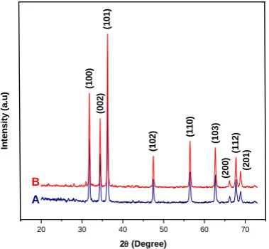
The XRD patterns of the synthesized ZnO samples are shown in Fig. 2. The XRD patterns of the samples reveal that all peaks correspond to the characteristic peaks of the hexagonal wurtzite structure of ZnO with space group P63mc and lattice parameters of a = b =
0.3250 nm and c = 0.5207 nm according to the JCPDS database 36-1451. No peaks of any other phase are detected, indicating that the ZnO samples obtained by current synthetic route are highly pure. The indexed ZnO peaks in the spectrum have high intensity and narrow spectral width, which indicates that the products are of excellent crystallinity.
L O A D
ZnO NPs Quantum dots
adsorbed ZnO electrode
Solar radiation
International Journal of Emerging Technology and Advanced Engineering
Website: www.ijetae.com (ISSN 2250-2459,ISO 9001:2008 Certified Journal, Volume 3, Issue 9, September 2013)
416
20 30 40 50 60 70
A B
(2
0
1
)
(1
1
2
)
(2
0
0
)
(1
0
3
)
(1
1
0
)
(1
0
2
)
(1
0
1
)
(0
0
2
)
(1
0
0
)
In
te
n
s
it
y
(
a
.u
)
2 (Degree)
[image:3.595.62.252.147.322.2]
Fig. 2. X-ray diffractograms of ZnO nanostructures.
B. Functional groups
The FTIR spectrum of the CTAB capped ZnO sample A acquired in the range of 4000-400 cm-1 is shown Fig. 3. The band located at 460-560 cm-1 is correlated to the stretching mode of Zn-O [16]. The band at 3420 cm-1 corresponds to O-H mode of vibration. The stretching mode of vibration of C=O is observed at 1400-1650 cm-1.
4000.0 3600 3200 2800 2400 2000 1800 1600 1400 1200 1000 800 600 450.0 0.0
5 10 15 20 25 30 35 40 45 50 55 60 65 70 75 80 85 90 96.9
cm-1 %T
3902 3737
3428 2925
2854
2342
1675
1591 1555
1522
1384 1327
1207
1035 875
795 749
688 617
566 555 498
Fig. 3. FTIR spectrum of ZnO sample (A).
The absorption peaks at 2852 cm-1 and 2923 cm-1 correspond to the stretching modes of methylene groups, which confirms the presence of CTAB.
The result of the IR spectrum of ZnO nanostructures is generally influenced by particle size and morphology [16].
C. Morphology and size of the ZnO samples
[image:3.595.323.538.452.553.2]The SEM images of the CTAB capped ZnO samples are shown in Fig. 4. The SEM image of sample A apparently exhibits granular ZnO nanostructures. The diameter of the granular ZnO nanostructures are in the range of 30-40 nm. The SEM image of sample B also demonstrates granular ZnO nanostructures with the diameter in the range of 20-30 nm.
Fig. 4. SEM images of ZnO samples.
The TEM images of the CTAB capped ZnO samples are shown in Fig. 5. The average size obtained by TEM image of sample A is 33 nm and that of B is 24 nm. The TEM images clearly show that the average particle size is reduced with increasing capping agent concentration.
Fig. 5. TEM images of ZnO samples.
D. Optical properties of ZnO nanoparticles
[image:3.595.63.265.457.656.2]International Journal of Emerging Technology and Advanced Engineering
Website: www.ijetae.com (ISSN 2250-2459,ISO 9001:2008 Certified Journal, Volume 3, Issue 9, September 2013)
417
200 300 400 500 600 700 800 9000.0 0.1 0.2 0.3 0.4 0.5 0.6 0.7
0.8 B - 361 nm
A - 368 nm
A
b
s
o
rb
a
n
c
e
[image:4.595.73.256.147.318.2]Wavelength (nm)
Fig. 6. UV-vis absorption spectra of ZnO samples
The absorption peak also shifts towards shorter wavelength as the capping agent concentration is increased.
The diffuse reflectance spectra of the ZnO samples are shown in the inset of Fig. 7. The low reflectance values of the samples indicate high absorption in the corresponding wavelength region.
Fig. 7. Plot of (F(R)*hν)^2 vs. hν, Inset: UV-vis diffuse reflectance spectra.
For analysis purposes the diffuse reflectance, R, of the samples can be related to the Kubelka_Munk function F(R) by the relation F(R) = (1-R)2/2R [18]. The band gap energy (Eg) for the ZnO nanostructures is determined by
the plot of the square of the modified Kubelka_Munk function vs. the photon energy (hν), shown in Fig. 6 [19]. The Eg values of the ZnO samples A, B are determined to
be 3.38 eV and 3.39 eV respectively by the extrapolation of the linear portion of the graph down to [F(R)*hν]2 = 0.
The band gap is increased from 3.38 eV to 3.39 nm when the concentration of CTAB is increased. This was explained by the modification of the band structure, i.e; narrowing of the valance band and conduction band [20].
[image:4.595.76.254.443.652.2]International Journal of Emerging Technology and Advanced Engineering
Website: www.ijetae.com (ISSN 2250-2459,ISO 9001:2008 Certified Journal, Volume 3, Issue 9, September 2013)
418
350 400 450 500 550 600
570 nm
570 nm
461 nm
455 nm
398 nm
392 nm
B
A
In
te
n
s
it
y
(
a
.u
)
Wavelength (nm)
Fig, 8. PL spectrum of ZnO samples.
Therefore, the ZnO nanostructures synthesized in the present work would be a promising material for applications in optoelectronic nanodevices in future.
V. CONCLUSION
ZnO nanostructures were prepared by a cost effective and simple sol-gel method using zinc acetate dihydrate, ammonium hydroxide and CTAB. The XRD analysis confirmed that the nanoparticles have the hexagonal
wurtzite-type structure of ZnO. The FTIR spectrum
revealed the functional group assignments of the ZnO nanostructures with CTAB. SEM and TEM images of the samples showed the morphology and size of the ZnO nanostructures. The average particle size is reduced from 33 nm to 24 nm by increasing the concentration of the capping agent. The UV-vis absorption spectra of the the ZnO samples exhibit a blue-shift in cut off wavelength with respect to the bulk. A wider band gap, Eg value is
obtained from ZnO sample B which has smaller particle size. The PL intensity is increased as a function of CTAB concentration, indicating that the defects and the average particle size are decreased when the CTAB concentration is increased. The particle size and excellent optical properties of as-synthesized ZnO nanostructures pave the way for their application in QDSSC.
REFERENCES
[1] Wang, Z. L. (2008). ACS Nano, 2, (1987).
[2] Y.S. Kim, W.P. Tai, S.J. Shu, Thin Solid Films 491 (2005) 153-160.
[3] Sounart, T. L., Liu, J., Voigt, J. A., Hsu, J. W. P., Spoerke, E. D., Tian, Z., & Jiang Y. (2006). Adv.Funct.Mater., 16, 335.
[4] Hsu, J. W. P., Tian, Z. R., Simmons, N. C., Matzke, C. M.,Voigt, J. A., & Liu, J. (2005). Nano Lett., 5, 83.
[5] Stroyuk, O. L., Dzhagan, V. M., Shvalagin, V. V., & Kuchmiy, S. Y. (2010). J. Phys. Chem. C., 114, 220.
[6] Wu, Y., & Yang, P. (2001). J. Am. Chem. Soc., 123, 3165. [7] Park, W. I., Yi, G. C., Kim, M., & Pennycook, S. J. (2002). Adv.
Mater., 24, 1841.
[8] Krunks, M, & Melikov, E. (1995). Thin Solid Films, 270,33. [9] Pan, Z. W, Dai, Z. R., & Wang, Z. L. (2001). Science, 291, 1947. [10] Satoh, Y., Ohshio, S., & Saitoh, H. (2005). Sci. Technol. Adv.
Mater., 6, 215.
[11] Yasuda, T., & Segawa, Y. (2004). Phys. Status Solidi.b., 241, 676. [12] El-Shaer, A., Mofor, A.C., Bakin, A., Kreye, M. & Waag, A.
(2005). J. Superlatt. Microstruct, 38, 265.
[13] Wang, Z. L. (2004). J. Phys. Condens. Matter., 16, R829. [14] Hu Y. and Chen H.J., (2008), J. Nanopart. Res. 10, 401-407. [15] Singh, N., Mehra, R.M., Kapoor, A., Soga, T. J. Renewable
Sustainable Energy, (2011), 4, 013110.
[16] H.M. Ismail, J. Anal. Appl. Pyrolysis 21 (1991) 315. [17] X.M. Hou, F. Zhou, W.M. Liu, Mater. Lett. 60 (2006) 3786. [18] Kortum, G. Reflectance Spectroscopy; Springer – Verlog: New
York (1969).
[19] Cao, G., Rabenberg, L. K., Nunn, C. M, Mallouk, T.E. Chem. Matter. 3, 149-156 (1991).
[20] M. Chakrabarti, S. Dutta, S. Chattapadhyay, A. Sarkar, D. Sanyal and A. Chakrabarti, Nanotechnology. 15[12] (2004) 1792-1796. [21] X. L. Wu, G. G. Siu, C. L. Fu, and H. C. Ong, Appl. Phys. Lett.
78, 2285 (2001).
[22] Li, Y., Feng, H., Zhang, N., & Liu, C. (2009). Mater. Sci. Poland, 27, 551.
[23] Jianguo Zhou, Fengying Zhao, Yingling Wang, Yan Zhang, Lin Yang, (2007), J. Luminenescence 122 pp. 195-197.
[24] Dai.Y, Zhang.Y, Bai.Y, Wang.Z.L, J. Chemical Physics Letters, (2003), 375 (1/2): 96-101.