© 2017, IRJET | Impact Factor value: 5.181 | ISO 9001:2008 Certified Journal | Page 636
Design and Analysis of High Gain Differential Amplifier Using Various
Topologies
SAMARLA.SHILPA
1, J SRILATHA
21
Assistant Professor, Dept of Electronics and Communication Engineering, NNRG, Ghatkesar, Hyderabad, India.
2Dept of Electronics and Instrumentation Engineering, CVRCE, Ibrahimpatnam, Hyderabad, India.
---***---Abstract -
The objective of this paper is to design a differential amplifier using different topologies. Differential amplifiers are the basic building block in the analog circuit design. The characteristics of the differential amplifier are measured by Gain, Common mode Rejection Ratio, and Gain-Bandwidth product. In this paper a high performance differential amplifiers are designed using different approaches and a comparison is made between them. A low pass filter is designed using a differential amplifier. This work presents the optimized architecture of a differential amplifier. The simulation results are verified by using virtuoso 6.1, 0.18um technology at supply voltage 1.8v. The design is implemented using cadenceEDA environment and simulated using Analog design environment.Key Words: Differential Amplifier, Low Voltage and High Gain, CMRR.
1. INTRODUCTION
Over the past few years, the electronics industry has made tremendous changes in the in the era of VLSI technology. The major changes came through in the market are due to the invention of MOS transistors. Integration of IC’s from small scale, medium scale, large scale to over ultra large scale integration has lead many changes in the electronic industry.
It consists of mainly memory, small or micro and logic sales, has contributed a worldwide sales of approximately 75% with the MOS transistors, which enhances the strength of CMOS technology. CMOS technology involves in mainly satisfying all the design constraints like power, area, and speed by minimizing the feature size and using the optimization techniques by lowering the supply voltage, using VTCMOS and MTCMOS etc.
CMOS technology has more advantage than an NMOS technology design due to the design flexibility and easily configurable. Hence CMOS has got a rapid acceptance in the upcoming technology in the area of analog, digital and mixed integrated circuits, like RF communication field, signal processing and biomedical applications etc.
1.1
Differential Amplifier
The differential amplifier is the most important block in designing any analog circuit. The differential amplifiers are designed using bipolar transistors and MOS transistors. An amplifier is a circuit that amplifies any weak signal and strengthens it which is used mainly in communication to transmit a signal over long distance and the signal may be analog or digital.
A differential amplifier circuit amplifies the difference of any two input signals and rejects any two common signals. The ideal characteristics of an amplifier are infinite gain, infinite bandwidth and infinite common mode rejection ratio, high input impedance and low output admittance, less distortion, sensitivity. Also it has less harmonic distortion and increased output voltage swing and the performance of the circuit is measured by its characteristics.
Differential amplifiers are widely used due to less distortion in the output and are widely used in linear amplification circuits. A differential amplifier can be designed in many ways where the output may be single ended or double ended. The most commonly used amplifier is double ended means which has two inputs and which gives two outputs and is commonly known as fully differential amplifier. The advantages of fully differential amplifier over single ended are simple biasing, high immunity to noise, and high linearity. But the disadvantage is large area.
The fully differential amplifier amplifies the difference of two input signals which are out of phase and rejects the signals which have common phase due to any noise induced. This is measured or termed as common mode rejection ratio (CMRR) and its offset voltage. An ideal amplifier circuit has infinite CMRR.
© 2017, IRJET | Impact Factor value: 5.181 | ISO 9001:2008 Certified Journal | Page 637
1.1.1
Differential Amplifier with Passive Load:
Different types of differential amplifiers are studied, designed and analyzed in terms of its performance. A comparison is made to analyze the circuit by varying the design parameters.
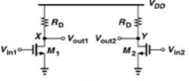
Fig 1.Basic differential amplifier with passive load. The basic differential amplifier is shown in fig 1, it i s designed by using two n-channel MOSFETs M1 and M2 to form a differential pair. The resistors RD are used as load to drive the transistors into saturation. The two input voltages Vin1 and Vin2 are applied at the gate terminal of the MOS transistors, which are equal in magnitude and opposite in phase. The output voltage is measured across two nodes X and Y. The differential signal is measured between these nodes which have equal magnitude and opposite phase to the inputs. The major advantage of this circuit is it has greater output voltage swing.
When two inputs Vin1 and Vin2 are applied with same magnitude and same phase i.e Vin,CM does the effect on the trans conductance of the MOS transistors and which in turn effects the bias current and leads to change the output voltage gain and also further decreases the output voltage swing. If suppose the value of Vin,CM is low then it may turn off M1 and M2, hence no amplification but the output will be clipped off. Hence a minimum bias current is required to maintain the common mode level.
1.1.2 Differential Amplifier with Passive Load and
Ideal Current Source:
The problem of biasing is overcome by using a constant current source Iss in the circuit. The circuit shown in fig 2 uses a constant current source which is used to maintain a minimum bias current and also to avoid the effects of the common mode level changes in the output.
In this circuit the ideal current source is replaced by a transistor driven a constant voltage source and operated in saturation region and hence it acts as a constant current source.
Fig2: Differential Amplifier with Current Source. When Vin1=Vin2 then Vin,CM will be zero, then both M1 and M2 will be in OFF. To study the characteristics and the behavior of the circuit change Vin,CM from 0 to VDD.
1.1.3
Differential Amplifier with Active Load:
Here the circuit is designed by using different load using active components and they can be like diode-connected or current source loads. The diode connected load has an advantage of overcoming the problem of lowering the voltage swing and effect on gain due to common mode.
In this circuit we use PMOS transistors as load by selecting proper dimensions and proper bias current. To achieve high gain, the aspect ratio W/L of PMOS must decrease, and VGS -VTH of PMOS must be increased to compensate the common mode level at X and Y nodes.
Fig3: Differential amplifier with active load
In this circuit we replace the resistors by active devices (NMOS) M3 and M4 and driven by external source to be in saturation. The external bias affects the trans conductance of M1 and M2, so to avoid this effect the tail current by Iss is set properly. If Vin1=Vin2=Vin,CM then ID1=ID2=0 so, both M1 and M2 are OFF and at the same time M3 will be in triode region, hence there will be no amplification and leads to Vout1=Vout2=VDD.
If Vin,CM is increased positively then M1 and M2 will be ON
[image:2.595.62.258.185.269.2]© 2017, IRJET | Impact Factor value: 5.181 | ISO 9001:2008 Certified Journal | Page 638 a constant current through M1 and M2. We conclude that for
proper operation, Vin, CM ≥ VGS1 + (VGS3 – VTH3).
If Vin,CM is further increased then output voltages will remain
constant but at some point M1 and M2 enters into triode region when Vin, CM > Vout1 + VTH = VDD – RDIss/2+VTH.
1.1.4
Differential Amplifier with Active Load
(Current mirror):
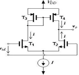
Fig 4: Differential Amplifier with Active Current Mirror Configuration.
In this circuit the external biasing is removed and a differential pair with current mirror is configured as active load. The main purpose of this configuration is it converts a fully differential input to single-ended output. Here the transistors T3 and T4 are similar to each other. The transistor T3 is used to enhance the gain, for example if VGS at T1 is increased by a little amount, the ID1 increases by ∆ID1 and ID2 decreases by ∆ID2.
Similarly ID3 and ID4 and also increases by ∆I, thereby increasing the output voltage and leads to high gain. This is done due to the reduced drain current of T2 and increased drain current of T4. The T4 and T2 are paired such that T4 helps T2 for a change in output voltage.
1.2 Simulation Results:
The frequency response of the basic differential amplifier and other circuits are presented. The magnitude and phase response are shown, and single side output voltage gain is measured.
The design was implemented using cadence EDA tool, 180nm technology. A detailed analysis like DC, transient and AC analysis are done and a comparison is made for all the circuits.
Fig 5: Basic Differential amplifier Circuit with passive load.
Fig 6: Transient Response of the basic Differential Amplifier.
[image:3.595.308.543.100.253.2] [image:3.595.94.233.213.344.2] [image:3.595.310.522.283.452.2] [image:3.595.309.525.486.605.2]© 2017, IRJET | Impact Factor value: 5.181 | ISO 9001:2008 Certified Journal | Page 639 Fig 8: Differential Amplifier with Current Source.
[image:4.595.85.560.49.266.2]Fig 9: AC response of the Differential Amplifier with Current Source.
[image:4.595.81.557.305.487.2]Fig 10: Differential Amplifier with Active (MOS) Load.
Fig 11: AC response of the Differential Amplifier with MOS Load.
Fig 12: Differential Amplifier with Diode Connected topology.
[image:4.595.37.261.532.742.2] [image:4.595.306.565.537.733.2]© 2017, IRJET | Impact Factor value: 5.181 | ISO 9001:2008 Certified Journal | Page 640 Table 1 show the results which are obtained by simulating
the circuits using virtuoso 6.1.
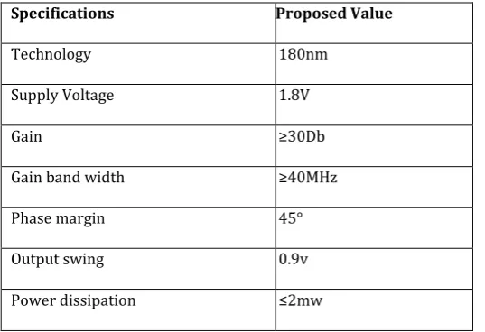
Table-1: Design specifications
Specifications Proposed Value
Technology 180nm
Supply Voltage 1.8V
Gain ≥30Db
Gain band width ≥40MHz
Phase margin 45°
Output swing 0.9v
Power dissipation ≤2mw
The comparison between all the different topologies is given below.
Topology
Voltage Gain
(dB)
3dB Bandwidth
(GHz)
Power Dissipation
(mW)
Differential
Amplifier with
Passive Load
16.01 7.67 6.04
Differential Amplifier with ideal Current Source
14.22 7.99 5.72
Differential
Amplifier with
Active Load
21.19 7.5 2.13
Differential
Amplifier with
Diode Connected topology
35.43 7.98 1.83
1.3 CONCUSION:
In this paper, the different topologies of differential amplifiers have been designed and analyzed in terms of gain, gain bandwidth product, and CMRR. The designs are operated at 1.8 V using 0.18µm technologies.
REFERENCES
[1] Zhang, N. and Hungchi Lee, 2004. Design of a Fully Differential Transconductance Amplifier for A/D Converters. EE240 Term Project Report.
[2] Crawlev, P.J. and G.W. Roberts, 1999. Designing Operational Transconductance Amplifier For Low Voltage Operation. Montreal, Pq, Canada H3A 2A7. [3] E.Sackinger andW.Guggenbuhl, “Design of Fully
Differential CMOS Amplifier for Clipping Control Circuit” World Applied Science Journal 3(1), pp. 110-113, 2008.
[4] A.D. Grasso and S. Pennisi, “High-Performance CMOS Pseudo-Differential Amplifier”, Circuits and Systems, ISCAS 2005. IEEE International Symposium on, pp. 1569 – 1572, 23-26 May 2005.
[5] Zihong Liu, Chao Bian and Zhihua Wang “Full Custom Design of a Two- Stage Fully Differential CMOS Amplifier with High Unity-Gain Bandwidth and Large Dynamic Range at Output”, 48th IEEE International Midwest Symposium on Circuits and Systems, Cincinnati, Ohio, U.S.A., 7-10 August,2005.
BIOGRAPHIES
S.SHILPA, is an Assistant Professor in the department of Electronics and Communication Engineering in NNRG college. She acquired her Master of engineering degree in VLSI System Design in 2012, Her area of research interest includes Low power VLSI Design,
[image:5.595.29.280.394.636.2]